EP1229583A1 - Semiconductor device and its manufacturing method - Google Patents
Semiconductor device and its manufacturing method Download PDFInfo
- Publication number
- EP1229583A1 EP1229583A1 EP01948030A EP01948030A EP1229583A1 EP 1229583 A1 EP1229583 A1 EP 1229583A1 EP 01948030 A EP01948030 A EP 01948030A EP 01948030 A EP01948030 A EP 01948030A EP 1229583 A1 EP1229583 A1 EP 1229583A1
- Authority
- EP
- European Patent Office
- Prior art keywords
- semiconductor
- metal
- electrode terminal
- semiconductor chip
- wiring
- Prior art date
- Legal status (The legal status is an assumption and is not a legal conclusion. Google has not performed a legal analysis and makes no representation as to the accuracy of the status listed.)
- Withdrawn
Links
Images



Classifications
-
- H—ELECTRICITY
- H10—SEMICONDUCTOR DEVICES; ELECTRIC SOLID-STATE DEVICES NOT OTHERWISE PROVIDED FOR
- H10W—GENERIC PACKAGES, INTERCONNECTIONS, CONNECTORS OR OTHER CONSTRUCTIONAL DETAILS OF DEVICES COVERED BY CLASS H10
- H10W74/00—Encapsulations, e.g. protective coatings
- H10W74/01—Manufacture or treatment
- H10W74/012—Manufacture or treatment of encapsulations on active surfaces of flip-chip devices, e.g. forming underfills
-
- H—ELECTRICITY
- H10—SEMICONDUCTOR DEVICES; ELECTRIC SOLID-STATE DEVICES NOT OTHERWISE PROVIDED FOR
- H10W—GENERIC PACKAGES, INTERCONNECTIONS, CONNECTORS OR OTHER CONSTRUCTIONAL DETAILS OF DEVICES COVERED BY CLASS H10
- H10W72/00—Interconnections or connectors in packages
- H10W72/071—Connecting or disconnecting
-
- H—ELECTRICITY
- H10—SEMICONDUCTOR DEVICES; ELECTRIC SOLID-STATE DEVICES NOT OTHERWISE PROVIDED FOR
- H10W—GENERIC PACKAGES, INTERCONNECTIONS, CONNECTORS OR OTHER CONSTRUCTIONAL DETAILS OF DEVICES COVERED BY CLASS H10
- H10W20/00—Interconnections in chips, wafers or substrates
- H10W20/40—Interconnections external to wafers or substrates, e.g. back-end-of-line [BEOL] metallisations or vias connecting to gate electrodes
-
- H—ELECTRICITY
- H10—SEMICONDUCTOR DEVICES; ELECTRIC SOLID-STATE DEVICES NOT OTHERWISE PROVIDED FOR
- H10W—GENERIC PACKAGES, INTERCONNECTIONS, CONNECTORS OR OTHER CONSTRUCTIONAL DETAILS OF DEVICES COVERED BY CLASS H10
- H10W72/00—Interconnections or connectors in packages
- H10W72/90—Bond pads, in general
-
- H—ELECTRICITY
- H10—SEMICONDUCTOR DEVICES; ELECTRIC SOLID-STATE DEVICES NOT OTHERWISE PROVIDED FOR
- H10W—GENERIC PACKAGES, INTERCONNECTIONS, CONNECTORS OR OTHER CONSTRUCTIONAL DETAILS OF DEVICES COVERED BY CLASS H10
- H10W74/00—Encapsulations, e.g. protective coatings
- H10W74/10—Encapsulations, e.g. protective coatings characterised by their shape or disposition
- H10W74/15—Encapsulations, e.g. protective coatings characterised by their shape or disposition on active surfaces of flip-chip devices, e.g. underfills
-
- H—ELECTRICITY
- H10—SEMICONDUCTOR DEVICES; ELECTRIC SOLID-STATE DEVICES NOT OTHERWISE PROVIDED FOR
- H10W—GENERIC PACKAGES, INTERCONNECTIONS, CONNECTORS OR OTHER CONSTRUCTIONAL DETAILS OF DEVICES COVERED BY CLASS H10
- H10W90/00—Package configurations
-
- H—ELECTRICITY
- H10—SEMICONDUCTOR DEVICES; ELECTRIC SOLID-STATE DEVICES NOT OTHERWISE PROVIDED FOR
- H10F—INORGANIC SEMICONDUCTOR DEVICES SENSITIVE TO INFRARED RADIATION, LIGHT, ELECTROMAGNETIC RADIATION OF SHORTER WAVELENGTH OR CORPUSCULAR RADIATION
- H10F39/00—Integrated devices, or assemblies of multiple devices, comprising at least one element covered by group H10F30/00, e.g. radiation detectors comprising photodiode arrays
- H10F39/80—Constructional details of image sensors
- H10F39/809—Constructional details of image sensors of hybrid image sensors
-
- H—ELECTRICITY
- H10—SEMICONDUCTOR DEVICES; ELECTRIC SOLID-STATE DEVICES NOT OTHERWISE PROVIDED FOR
- H10W—GENERIC PACKAGES, INTERCONNECTIONS, CONNECTORS OR OTHER CONSTRUCTIONAL DETAILS OF DEVICES COVERED BY CLASS H10
- H10W20/00—Interconnections in chips, wafers or substrates
- H10W20/40—Interconnections external to wafers or substrates, e.g. back-end-of-line [BEOL] metallisations or vias connecting to gate electrodes
- H10W20/41—Interconnections external to wafers or substrates, e.g. back-end-of-line [BEOL] metallisations or vias connecting to gate electrodes characterised by their conductive parts
- H10W20/425—Barrier, adhesion or liner layers
-
- H—ELECTRICITY
- H10—SEMICONDUCTOR DEVICES; ELECTRIC SOLID-STATE DEVICES NOT OTHERWISE PROVIDED FOR
- H10W—GENERIC PACKAGES, INTERCONNECTIONS, CONNECTORS OR OTHER CONSTRUCTIONAL DETAILS OF DEVICES COVERED BY CLASS H10
- H10W70/00—Package substrates; Interposers; Redistribution layers [RDL]
- H10W70/60—Insulating or insulated package substrates; Interposers; Redistribution layers
-
- H—ELECTRICITY
- H10—SEMICONDUCTOR DEVICES; ELECTRIC SOLID-STATE DEVICES NOT OTHERWISE PROVIDED FOR
- H10W—GENERIC PACKAGES, INTERCONNECTIONS, CONNECTORS OR OTHER CONSTRUCTIONAL DETAILS OF DEVICES COVERED BY CLASS H10
- H10W72/00—Interconnections or connectors in packages
- H10W72/01—Manufacture or treatment
- H10W72/012—Manufacture or treatment of bump connectors, dummy bumps or thermal bumps
- H10W72/01251—Changing the shapes of bumps
- H10W72/01255—Changing the shapes of bumps by using masks
-
- H—ELECTRICITY
- H10—SEMICONDUCTOR DEVICES; ELECTRIC SOLID-STATE DEVICES NOT OTHERWISE PROVIDED FOR
- H10W—GENERIC PACKAGES, INTERCONNECTIONS, CONNECTORS OR OTHER CONSTRUCTIONAL DETAILS OF DEVICES COVERED BY CLASS H10
- H10W72/00—Interconnections or connectors in packages
- H10W72/071—Connecting or disconnecting
- H10W72/072—Connecting or disconnecting of bump connectors
-
- H—ELECTRICITY
- H10—SEMICONDUCTOR DEVICES; ELECTRIC SOLID-STATE DEVICES NOT OTHERWISE PROVIDED FOR
- H10W—GENERIC PACKAGES, INTERCONNECTIONS, CONNECTORS OR OTHER CONSTRUCTIONAL DETAILS OF DEVICES COVERED BY CLASS H10
- H10W72/00—Interconnections or connectors in packages
- H10W72/071—Connecting or disconnecting
- H10W72/072—Connecting or disconnecting of bump connectors
- H10W72/07221—Aligning
-
- H—ELECTRICITY
- H10—SEMICONDUCTOR DEVICES; ELECTRIC SOLID-STATE DEVICES NOT OTHERWISE PROVIDED FOR
- H10W—GENERIC PACKAGES, INTERCONNECTIONS, CONNECTORS OR OTHER CONSTRUCTIONAL DETAILS OF DEVICES COVERED BY CLASS H10
- H10W72/00—Interconnections or connectors in packages
- H10W72/071—Connecting or disconnecting
- H10W72/072—Connecting or disconnecting of bump connectors
- H10W72/07231—Techniques
- H10W72/07234—Using a reflow oven
-
- H—ELECTRICITY
- H10—SEMICONDUCTOR DEVICES; ELECTRIC SOLID-STATE DEVICES NOT OTHERWISE PROVIDED FOR
- H10W—GENERIC PACKAGES, INTERCONNECTIONS, CONNECTORS OR OTHER CONSTRUCTIONAL DETAILS OF DEVICES COVERED BY CLASS H10
- H10W72/00—Interconnections or connectors in packages
- H10W72/071—Connecting or disconnecting
- H10W72/072—Connecting or disconnecting of bump connectors
- H10W72/07231—Techniques
- H10W72/07236—Soldering or alloying
-
- H—ELECTRICITY
- H10—SEMICONDUCTOR DEVICES; ELECTRIC SOLID-STATE DEVICES NOT OTHERWISE PROVIDED FOR
- H10W—GENERIC PACKAGES, INTERCONNECTIONS, CONNECTORS OR OTHER CONSTRUCTIONAL DETAILS OF DEVICES COVERED BY CLASS H10
- H10W72/00—Interconnections or connectors in packages
- H10W72/20—Bump connectors, e.g. solder bumps or copper pillars; Dummy bumps; Thermal bumps
- H10W72/221—Structures or relative sizes
- H10W72/222—Multilayered bumps, e.g. a coating on top and side surfaces of a bump core
-
- H—ELECTRICITY
- H10—SEMICONDUCTOR DEVICES; ELECTRIC SOLID-STATE DEVICES NOT OTHERWISE PROVIDED FOR
- H10W—GENERIC PACKAGES, INTERCONNECTIONS, CONNECTORS OR OTHER CONSTRUCTIONAL DETAILS OF DEVICES COVERED BY CLASS H10
- H10W72/00—Interconnections or connectors in packages
- H10W72/20—Bump connectors, e.g. solder bumps or copper pillars; Dummy bumps; Thermal bumps
- H10W72/241—Dispositions, e.g. layouts
-
- H—ELECTRICITY
- H10—SEMICONDUCTOR DEVICES; ELECTRIC SOLID-STATE DEVICES NOT OTHERWISE PROVIDED FOR
- H10W—GENERIC PACKAGES, INTERCONNECTIONS, CONNECTORS OR OTHER CONSTRUCTIONAL DETAILS OF DEVICES COVERED BY CLASS H10
- H10W72/00—Interconnections or connectors in packages
- H10W72/20—Bump connectors, e.g. solder bumps or copper pillars; Dummy bumps; Thermal bumps
- H10W72/251—Materials
- H10W72/252—Materials comprising solid metals or solid metalloids, e.g. PbSn, Ag or Cu
-
- H—ELECTRICITY
- H10—SEMICONDUCTOR DEVICES; ELECTRIC SOLID-STATE DEVICES NOT OTHERWISE PROVIDED FOR
- H10W—GENERIC PACKAGES, INTERCONNECTIONS, CONNECTORS OR OTHER CONSTRUCTIONAL DETAILS OF DEVICES COVERED BY CLASS H10
- H10W72/00—Interconnections or connectors in packages
- H10W72/20—Bump connectors, e.g. solder bumps or copper pillars; Dummy bumps; Thermal bumps
- H10W72/29—Bond pads specially adapted therefor
-
- H—ELECTRICITY
- H10—SEMICONDUCTOR DEVICES; ELECTRIC SOLID-STATE DEVICES NOT OTHERWISE PROVIDED FOR
- H10W—GENERIC PACKAGES, INTERCONNECTIONS, CONNECTORS OR OTHER CONSTRUCTIONAL DETAILS OF DEVICES COVERED BY CLASS H10
- H10W72/00—Interconnections or connectors in packages
- H10W72/50—Bond wires
- H10W72/551—Materials of bond wires
- H10W72/552—Materials of bond wires comprising metals or metalloids, e.g. silver
- H10W72/5522—Materials of bond wires comprising metals or metalloids, e.g. silver comprising gold [Au]
-
- H—ELECTRICITY
- H10—SEMICONDUCTOR DEVICES; ELECTRIC SOLID-STATE DEVICES NOT OTHERWISE PROVIDED FOR
- H10W—GENERIC PACKAGES, INTERCONNECTIONS, CONNECTORS OR OTHER CONSTRUCTIONAL DETAILS OF DEVICES COVERED BY CLASS H10
- H10W72/00—Interconnections or connectors in packages
- H10W72/851—Dispositions of multiple connectors or interconnections
- H10W72/853—On the same surface
- H10W72/856—Bump connectors and die-attach connectors
-
- H—ELECTRICITY
- H10—SEMICONDUCTOR DEVICES; ELECTRIC SOLID-STATE DEVICES NOT OTHERWISE PROVIDED FOR
- H10W—GENERIC PACKAGES, INTERCONNECTIONS, CONNECTORS OR OTHER CONSTRUCTIONAL DETAILS OF DEVICES COVERED BY CLASS H10
- H10W72/00—Interconnections or connectors in packages
- H10W72/851—Dispositions of multiple connectors or interconnections
- H10W72/874—On different surfaces
- H10W72/884—Die-attach connectors and bond wires
-
- H—ELECTRICITY
- H10—SEMICONDUCTOR DEVICES; ELECTRIC SOLID-STATE DEVICES NOT OTHERWISE PROVIDED FOR
- H10W—GENERIC PACKAGES, INTERCONNECTIONS, CONNECTORS OR OTHER CONSTRUCTIONAL DETAILS OF DEVICES COVERED BY CLASS H10
- H10W74/00—Encapsulations, e.g. protective coatings
-
- H—ELECTRICITY
- H10—SEMICONDUCTOR DEVICES; ELECTRIC SOLID-STATE DEVICES NOT OTHERWISE PROVIDED FOR
- H10W—GENERIC PACKAGES, INTERCONNECTIONS, CONNECTORS OR OTHER CONSTRUCTIONAL DETAILS OF DEVICES COVERED BY CLASS H10
- H10W74/00—Encapsulations, e.g. protective coatings
- H10W74/10—Encapsulations, e.g. protective coatings characterised by their shape or disposition
- H10W74/111—Encapsulations, e.g. protective coatings characterised by their shape or disposition the semiconductor body being completely enclosed
-
- H—ELECTRICITY
- H10—SEMICONDUCTOR DEVICES; ELECTRIC SOLID-STATE DEVICES NOT OTHERWISE PROVIDED FOR
- H10W—GENERIC PACKAGES, INTERCONNECTIONS, CONNECTORS OR OTHER CONSTRUCTIONAL DETAILS OF DEVICES COVERED BY CLASS H10
- H10W90/00—Package configurations
- H10W90/701—Package configurations characterised by the relative positions of pads or connectors relative to package parts
- H10W90/721—Package configurations characterised by the relative positions of pads or connectors relative to package parts of bump connectors
- H10W90/722—Package configurations characterised by the relative positions of pads or connectors relative to package parts of bump connectors between stacked chips
-
- H—ELECTRICITY
- H10—SEMICONDUCTOR DEVICES; ELECTRIC SOLID-STATE DEVICES NOT OTHERWISE PROVIDED FOR
- H10W—GENERIC PACKAGES, INTERCONNECTIONS, CONNECTORS OR OTHER CONSTRUCTIONAL DETAILS OF DEVICES COVERED BY CLASS H10
- H10W90/00—Package configurations
- H10W90/701—Package configurations characterised by the relative positions of pads or connectors relative to package parts
- H10W90/731—Package configurations characterised by the relative positions of pads or connectors relative to package parts of die-attach connectors
- H10W90/732—Package configurations characterised by the relative positions of pads or connectors relative to package parts of die-attach connectors between stacked chips
-
- H—ELECTRICITY
- H10—SEMICONDUCTOR DEVICES; ELECTRIC SOLID-STATE DEVICES NOT OTHERWISE PROVIDED FOR
- H10W—GENERIC PACKAGES, INTERCONNECTIONS, CONNECTORS OR OTHER CONSTRUCTIONAL DETAILS OF DEVICES COVERED BY CLASS H10
- H10W90/00—Package configurations
- H10W90/701—Package configurations characterised by the relative positions of pads or connectors relative to package parts
- H10W90/751—Package configurations characterised by the relative positions of pads or connectors relative to package parts of bond wires
- H10W90/756—Package configurations characterised by the relative positions of pads or connectors relative to package parts of bond wires between a chip and a stacked lead frame, conducting package substrate or heat sink
-
- H—ELECTRICITY
- H10—SEMICONDUCTOR DEVICES; ELECTRIC SOLID-STATE DEVICES NOT OTHERWISE PROVIDED FOR
- H10W—GENERIC PACKAGES, INTERCONNECTIONS, CONNECTORS OR OTHER CONSTRUCTIONAL DETAILS OF DEVICES COVERED BY CLASS H10
- H10W90/00—Package configurations
- H10W90/811—Multiple chips on leadframes
Definitions
- the invention relates to a so-called chip-on-chip (hereinafter abbreviated as COC) type semiconductor device, in which a plurality of semiconductor chips is electrically interconnected as opposed to each other, and a method for manufacturing the same. More particularly, the invention relates to a semiconductor device having such a construction that two mutually opposed semiconductor chips thereof can be joined to each other without being damaged due to a high temperature applied thereon or mechanical shock by supersonic waves when they are connected to each other and a method for manufacturing the same.
- COC chip-on-chip
- COC chip on chip
- a COC (chip on chip) type semiconductor device having a construction of composing a semiconductor circuit of a plurality of chips by interconnecting them one on the other for a purpose of, for example, reducing an occupied area by means of three-dimensioning or standardizing part of the circuit (for example, changing driver circuits based on application by standardizing the memory portions), if the semiconductor device is composed of a plurality of circuits like in the case of a combination of memory portions and the corresponding driver circuits.
- a semiconductor device having the above-mentioned construction is fabricated by fixing the one semiconductor chip 1 on a heated board stage 51 and the other semiconductor chip 2 to a mount head 52, pressing the mount head 52 to permit bump electrodes 11 and 21 made of Au etc. of the respective chips to come in contact with each other under pressure, and heating it to a temperature of 450°C or so to interconnect these bump electrodes 11 and 21 electrically.
- the bumps 11 and 21 are made of a metal material such as Au having a higher melting point than solder because the semiconductor device is mounted on the mother board by soldering.
- the above-mentioned COC type semiconductor device employs high melting point metal such as Au as the material of its bump electrodes, to interconnect a plurality of semiconductor chips thereof, it is necessary to heat them to a temperature of 450°C or so under pressure in order to obtain good electrical interconnection.
- the semiconductor substrate is also heated to a temperature of 450°C or higher, so that the circuit elements formed in the semiconductor substrate (elements such as transistors constituting the semiconductor device) are heated to a high temperature, thus fluctuating in properties, which is a problem.
- these chips can be joined to each other at a temperature of 450°C or so, if under pressure as mentioned above, for example, once joined to each other, they cannot be separated without being destroyed in most cases because Au has a high melting point.
- a semiconductor device includes; a first semiconductor chip having an electrode terminal, a second semiconductor chip having an electrode terminal, a bump electrode made of a first metal for joining the first and second semiconductor chips, the bump electrode being provided on at least one of the electrode terminal of the first semiconductor chip and the electrode terminal of the second semiconductor chip, and an alloy layer formed on a joining portion where the first and second semiconductor chips are joined with each other via the bump electrode, the alloy layer being made of an alloy of the first metal and a second metal, wherein the second metal is made of such a metal that can melt at a temperature lower than a melting point of the first metal and be alloyed with the first metal.
- the first or second metal referred to here includes not only pure metal but also an alloy and composite metal made of at least two kinds of metal as well as main metal on the outer layer side in a case of a stack containing at least two kinds of metal.
- an alloy layer of the first and second metal includes an entirely alloy layer as well as such a layer that part thereof is an alloy and the other part is made of only the first or second metal or any other compound.
- the constructions of joining via the bump electrode include a construction in which one bump electrode and another are joined to each other or another in which a bump electrode is provided to the electrode terminal of one semiconductor chip so that it may be directly joined to the electrode terminal of the other semiconductor chip therethrough.
- the bump electrode can be connected at a low heating temperature almost equal to the melting point of the second metal, so that by selecting, for example, Sn as the material of the second metal, it is unnecessary to apply such a heating temperature that may affect the circuit elements, thus avoiding adverse effects on these elements owing to a high temperature.
- the first metal that makes up the major part of the bump electrode has a relatively high melting point and, therefore, causes no trouble at around the soldering temperature during mounting.
- the semiconductor device of the present invention includes; a first semiconductor chip having an electrode terminal, a second semiconductor chip having an electrode terminal, a bump electrode made of a first metal for joining the first and second semiconductor chips, the bump electrode being provided on at least one of the electrode terminal of the first semiconductor chip and the electrode terminal of the second semiconductor chip, and a third metal layer having a lower melting point than that of the first metal provided on a joining portion where the first and second semiconductor chips are joined with each other via the bump electrode.
- the third metal layer having a low melting point such as the alloy formed by the first and second metal
- the third metal layer melts at a relatively low temperature and diffuses into the bump electrode or the electrode terminal to thereby provide diffusive joining.
- the third metal layer also includes not only pure metal but also an alloy etc., so that after being joined, it may be combined or alloyed with the first or second metal to have an uneven composition.
- the third metal layer has a relatively low melting point and melts readily at an elevated temperature, it is very thin and mostly supported by the first metal and, in a package, is not peeled off and, at the same time, may be easily peeled off by an external force when heated.
- the semiconductor device of the present invention includes, a first semiconductor chip having an electrode terminal, a second semiconductor chip having an electrode terminal, a bump electrode made of a first metal for joining the first and second semiconductor chips, the bump electrode being provided on at least one of the electrode terminal of the first semiconductor chip and the electrode terminal of the second semiconductor chip, and a detachable material portion provided on a joining portion where the first and second semiconductor chips are joined with each other via the bump electrode, the detachable material being made of such a material that the first and second semiconductor chips can be easily separated from each other at a temperature of 280°C to 500°C.
- the joining portion is joined to by such metal that melts at a lower temperature, for example, 300°C or lower, so that the metal with a lower melting point provides a very thin layer and can hardly be peeled off at around a temperature of 300°C but be easily peeled off by an external force at around that temperature in construction.
- the bump electrode is formed on the electrode terminal of each of the first and second semiconductor chips
- the bump electrode is formed on the electrode terminal of either one of the first and second semiconductor chip so that a metal film made of the first or second metal may be formed on the electrode terminal of the other semiconductor chip
- the alloy layer is formed on the joining portion between these bump electrodes or between the bump electrode and the electrode terminal respectively.
- at least one of the bump electrodes is made of the first metal, so that it can be alloyed with the second metal provided on the right and side face of the bump electrode to thereby joined to via an alloy layer, or joined to via the third metal layer. And they are joined securely by forming a fillet at the joining portion even with a small size of the bump electrode.
- a fillet made of the alloy layer of the first and second metal or of the third metal may be formed on the joining portion between the first and second semiconductor chips, thus highly securing the joining.
- the fillet here refers to such a portion of the joining portion that protrudes out on the side of the side wall, including a smoothly sloped one as well as a small one protruded only in the vicinity of the joining portion.
- the joining portion comes to have the Au-Sn alloy, thus making it possible to connect a bump electrode only by applying a relatively low temperature of 300°C or so, at which the circuit elements are not affected.
- the semiconductor device of the present invention includes; a first semiconductor chip having an electrode terminal or a wiring, a second semiconductor chip having an electrode terminal or a wiring, and a low-melting point metal layer provided on the surface of the wiring of at least one of the first and second semiconductor chips, wherein the first and second semiconductor chips are electrically interconnected and joined to each other via the low-melting point metal layer so that the electrode terminal or wiring is face to face each other.
- the low-melting point metal layer includes a joining portion which at least partially has an alloy formed thereon due to alloying of the first and second metal or a boundary portion which is joined in a diffusive manner owing to the provision of the third metal.
- the wiring can be formed via a second insulating layer onto a passivation film on the semiconductor chip, thus joining the joining portion in secure contact even if the bump electrode of the joining partner semiconductor chip or even if the wiring portions are directly joined to each other without bump electrodes.
- the first and second semiconductor chips are joined to each other between their respective wirings, and the low-melting point metal layer is provided on a joining portion, and further including a first insulating layer provided as interposed at a gap between the a couple of wirings except at the joining portion, thus securely interconnecting the wiring with no possible contact between the wiring provided on the outermost surface.
- the wiring can be made of an Au via a barrier metal layer provided to the electrode terminal as connected thereto, and the low-melting point metal layer can be made of an Au-Sn alloy. Further the wiring can include a Cu wiring made of Cu formed simultaneously with the electrode terminal, a barrier metal layer provided on the Cu wiring, and an Au wiring provided on the barrier metal layer, wherein the low-melting point metal layer is made of an Au-Sn alloy and is provided on the Au wire. Further the wiring can be made of Au formed simultaneously with the electrode terminal, and the low-melting point metal layer can be made of an Au-Sn alloy.
- the joining portion By forming the Au-Sn alloy constituting the joining portion so that it may be rich in Au by containing Au by 65 weight-percent or more, an eutectic alloy can be obtained, so that the joining portion can be connected securely and still can be easily removed by heating it to a temperature of 300°C or so because the eutectic alloy has a low melting point. Further, the joining strength can be stabilized even more if the Au-Sn alloy layer of the joining portion is 0.8 ⁇ m or more and 5 ⁇ m or less.
- the gap in the joining portion between the first and second semiconductor chips is filled with an insulating resin having nearly the same elastic modulus as the bump electrode, even though a compressing force due to, for example, shrinkage of the resin package is applied on these chips, the pressure on the semiconductor layer is not concentrated to the electrode terminal portion such as the bump electrode but is dispersed all over the surfaces of the semiconductor chips and, therefore, can be absorbed evenly by the surfaces, thus improving the reliability of the device.
- the gap between the first and second semiconductor chips joined each other is filled with an insulating resin layer with a thermal shrinkage factor of 4% or less, even though both semiconductor chips are adhered to each other at a temperature of 300°C or so and then cooled down to the room temperature, they do not shrink than the electrode terminal connecting portion such as the bump electrode, so that the compressing force is not concentrated to the electrode terminal portion but is dispersed all over the surfaces of the semiconductor chips and, therefore, can be absorbed evenly by the surfaces, thus improving the reliability of the device.
- a circuit element is formed in the semiconductor layer at the joining portion of at least one of the first and second semiconductor chips, thus improving the integration density. That is, by the present invention, the chips can be joined to each other at a relatively low temperature with almost no pressure applied thereon, thus making it possible to form the circuit element even under the electrode pad or wiring joining portions.
- a method for manufacturing a semiconductor device of the present invention in which a first semiconductor chip or substrate and a second semiconductor chip are joined to each other with the surfaces thereof on which an electrode terminal or a wiring are formed respectively as facing each other via metals of the surface of the electrode terminal or the wiring, comprising the steps of; providing at least one of the metals with a low-melting point metal layer having a lower melting point than that of each of the metals, and melting the low-melting point metal layer or alloying the metals with the low-melting point metal layer to thereby join the first semiconductor chip or substrate and the second semiconductor chip to each other.
- Another method for manufacturing a semiconductor device of the present invention in which a first semiconductor chip or substrate and a second semiconductor chip are joined to each other with the surfaces thereof on which an electrode terminal or a wiring are formed respectively as facing each other via metals of the surface of the electrode terminal or the wiring, comprising the steps of; providing at least one of the metals with a low-melting point metal layer having a lower melting point than that of each of the metals, and liquefying the low-melting point metal layer to thereby diffuse the metals provided on the surface of the electrode terminal or the wiring into the liquefied low-melting point metal, by the liquid-phase diffusion method, thus joining the first semiconductor chip or substrate and the second semiconductor chip to each other.
- the metals are made of Au and the low-melting point metal layer is made of Sn or an Au-Sn alloy and also the first semiconductor chip or substrate and the second semiconductor chip are superposed one on the other with the electrode terminals or the wirings thereof as facing each other and heated to a temperature at which the Au-Sn alloy or Sn melts, to be self-aligned and joined with each other. That is, when these portion can be joined to each other by use of the Au-Sn alloy and heating them to a temperature of 280°C or so, they melt completely and, therefore, needs no pressure application nor complete alignment, to be brought up by surface tension to the joining position such as the bump in self-alignment.
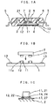
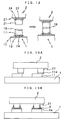
- a semiconductor device according to the present invention has such a COC type construction that onto a semiconductor chip 1 on the surface of which bump electrodes 11 are formed, bump electrodes 21 of a second semiconductor chip 2 are joined.
- the respective bumps electrodes 11 and 21 of these first and second semiconductor chips 1 and 2 are both made of first metal such as Au having a relatively high melting point, while a joining portion between these bump electrodes 11 and 21 is formed of an alloy layer 3 given by alloying the first metal and second metal, which second metal can melt at a temperature lower than the melting point of the first metal and be alloyed with it.
- the respective bump electrodes 11 and 21 are formed by plating etc. to a thickness of 10-30 ⁇ m or so, in addition to which the bump electrode 11 of the first semiconductor chip 1 is provided with Sn (second metal) formed thereon to a thickness of 0.5-3.0 ⁇ m by electroless plating or sputtering.
- the bump electrodes 11 and 21 themselves are formed conventionally in that, as shown in FIG.
- barrier metal layer 14 and 24 in a two-layer or three-layer construction, for example, which consists of a first layer made of Ti or Cr, a second layer made of W, Pt, Ag, Cu, or Ni, and a third layer made of Au etc.
- the bump electrodes 11 and 21 made of Au, Cu, etc. respectively.
- reference numerals 17 and 27 indicate an insulator film.
- An Sn coating 11a is provided on the bump electrode 11 made of Au, so that at around a temperature of 230°C, Sn with a melting point of 232°C or so melts to be alloyed with Au having a melting point of 1064°C to thereby provide an eutectic alloy and, at around a temperature of 280°C, an alloy layer 3 made of an Au-Sn alloy is formed on the joining surface to permit both the bump electrode 11 and 21 to be melt-adhered to each other.
- a memory driver circuit is formed on its semiconductor substrate, on the surface of which are provided an inter-layer insulator film and a wiring layer, on the surface of which are in turn formed the electrode terminal 12 for finally connecting with the second semiconductor chip 2 having memory circuit elements etc. and an electrode terminal 13 for connecting with an external lead.
- On this electrode terminal 12 is formed the bump electrode 11 via a barrier metal layer 14 as mentioned above.
- These circuit elements (semiconductor elements) and the wirings, electrode terminals, insulator films, etc. formed on the surface of the semiconductor substrate are manufactured by almost the same method as that for ordinary semiconductor devices. Note here that besides silicon, which is employed typically, any other compound semiconductor such as GaAs may be employed as the material of the substrate.
- the second semiconductor chip 2 for example, memory circuits are formed in a matrix, in such a configuration that portions connected to the driver circuit or the external lead are formed as the electrode terminal 22 on the surface of its semiconductor substrate, on the surface of which electrode terminal 22 is also formed the bump electrode 21 made of Au like in the case of the first semiconductor chip 1.
- This bump electrode 21 may have, if desired, an Sn coating formed thereon like in the case of the first semiconductor chip 1.
- the first semiconductor chip 1 has no Sn coating formed thereon
- the second semiconductor chip 2 may has an Sn coating formed only on the bump electrode 21. That is, it is only necessary to provide the Sn coating on at least one of these two chips.
- the second semiconductor chip 2 need not be an IC but may be a transistor, a diode, a capacitor, or any other discrete component, which may be not formed on a semiconductor substrate.
- a discrete protective diode is mounted as the second semiconductor chip because it can provide a built-in large-capacitance protective element.
- the first semiconductor chip 1 is put on a substrate stage which can be heated to then superpose the second semiconductor chip 2 thereon by a mounter in rough alignment of the bumps, which is heated to a temperature of 300°C or so while applying thereon load of around its own weight of the second semiconductor chip so that the Sn coating 11a may melt to form an eutectic with Au of the bump electrodes 11 and 21, thus forming the alloy layer 3.
- a mounter in rough alignment of the bumps, which is heated to a temperature of 300°C or so while applying thereon load of around its own weight of the second semiconductor chip so that the Sn coating 11a may melt to form an eutectic with Au of the bump electrodes 11 and 21, thus forming the alloy layer 3.
- the first and second semiconductor chips 1 and 2 are not completely aligned with each other, when the alloy layer 3 is formed at around a temperature of 300°C to melt this alloy layer, the second chip 2 moves, as shown in FIG. 13B, by surface tension of the alloy layer 3 in such a manner that they may be joined center-to-center of bump electrodes 11 and 21 each other (self-alignment). When they are cooled then, the alloy layer 3 is solidified so that they may be adhered to each other.
- This self-alignment is possible not only between one semiconductor chip and another but also between a substrate and a semiconductor chip as well, in which case low-melting point metal such as the Au-Sn alloy layer is melted.
- this example has employed as the load only its own weight of the second semiconductor chip during joining, an extra some weight may preferably be added when the number of the joining portions such as bumps is large to thereby reduce the load for each of them. For example, load of 2 gram for each bump may be applied at a temperature of 350°C in joining.
- the gap between the first and second semiconductor chips 1 and 2 is filled with an insulating resin 7 made of, for example, an epoxy resin or elastomer, so that the semiconductor chips 1 and 2 joined to each other are bonded, like in the case of manufacturing of ordinary semiconductor devices, on a die island 4 made of a lead frame and connected by wire bonding to each lead 5 via a wire 6 made of gold etc. and enclosed by a resin package 8 which is molded. Then, the lead frame has its leads cut off and undergoes forming, to provide a semiconductor device having such a shape as shown in FIG. 1A.
- an insulating resin 7 made of, for example, an epoxy resin or elastomer
- the electrode terminals of the respective first and second semiconductor chips are interconnected and adhered to each other by alloying the first metal of a metal film on the bump electrode or electrode terminal with the coating made of the second metal having a lower melting point than the first metal, so that they can be joined to each other at a relatively low temperature of 300°C or so despite that the bump is made of metal such as Au having a relatively high melting point. Moreover, since they are joined to each other by alloying, the alloy layer will not melt to peel off the joined portions even when it is heated to a temperature of 260°C or so when, for example, the semiconductor device is soldered to a circuit board.
- the semiconductor elements (circuit elements) formed on a semiconductor substrate are not subject to mechanical or thermal stress, so that their properties are not affected at all. This leads to very high reliabilities of the semiconductor device.
- the portion where the second metal coating is provided has some residue thereof, which can, however, be easily peeled off by an external force at an elevated temperature of 300°C or so because the coating has a smaller concentration of the first metal even in the alloyed condition. That is, at a solder reflow temperature, a very thin layer melts, if any, and is not separated because no external force is applied thereon, whereas in the case of, for example, replacement of the semiconductor chips, it can be easily separated by an external force at an elevated temperature of 300°C or so to facilitate the replacement.
- any other alloys may be employed as far as they can be separated at a temperature of 280-500°C because only the joined potion needs to be heated for separation.
- the method of joining by use of a low-melting point metal layer made of Sn etc. according to the present invention is detailed below in comparison to a related art Au-Au joining method.
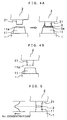
- a related art Au-Au joining method As shown in FIG. 14B, by the related art method of joining one Au bump and another to each other using supersonic waves, an Au bump (solid phase) and another (solid phase) diffuse into each other in solid phase diffusion. As such, the diffusion proceeds very slowly, so that these bumps cannot be joined to each other unless shocked by supersonic waves etc.
- the Au bump is coated with low-melting point metal such as Sn and heated, as shown in FIG.
- Sn melts at a relatively low temperature to be liquefied, so that Au diffuses into the liquid-phase Sn by liquid-phase diffusion. Accordingly, Au diffuses into each other at a relatively low temperature, so that the bumps can be joined to each other at a relatively low temperature without applying supersonic waves thereon.
- This liquid-phase diffusion method is further detailed as follows.
- one of the bumps is coated with low-melting point metal such as Sn to then superpose the first and second semiconductor chips one on the other with their respective joining portions being in contact with each other, which are then heated to a temperature of 350°C with joining load of 2 gram or so applied on each of the bumps.
- Sn is liquefied, so that Au diffuses into the liquid-phase Sn. That is, they enter a liquid-phase diffusion state and, therefore, diffuse into each other by far more rapidly than in diffusion when they are both in a solid phase.
- an Sn-Au alloy layer is formed as shown in the lower part of FIG. 14A. When cooled in this state, these chips are joined to each other completely.
- the second metal coating 11a is illustrated as covering also the side faces of the bump electrode 11.
- a fillet 3a is formed from the surroundings of the small bump electrode 11 up to the larger bump electrode 21 to secure the joining. Also in a case described later with reference to FIG. 4A, by forming such a fillet 3a in joining, the joining can be made strong greatly.
- the fillet 3a here refers to such a portion of a low-melting point metal layer such as the Au-Sn alloy layer that protrudes out from the joining portion to the side walls of the bump electrode etc., which fillet 3a need not always be formed as trailing all over the side walls of one of the two bump electrodes but just needs to be formed to such an extent that the side wall of the bump 21 may be wetted by the low-melting point metal layer partially on the side of the joining portion, in order to improve the joining strength.
- a low-melting point metal layer such as the Au-Sn alloy layer that protrudes out from the joining portion to the side walls of the bump electrode etc.
- the fillet 3a when the fillet 3a is formed as trailing greatly, as shown in FIG. 15, its joining strength was clearly observed to be improved as compared to the case where no fillet is formed.
- the horizontal axis represents the shearing strength (N/mm 2 ) and the vertical axis, the number of articles n (pcs).
- This fillet may be formed not only at the above-mentioned Au-Sn layer but also at the layer where the first metal is alloyed with the second or third metal.
- the Sn coating need not be formed on the side faces of the bump electrode 11 but needs to be formed only on the right surface, that is, the joining surface as shown in FIG. 3. Note here that the same components are indicated by the same reference numerals in FIGS. 3 and 1B. In this case, if the two semiconductor chips once joined to each other may not possibly be dismounted and their bump electrodes have a difference in size, as shown in FIG.
- the fillet 3a is formed to enhance the adhesive strength as shown in the right side of the figure, while by forming the Sn coating 11a on the smaller bump electrode 21, on the other hand, the adhesive strength can be weakened so that the chips can be dismounted easily.
- the Sn coating 11a is formed only one of the bump electrodes 11 and 21, to easily form an alloy layer on the joining surface. That is, since the Au and Sn portions are alloyed with each other in mutual contact for joining, if the Sn coating is provided on both bumps, these two Sn coatings are not readily joined to each other when they came in mutual contact in that first the Au layer and the Sn coating on the respective bump electrodes are alloyed with each other when they came in mutual contact and then Au diffuses into the joining portion to be alloyed with it for joining, so that preferably the Au layer and the Sn coating are formed so that they may be in contact with each other. Alternatively, however, an Sn coating may be formed on both bump electrodes but very thin so that Au can be diffused readily.
- the above-mentioned alloy layer if alloyed in a completely eutectic manner, has a composition of 80 weight-percent of Au and 20 weight-percent of Sn, which however is not heated sufficiently during joining, so that the joining portion hardly provides a complete eutectic alloy. Even if it does not provide a complete eutectic alloy, however, the joining portion can have a secure joining strength as far as it has at least 64 weight-percent of Au and can be separated alone when heated to a temperature of 300°C or so. Also, preferably no alloy layer is formed but an Au layer alone, to enhance the mechanical strength.
- the Sn coating thickness and the joining time and temperature are adjusted so that the Au concentration is at least 65 weight-percent even at the point where the Sn concentration hits the peak and 100 weight-percent at the root of the bump electrodes 11 and 21.
- the Au concentration is meant to be, for example, at least 65 weight-percent not all over the bump electrode surfaces but just over at least 60% of the whole area because the electrodes are not in a complete steady state.
- the joining time and temperature and the Sn layer thickness can be adjusted so that, for example, the Au concentration is at least 65 weight-percent at such a joining portion, still leaving a point where the Au concentration is 100 weight-percent.
- the Au-Sn eutectic layer (joining portion 3) is at least 0.8 ⁇ m and 5 ⁇ or less in thickness.
- the Sn coating must be 0.1 to 4.0 ⁇ m in thickness.
- the Au layer (bump electrode) must be formed thick.
- FIGS. 1A to 1C has the bump electrodes 11 and 21 formed on the electrode terminals of the first and second semiconductor chips 1 and 2 respectively, the bump electrode only needs to be formed on at least one of these electrode terminals as far as it is positioned at the interconnection or may be joined to the electrode terminal.
- FIG. 6 shows an expanded cross-sectional view of only the interconnection. That is, on the connection electrode terminal 12 of the first semiconductor chip 1, instead of a bump electrode, a metal film (Au film) 15 made of, for example, Au with a thickness of 0.2 to 0.5 ⁇ m is provided via the barrier metal layer 14, on which a second metal coating (Sn coating) 16 is provided to the same thickness as the Au film 15.
- the bump electrode 21 made of Au is formed in almost the same manner as above, in such a construction that the bump electrode 21 is alloyed with the Sn coating 16 to thereby be melt-adhered to the Au film 15 overlying the electrode terminal 12.
- This Sn coating 16 may be provided on the side of the bump electrode 21 of the second semiconductor chip 2 or on both sides and connected with them in the same way as the above.
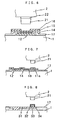
- the first and second semiconductor chips are interconnected between their respective electrode terminals, according to this embodiment of the present invention, by providing the surface of the first metal with a coating of the second metal that can be alloyed with the first metal at a relatively low temperature and heating them, they can be alloyed with each other for joining, so that these chips can directly be joined to each other through the exposed portion of wiring. That is, as shown in FIG. 7, when a wiring 18 made of Au is formed as connected to the electrode terminal 12 made of Al etc.
- the Sn coating 11a can be formed at the joining portion on the Au wiring 18 and abutted against the bump electrode 21 of the second semiconductor chip 2 in contact therewith to be then heated to a temperature of 300°C or so for joining.
- the barrier metal layer 14 serves to prevent the Al electrode terminal 12 from being oxidized so that it may be connected with the Au wiring 18 at a low resistance.
- FIGS. 6 and 7 the same components are indicated by the same reference numerals and, therefore, their explanation is omitted.
- an Al or Cu wiring may be formed in some cases.
- the joining portion of, for example, an Al wiring can be provided with the barrier metal layer, the Au layer, and the Sn coating as shown in FIG. 7 to thereby join the chips easily.
- a Cu wiring on the other hand, as shown in FIG. 8, on a Cu wiring 31, only the joining portion can be provided with a barrier metal layer 32 made of Ti/W or Ni by plating and, thereon, with an Sn coating 34 to thereby be joined with the second semiconductor chip 2 having the bump electrode 21 made of Au as mentioned above.
- the barrier metal layer 32 is provided to improve joining between the Au layer 33 and the Cu wiring 31.
- the second semiconductor chip 2 may also be provided with a wiring portion for interconnection.
- the surface can be provided with a contact portion between the Au film and the Sn coating via a necessary barrier metal layer etc. to thereby join the semiconductor chips 1 and 2 to each other like in the case of the above-mentioned examples.
- a joining portion 37 can be formed only at a portion where the Sn coating is given to thereby interconnect these chips.
- the wiring layer made of Au is formed thinner than a bump layer so that highly possibly a portion made of only the Au layer into which no Sn is diffused after joining may not be formed; however, this construction need not forming a bump electrode to reduce the man-power requirements and also eliminates a problem that only the joining portion is stressed because the chips are joined to each other through the insulating layer 36.
- the chips may be joined to each other not through the insulating layer 36 but through only the joining portion like in the case of the above-mentioned interconnection between the bump electrodes, with the gap therebetween being filled with an insulating resin as described later.
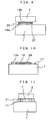
- FIG. 10 in an interconnection construction that at least one of the joining portions is made of a wiring, as shown in FIG. 10, there is a step in level between an electrode pad 12a and an insulator film (passivation film) 17, so that a wiring formed thereon is not flat, thus giving rise to a problem of difficulty in joining of the chips.
- a second insulating layer 38 made of, for example, polyimide can be formed on the insulator film 17 to then form the wiring 18 thereon, in order to flatten the wiring 18, thus giving a merit of facilitating joining.
- the gap between the first and second semiconductor chips 1 and 2 is filled with an insulating resin. That is, after the first and second semiconductor chips 1 and 2 are joined to each other, the insulating resin made of polyimide etc. is dropped into the gap formed therebetween and then hardened to thereby form the underfill (insulating resin layer) 7, as shown in FIG. 11.
- Such an underfill 7 can be formed to bring these chips in contact with each other over the entire surfaces thereof, thus eliminating a problem that the element formed in a semiconductor layer underlying the bump electrode are damaged. That is, during packaging the semiconductor chips with a mold resin, the mold resin cannot easily go into the gap between the semiconductor chips.
- the gap not filled with it causes the resin package 8 to press these semiconductor chips, so that the resultant pressure must be absorbed only by the bump electrode, to give rise to the above-mentioned problem, to solve which problem the underfill 7 can be provided.
- polyimide having an elastic modulus of 4.5GPa
- its elastic modulus is almost equal to that of Au. Since the elastic modulus of the underfill 7 is almost equal to that of the bump electrodes 11 and 21, even after the bump electrodes are melt-adhered and then cooled, the compressive force is evenly applied on and therefore dispersed over the bump electrodes and the other portions of the semiconductor chips, so that it is possible to support the bump electrodes as well as the second semiconductor chip 2 by a surface, thus avoiding a special force from being applied only on the bump electrodes.
- the resin employed as the material of the underfill 7 has a thermal shrinkage factor (thermal expansion coefficient) of 4% or less.
- thermal shrinkage factor thermal expansion coefficient
- such third metal such as, for example, an Au-Sn alloy that melts at a temperature of 300°C or so can be provided on that joining surface and then melted for joining.
- FIG. 12 which shows, like FIG. 6, only the bump electrode as expanded.
- the third metal may be an Au-Sn alloy etc. described later.
- This Au-Sn layer 19 is formed to such a thickness by sputtering, electroless plating, etc.
- the semiconductor chip 1 provided with the Au-Sn layer 19 on the bump electrode 11 can be joined with the second semiconductor chip 2 by, like in the case of the above-mentioned example shown in FIGS. 1A and 1B, putting the first semiconductor device 1 on, for example, a board stage which can be heated and aligning it with the second semiconductor chip 2 superposing the second semiconductor chip 2 thereon with a mounter in such a manner as to align their respective bumps with each other and then heating them to a temperature of 300°C or so under pressure so that the Au-Sn alloy layer 19 may melt and diffuse into Ni of the bump electrodes 11 and 21 to thereby form an intermetallic compound for so-called diffusive joining.
- Au is at least 10 times as large as Sn in diffusion coefficient.
- the bump electrode surface and the Au-Sn alloy layer are intermetallic bonded with each other, they are securely joined to each other at a solder reflow temperature of 260°C or so during the assembling of the semiconductor device.
- the Au-Sn alloy layer in an Au-Sn alloyed state melts near a temperature of 300°C or so but is small in layer thickness, so that it is not peeled off during solder reflowing because it is in the packaged semiconductor device unless an external force is applied on the semiconductor chips. If an external force is applied on it at a high temperature of 300°C or so, the low-melting point alloy layer melts and, therefore, can be peeled off easily.
- the thickness of the Au-Sn alloy layer can be adjusted so that it may not easily peeled off at around a temperature of 300°C.
- the above-mentioned examples have employed Ni as the material of the bump electrodes, Al etc. may be used to thereby diffuse the Au-Sn alloy for diffusive joining similarly. Further, in the construction employed in the above-mentioned examples, the Sn coating may be replaced by an Au-Sn alloy layer. In this case, since Au and the Au-Sn alloy are both Au-based, when the Au-Sn alloy melts, it joins to the Au surface as wetted. That is, although the example shown in FIG.
- the present invention it is possible to join the chips to each other without applying so large load due to the use of supersonic waves during the joining, and also at a relatively low temperature. Accordingly, the semiconductor layers are damaged little, to make it possible to form the circuit elements 31 and 32 also under the joining portion (where the bump electrodes or wirings are formed) as shown in FIG. 16. As a result, the semiconductor chips can be utilized very effectively in area, thus improving the integration density.
- the circuit elements 31 and 32 appear to be in direct contact with the electrode terminal in FIG. 16, typically they are separated from it by an insulating film or partially connected thereto. In FIG. 16, the same components with FIG. 1 are indicated by the same reference numerals and their explanation is omitted. Note here that it is not necessary to form the circuit element in a semiconductor layer under the joining portion on both of the semiconductor chips nor at all of the joining portions.
- the present invention it is unnecessary to heat the chips in a COC type semiconductor device to a high temperature when joining them to each other, to thereby avoid affecting the circuit elements formed on the semiconductor substrate, thus greatly improving the reliability of these elements.
- these semiconductor chips are joined to each other via a metal layer which can be easily separated at a temperature of 300°C or less, even in the case of replacing one of these chips, they are not heated to such an extent that they may be damaged, thus facilitating the replacement greatly.
- the wiring portion when connecting one semiconductor chip to the wiring portion provided on the outermost surface of a passivation film (insulator film) of the other semiconductor chip, the wiring portion can be flattened by interposing an insulating layer between itself and the passivation film, thus facilitating and securing the connection.
- another insulating layer can be interposed between the opposing wiring portions of the respective semiconductor chips to be joined to each other, thus further stabilizing the joining.
- the stress is not concentrated to the semiconductor layer at the joining portion of the electrode terminal but dispersed all over the surfaces thereof, thus improving the reliability of the semiconductor chips.
- the present invention it is possible to improve the reliability of a composite semiconductor device in which its semiconductor circuits are comprised of a plurality of chips like in the case of a combination of, for example, memory elements and the corresponding driver circuits, thus accommodating the requirements for miniaturization and higher functioning of the semiconductor devices.
Landscapes
- Wire Bonding (AREA)
Abstract
Description
Claims (24)
- A semiconductor device comprising:wherein said second metal is made of such a metal that can melt at a temperature lower than a melting point of said first metal and be alloyed with said first metal.a first semiconductor chip having an electrode terminal:a second semiconductor chip having an electrode terminal:a bump electrode made of a first metal for joining said first and second semiconductor chips, said bump electrode being provided on at least one of said electrode terminal of said first semiconductor chip and said electrode terminal of said second semiconductor chip; andan alloy layer formed on a joining portion where said first and second semiconductor chips are joined with each other via said bump electrode, said alloy layer being made of an alloy of said first metal and a second metal,
- A semiconductor device comprising:a first semiconductor chip having an electrode terminal:a second semiconductor chip having an electrode terminal:a bump electrode made of a first metal for joining said first and second semiconductor chips, said bump electrode being provided on at least one of said electrode terminal of said first semiconductor chip and said electrode terminal of said second semiconductor chip; anda third metal layer having a lower melting point than that of said first metal provided on a joining portion where said first and second semiconductor chips are joined with each other via said bump electrode
- A semiconductor device comprising:a first semiconductor chip having an electrode terminal:a second semiconductor chip having an electrode terminal:a bump electrode made of a first metal for joining said first and second semiconductor chips, said bump electrode being provided on at least one of said electrode terminal of said first semiconductor chip and said electrode terminal of said second semiconductor chip; anda detachable material portion provided on a joining portion where said first and second semiconductor chips are joined with each other via said bump electrode, said detachable material being made of such a material that said first and second semiconductor chips can be easily separated from each other at a temperature of 280°C to 500°C.
- The semiconductor device according to claim 1, 2, or 3, wherein said bump electrode is formed on said electrode terminal of each of said first and second semiconductor chips, so that bump electrodes of said first and second semiconductor chips are joined to each other.
- The semiconductor device according to claim 1, 2, or 3, wherein said bump electrode is formed on said electrode terminal of one of said first and second semiconductor chips and a metal layer made of said first metal is formed on said electrode terminal of the other of said first and second semiconductor chips, so that said bump electrode and said electrode terminal are joined to each other.
- The semiconductor device according to any one of claims 1 to 5, wherein a second metal layer made of said second metal or said third metal layer is provided on a right surface and a side surface of said bump electrode made of said first metal, so that said first and second semiconductor chips are joined to each other via said alloy layer or via said third metal layer.
- The semiconductor device according to any one of claims 1 to 6, said joining portion where said first and second semiconductor chips are joined to each other has such a fillet formed thereon that is made of an alloy layer of said first metal and said second metal or said third metal layer.
- The semiconductor device according to claim 1, 4, 5, 6, or 7, wherein said first metal is Au and said second metal is Sn, so that said joining portion has an Au-Sn alloy.
- The semiconductor device according to claim 2, 4, 5, 6, or 7, wherein said third metal is made of an Au-Sn alloy.
- A semiconductor device comprising:wherein said first and second semiconductor chips are electrically interconnected and joined to each other via said low-melting point metal layer so that said electrode terminal or wiring is face to face each other.a first semiconductor chip having an electrode terminal or a wiring;a second semiconductor chip having an electrode terminal or a wiring; anda low-melting point metal layer provided on the surface of said wiring of at least one of said first and second semiconductor chips,
- The semiconductor device according to claim 10, said first and second semiconductor chips are joined to each other with a couple of wirings, and said low-melting point metal layer is provided on a joining portion, further comprising:a first insulating layer provided as interposed at a gap between said a couple of wirings except at said joining portion.
- The semiconductor device according to claim 10 or 11, further comprising:a second insulating layer provided between said wiring and a passivation film on the surface of said semiconductor chip to flatten the surface of said wiring.
- The semiconductor device according to any one of claims 10 to 12, wherein said wiring is made of an Au, which is provided so as to connect to said electrode terminal via a barrier metal layer, and
wherein said low-melting point metal layer is made of an Au-Sn alloy. - The semiconductor device according to any one of claims 10 to 12, wherein said wiring comprising:wherein said low-melting point metal layer is made of an Au-Sn alloy and is provided on said Au wire.a Cu wiring made of Cu formed simultaneously with said electrode terminal;a barrier metal layer provided on said Cu wiring; andan Au wiring provided on said barrier metal layer,
- The semiconductor device according to any one of claims 10 to 13, wherein said wiring is made of Au formed simultaneously with said electrode terminal, and said low-melting point metal layer is made of an Au-Sn alloy.
- The semiconductor device according to claim 7, 8, 12, 13, 14, or 15, wherein said Au-Sn alloy constituting said joining portion has an Au-rich composition containing at least 65 weight-percent of Au.
- The semiconductor device according to claim 7, 8, 12, 13, 14, 15, or 16, wherein an Au-Sn alloy layer of said joining portion has a thickness of 0.8µm or more and 5µm or less.
- The semiconductor device according to any one of claims 1 to 10, further comprising:an insulating resin layer provided at a gap between said first and second semiconductor chips joined each other to fill the gap, said insulating resin layer having nearly the same elastic modulus as said bump electrode.
- The semiconductor device according to any one of claims 1 to 10, further comprising:an insulating resin layer having a thermal shrinkage factor of 5% or less, which is provided at a gap between said first and second semiconductor chips joined each other to fill the gap.
- The semiconductor device according to any one of claims 1 to 19, wherein a circuit element is formed in a semiconductor layer at said joining portion of at least one of said first and second semiconductor chips.
- A method for manufacturing a semiconductor device, in which a first semiconductor chip or substrate and a second semiconductor chip are joined to each other with the surfaces thereof on which an electrode terminal or a wiring are formed respectively as facing each other via metals of the surface of said electrode terminal or said wiring, comprising the steps of:providing at least one of said metals with a low-melting point metal layer having a lower melting point than that of each of said metals; andmelting said low-melting point metal layer or alloying said metals with said low-melting point metal layer to thereby join said first semiconductor chip or substrate and said second semiconductor chip to each other.
- A method for manufacturing a semiconductor device, in which a first semiconductor chip or substrate and a second semiconductor chip are joined to each other with the surfaces thereof on which an electrode terminal or a wiring are formed respectively as facing each other via metals of the surface of said electrode terminal or said wiring, comprising the steps of:providing at least one of said metals with a low-melting point metal layer having a lower melting point than that of each of said metals; andliquefying said low-melting point metal layer to thereby diffuse said metals provided on the surface of said electrode terminal or said wiring into the liquefied low-melting point metal, by the liquid-phase diffusion method, thus joining said first semiconductor chip or substrate and said second semiconductor chip to each other.
- The method according to claim 20, wherein said metals are made of Au and said low-melting point metal layer is made of an Au-Sn alloy or Sn, so that said first semiconductor chip or substrate and said second semiconductor chip are superposed one on the other with said electrode terminals or said wirings thereof as facing each other and heated to a temperature at which said Au-Sn alloy or Sn melts, to be self-aligned and joined with each other.
- The method according to claim 21, 22, or 23, further comprising the steps of:alloying said metals provided on the surface of said electrode terminal or said wiring of one of said first and second semiconductor chips with said low-melting point metal layer provided on the surface thereof; andjoining to the other of said first and second semiconductor chips or substrate.
Applications Claiming Priority (9)
| Application Number | Priority Date | Filing Date | Title |
|---|---|---|---|
| JP2000216298 | 2000-07-17 | ||
| JP2000216298 | 2000-07-17 | ||
| JP2000322926 | 2000-10-23 | ||
| JP2000329926 | 2000-10-23 | ||
| JP2001012648 | 2001-01-22 | ||
| JP2001012648 | 2001-01-22 | ||
| JP2001021113A JP2002289768A (en) | 2000-07-17 | 2001-01-30 | Semiconductor device and its manufacturing method |
| JP2001021113 | 2001-01-30 | ||
| PCT/JP2001/006143 WO2002007219A1 (en) | 2000-07-17 | 2001-07-16 | Semiconductor device and its manufacturing method |
Publications (2)
| Publication Number | Publication Date |
|---|---|
| EP1229583A1 true EP1229583A1 (en) | 2002-08-07 |
| EP1229583A4 EP1229583A4 (en) | 2007-01-03 |
Family
ID=27481457
Family Applications (1)
| Application Number | Title | Priority Date | Filing Date |
|---|---|---|---|
| EP01948030A Withdrawn EP1229583A4 (en) | 2000-07-17 | 2001-07-16 | SEMICONDUCTOR DEVICE AND METHOD FOR MANUFACTURING THE SAME |
Country Status (6)
| Country | Link |
|---|---|
| US (2) | US6734556B2 (en) |
| EP (1) | EP1229583A4 (en) |
| JP (1) | JP2002289768A (en) |
| KR (1) | KR100846270B1 (en) |
| TW (1) | TW518740B (en) |
| WO (1) | WO2002007219A1 (en) |
Families Citing this family (92)
| Publication number | Priority date | Publication date | Assignee | Title |
|---|---|---|---|---|
| TWI313507B (en) * | 2002-10-25 | 2009-08-11 | Megica Corporatio | Method for assembling chips |
| US7242099B2 (en) * | 2001-03-05 | 2007-07-10 | Megica Corporation | Chip package with multiple chips connected by bumps |
| DE60217059T2 (en) * | 2002-02-18 | 2007-06-21 | Stmicroelectronics S.R.L., Agrate Brianza | Mounting structure for an electronic power integrated circuit, which is formed on a semiconductor chip, and a corresponding manufacturing method |
| DE10219353B4 (en) * | 2002-04-30 | 2007-06-21 | Infineon Technologies Ag | Semiconductor device with two semiconductor chips |
| JP4136845B2 (en) | 2002-08-30 | 2008-08-20 | 富士電機ホールディングス株式会社 | Manufacturing method of semiconductor module |
| WO2005086218A1 (en) * | 2004-03-02 | 2005-09-15 | Fuji Electric Holdings Co., Ltd. | Process for producing semiconductor module |
| MXPA05003254A (en) * | 2002-09-24 | 2005-06-08 | Novartis Ag | Sphingosine-1-phosphate receptor agonists in the treatment of demyelinating disorders. |
| JP2004140169A (en) * | 2002-10-17 | 2004-05-13 | Rohm Co Ltd | Package type semiconductor device |
| JP4766831B2 (en) * | 2002-11-26 | 2011-09-07 | 株式会社村田製作所 | Manufacturing method of electronic parts |
| US20050161814A1 (en) * | 2002-12-27 | 2005-07-28 | Fujitsu Limited | Method for forming bumps, semiconductor device and method for manufacturing same, substrate processing apparatus, and semiconductor manufacturing apparatus |
| US7217594B2 (en) * | 2003-02-11 | 2007-05-15 | Fairchild Semiconductor Corporation | Alternative flip chip in leaded molded package design and method for manufacture |
| JP2004288815A (en) * | 2003-03-20 | 2004-10-14 | Seiko Epson Corp | Semiconductor device and its manufacturing method |
| JP2005011838A (en) * | 2003-06-16 | 2005-01-13 | Toshiba Corp | Semiconductor device and its assembling method |
| FI20031341L (en) | 2003-09-18 | 2005-03-19 | Imbera Electronics Oy | Method for manufacturing an electronic module |
| US8641913B2 (en) | 2003-10-06 | 2014-02-04 | Tessera, Inc. | Fine pitch microcontacts and method for forming thereof |
| US7495179B2 (en) | 2003-10-06 | 2009-02-24 | Tessera, Inc. | Components with posts and pads |
| US20050098605A1 (en) * | 2003-11-06 | 2005-05-12 | International Business Machines Corporation | Apparatus and method for low pressure wirebond |
| US7394161B2 (en) | 2003-12-08 | 2008-07-01 | Megica Corporation | Chip structure with pads having bumps or wirebonded wires formed thereover or used to be tested thereto |
| US7709968B2 (en) | 2003-12-30 | 2010-05-04 | Tessera, Inc. | Micro pin grid array with pin motion isolation |
| JP4552934B2 (en) * | 2004-03-02 | 2010-09-29 | 富士電機ホールディングス株式会社 | Electronic component mounting method |
| KR100543729B1 (en) * | 2004-03-24 | 2006-01-20 | 아바고테크놀로지스코리아 주식회사 | High frequency module package with high heat dissipation efficiency and reduced thickness and size and assembly method |
| US9318428B2 (en) * | 2004-05-28 | 2016-04-19 | Nxp B.V. | Chip having two groups of chip contacts |
| JP4718809B2 (en) | 2004-08-11 | 2011-07-06 | ローム株式会社 | Electronic device, semiconductor device using the same, and method for manufacturing semiconductor device |
| JP4453498B2 (en) * | 2004-09-22 | 2010-04-21 | 富士電機システムズ株式会社 | Power semiconductor module and manufacturing method thereof |
| US11842972B2 (en) | 2004-09-28 | 2023-12-12 | Rohm Co., Ltd. | Semiconductor device with a semiconductor chip connected in a flip chip manner |
| JP2006100385A (en) | 2004-09-28 | 2006-04-13 | Rohm Co Ltd | Semiconductor device |
| JP2006100552A (en) * | 2004-09-29 | 2006-04-13 | Rohm Co Ltd | Wiring board and semiconductor device |
| US7454605B2 (en) | 2004-11-18 | 2008-11-18 | International Business Machines Corporation | Method for adapter code image update |
| JP4908750B2 (en) * | 2004-11-25 | 2012-04-04 | ローム株式会社 | Semiconductor device |
| US7956460B2 (en) * | 2004-12-28 | 2011-06-07 | Rohm Co., Ltd. | Semiconductor chip and method for manufacturing same, electrode structure of semiconductor chip and method for forming same, and semiconductor device |
| US8294279B2 (en) * | 2005-01-25 | 2012-10-23 | Megica Corporation | Chip package with dam bar restricting flow of underfill |
| JP4891556B2 (en) * | 2005-03-24 | 2012-03-07 | 株式会社東芝 | Manufacturing method of semiconductor device |
| US7781886B2 (en) * | 2005-06-14 | 2010-08-24 | John Trezza | Electronic chip contact structure |
| US8456015B2 (en) | 2005-06-14 | 2013-06-04 | Cufer Asset Ltd. L.L.C. | Triaxial through-chip connection |
| US7838997B2 (en) | 2005-06-14 | 2010-11-23 | John Trezza | Remote chip attachment |
| US7946331B2 (en) | 2005-06-14 | 2011-05-24 | Cufer Asset Ltd. L.L.C. | Pin-type chip tooling |
| US7560813B2 (en) | 2005-06-14 | 2009-07-14 | John Trezza | Chip-based thermo-stack |
| US7851348B2 (en) | 2005-06-14 | 2010-12-14 | Abhay Misra | Routingless chip architecture |
| US7687400B2 (en) | 2005-06-14 | 2010-03-30 | John Trezza | Side stacking apparatus and method |
| US7215032B2 (en) | 2005-06-14 | 2007-05-08 | Cubic Wafer, Inc. | Triaxial through-chip connection |
| US7786592B2 (en) | 2005-06-14 | 2010-08-31 | John Trezza | Chip capacitive coupling |
| FI119714B (en) | 2005-06-16 | 2009-02-13 | Imbera Electronics Oy | PCB design and method of manufacturing PCB design |
| US7569926B2 (en) * | 2005-08-26 | 2009-08-04 | Innovative Micro Technology | Wafer level hermetic bond using metal alloy with raised feature |
| JP4380618B2 (en) * | 2005-10-21 | 2009-12-09 | 株式会社デンソー | Sensor device |
| JP4450230B2 (en) * | 2005-12-26 | 2010-04-14 | 株式会社デンソー | Semiconductor device |
| US20070205253A1 (en) * | 2006-03-06 | 2007-09-06 | Infineon Technologies Ag | Method for diffusion soldering |
| JP4580881B2 (en) * | 2006-03-08 | 2010-11-17 | 株式会社住友金属エレクトロデバイス | Rectangular metal ring brazing method |
| US7687397B2 (en) | 2006-06-06 | 2010-03-30 | John Trezza | Front-end processed wafer having through-chip connections |
| US7713782B2 (en) * | 2006-09-22 | 2010-05-11 | Stats Chippac, Inc. | Fusible I/O interconnection systems and methods for flip-chip packaging involving substrate-mounted stud-bumps |
| US9847309B2 (en) | 2006-09-22 | 2017-12-19 | STATS ChipPAC Pte. Ltd. | Semiconductor device and method of forming vertical interconnect structure between semiconductor die and substrate |
| US7670874B2 (en) * | 2007-02-16 | 2010-03-02 | John Trezza | Plated pillar package formation |
| US7748116B2 (en) * | 2007-04-05 | 2010-07-06 | John Trezza | Mobile binding in an electronic connection |
| TWI364793B (en) * | 2007-05-08 | 2012-05-21 | Mutual Pak Technology Co Ltd | Package structure for integrated circuit device and method of the same |
| US7939939B1 (en) * | 2007-06-11 | 2011-05-10 | Texas Instruments Incorporated | Stable gold bump solder connections |
| US20090020876A1 (en) * | 2007-07-20 | 2009-01-22 | Hertel Thomas A | High temperature packaging for semiconductor devices |
| JP5629580B2 (en) * | 2007-09-28 | 2014-11-19 | テッセラ,インコーポレイテッド | Flip chip interconnect with double posts |
| KR100908648B1 (en) * | 2007-10-19 | 2009-07-21 | (주)에스엠엘전자 | Multi-layer bump structure and its manufacturing method |
| JP2009158593A (en) * | 2007-12-25 | 2009-07-16 | Tessera Interconnect Materials Inc | Bump structure and manufacturing method thereof |
| US20100084755A1 (en) * | 2008-10-08 | 2010-04-08 | Mark Allen Gerber | Semiconductor Chip Package System Vertical Interconnect |
| KR101332532B1 (en) * | 2008-11-28 | 2013-11-22 | 후지쯔 가부시끼가이샤 | Electronic device manufacturing method, substrate for mounting electronic component and method for manufacturing substrate for mounting semicomductor device |
| US8637983B2 (en) * | 2008-12-19 | 2014-01-28 | Ati Technologies Ulc | Face-to-face (F2F) hybrid structure for an integrated circuit |
| WO2010132717A1 (en) * | 2009-05-13 | 2010-11-18 | The Regents Of The University Of California | High density non-volatile information storage |
| FI20095557A0 (en) | 2009-05-19 | 2009-05-19 | Imbera Electronics Oy | Manufacturing process and electronics module with new wiring possibilities |
| JP5273073B2 (en) * | 2010-03-15 | 2013-08-28 | オムロン株式会社 | Electrode structure and micro device package having the electrode structure |
| US8330272B2 (en) * | 2010-07-08 | 2012-12-11 | Tessera, Inc. | Microelectronic packages with dual or multiple-etched flip-chip connectors |
| US8580607B2 (en) | 2010-07-27 | 2013-11-12 | Tessera, Inc. | Microelectronic packages with nanoparticle joining |
| US8853558B2 (en) | 2010-12-10 | 2014-10-07 | Tessera, Inc. | Interconnect structure |
| JP4778120B1 (en) * | 2011-03-08 | 2011-09-21 | 有限会社ナプラ | Electronics |
| TWI467718B (en) * | 2011-12-30 | 2015-01-01 | 財團法人工業技術研究院 | Bump structure and electronic package contact structure and manufacturing method thereof |
| CN102543908A (en) * | 2012-01-05 | 2012-07-04 | 三星半导体(中国)研究开发有限公司 | Flip chip encapsulating piece and manufacturing method thereof |
| CN102543939B (en) * | 2012-01-05 | 2015-09-16 | 三星半导体(中国)研究开发有限公司 | The lamination flip chip packaging structure of ultra fine-pitch pad and manufacture method thereof |
| JP2014049733A (en) * | 2012-09-04 | 2014-03-17 | Fujitsu Semiconductor Ltd | Semiconductor device and semiconductor device manufacturing method |
| US8963311B2 (en) * | 2012-09-26 | 2015-02-24 | Apple Inc. | PoP structure with electrically insulating material between packages |
| CN103779351B (en) * | 2012-10-23 | 2017-11-07 | 格科微电子(上海)有限公司 | Three-dimension packaging structure and its manufacture method |
| KR101420514B1 (en) * | 2012-10-23 | 2014-07-17 | 삼성전기주식회사 | Substrate structure having electronic components and method of manufacturing substrate structure having electronic components |
| CN112264086A (en) | 2013-04-29 | 2021-01-26 | 沙特基础工业公司 | Catalytic process for the conversion of naphtha to olefins |
| KR102123039B1 (en) * | 2013-07-19 | 2020-06-15 | 니치아 카가쿠 고교 가부시키가이샤 | Light emitting device and method of manufacturing the same |
| KR101430673B1 (en) * | 2013-11-05 | 2014-08-19 | 주식회사 케이이씨 | Semiconductor device and die bonding structure thereof |
| US20150318254A1 (en) * | 2013-12-17 | 2015-11-05 | Oracle International Corporation | Electroplated solder with eutectic chemical composition |
| JP6379650B2 (en) * | 2014-05-12 | 2018-08-29 | 富士通株式会社 | Manufacturing method of semiconductor device |
| US10568213B2 (en) | 2014-07-31 | 2020-02-18 | Skyworks Solutions, Inc. | Multilayered transient liquid phase bonding |
| US20160308100A1 (en) * | 2015-04-17 | 2016-10-20 | Chipmos Technologies Inc | Semiconductor package and method of manufacturing thereof |
| US10886250B2 (en) | 2015-07-10 | 2021-01-05 | Invensas Corporation | Structures and methods for low temperature bonding using nanoparticles |
| US9633971B2 (en) | 2015-07-10 | 2017-04-25 | Invensas Corporation | Structures and methods for low temperature bonding using nanoparticles |
| US10103095B2 (en) * | 2016-10-06 | 2018-10-16 | Compass Technology Company Limited | Fabrication process and structure of fine pitch traces for a solid state diffusion bond on flip chip interconnect |
| US11069606B2 (en) | 2016-10-06 | 2021-07-20 | Compass Technology Company Limited | Fabrication process and structure of fine pitch traces for a solid state diffusion bond on flip chip interconnect |
| TWI892323B (en) | 2016-10-27 | 2025-08-01 | 美商艾德亞半導體科技有限責任公司 | Structures and methods for low temperature bonding |
| US10439587B2 (en) * | 2016-12-02 | 2019-10-08 | Skyworks Solutions, Inc. | Methods of manufacturing electronic devices formed in a cavity |
| CN115315356B (en) | 2020-03-31 | 2023-11-21 | 京瓷株式会社 | Thermal head and thermal printer |
| US12211809B2 (en) | 2020-12-30 | 2025-01-28 | Adeia Semiconductor Bonding Technologies Inc. | Structure with conductive feature and method of forming same |
| CN114823556A (en) * | 2022-03-29 | 2022-07-29 | 成都奕斯伟系统技术有限公司 | Semiconductor package and method of forming the same |
| JPWO2023228811A1 (en) * | 2022-05-25 | 2023-11-30 |
Family Cites Families (23)
| Publication number | Priority date | Publication date | Assignee | Title |
|---|---|---|---|---|
| JPS57178814A (en) * | 1981-04-30 | 1982-11-04 | Kuraray Co Ltd | Manufacture of molded resin molding and mold therefor |
| US4875617A (en) * | 1987-01-20 | 1989-10-24 | Citowsky Elya L | Gold-tin eutectic lead bonding method and structure |
| JP2626001B2 (en) | 1988-12-13 | 1997-07-02 | 富士通株式会社 | Fluxless joining method |
| JP2546407B2 (en) * | 1990-03-27 | 1996-10-23 | 日本電気株式会社 | Hybrid element and manufacturing method thereof |
| US5280414A (en) * | 1990-06-11 | 1994-01-18 | International Business Machines Corp. | Au-Sn transient liquid bonding in high performance laminates |
| US5346857A (en) * | 1992-09-28 | 1994-09-13 | Motorola, Inc. | Method for forming a flip-chip bond from a gold-tin eutectic |
| AU689448B2 (en) | 1992-10-01 | 1998-04-02 | Schering Corporation | Use of IL-10 to prevent or treat insulin-dependent diabetes mellitus |
| DE69426090T2 (en) * | 1993-04-27 | 2001-03-01 | Nec Corp., Tokio/Tokyo | Method of manufacturing an optical semiconductor device |
| JP3348528B2 (en) * | 1994-07-20 | 2002-11-20 | 富士通株式会社 | Method for manufacturing semiconductor device, method for manufacturing semiconductor device and electronic circuit device, and electronic circuit device |
| JP3233535B2 (en) * | 1994-08-15 | 2001-11-26 | 株式会社東芝 | Semiconductor device and manufacturing method thereof |
| US5864178A (en) * | 1995-01-12 | 1999-01-26 | Kabushiki Kaisha Toshiba | Semiconductor device with improved encapsulating resin |
| US5659203A (en) * | 1995-06-07 | 1997-08-19 | International Business Machines Corporation | Reworkable polymer chip encapsulant |
| US5796591A (en) * | 1995-06-07 | 1998-08-18 | International Business Machines Corporation | Direct chip attach circuit card |
| JPH098046A (en) | 1995-06-20 | 1997-01-10 | Nippon Avionics Co Ltd | Method for forming protruding electrode of semiconductor chip |
| JPH0997791A (en) * | 1995-09-27 | 1997-04-08 | Internatl Business Mach Corp <Ibm> | Bump structure, bump forming method, mounted connection body |
| DE19531158A1 (en) * | 1995-08-24 | 1997-02-27 | Daimler Benz Ag | Diffusion soldering method esp. for semiconductor components |
| JPH09102514A (en) * | 1995-10-05 | 1997-04-15 | Nippon Telegr & Teleph Corp <Ntt> | Bump bonding method and bump bonding structure |
| JPH09213702A (en) | 1996-01-31 | 1997-08-15 | Sony Corp | Semiconductor device and method of mounting semiconductor device |
| JPH09326465A (en) | 1996-06-06 | 1997-12-16 | Matsushita Electric Ind Co Ltd | Semiconductor device and manufacturing method thereof |
| DE19640192A1 (en) * | 1996-09-30 | 1998-04-02 | Bosch Gmbh Robert | Process for flip chip assembly |
| JP3324446B2 (en) * | 1997-05-22 | 2002-09-17 | 松下電器産業株式会社 | Mounting structure and mounting method of chip with bump |
| JP2001510944A (en) * | 1997-07-21 | 2001-08-07 | アギラ テクノロジーズ インコーポレイテッド | Semiconductor flip chip package and method of manufacturing the same |
| JP4009380B2 (en) | 1999-02-18 | 2007-11-14 | ローム株式会社 | Manufacturing method of semiconductor chip |
-
2001
- 2001-01-30 JP JP2001021113A patent/JP2002289768A/en active Pending
- 2001-07-16 EP EP01948030A patent/EP1229583A4/en not_active Withdrawn
- 2001-07-16 WO PCT/JP2001/006143 patent/WO2002007219A1/en not_active Ceased
- 2001-07-16 KR KR1020027003517A patent/KR100846270B1/en not_active Expired - Fee Related
- 2001-07-16 US US10/088,163 patent/US6734556B2/en not_active Expired - Lifetime
- 2001-07-17 TW TW090117398A patent/TW518740B/en not_active IP Right Cessation
-
2004
- 2004-03-10 US US10/795,994 patent/US7384863B2/en not_active Expired - Lifetime
Also Published As
| Publication number | Publication date |
|---|---|
| WO2002007219A1 (en) | 2002-01-24 |
| US6734556B2 (en) | 2004-05-11 |
| EP1229583A4 (en) | 2007-01-03 |
| TW518740B (en) | 2003-01-21 |
| KR20020030116A (en) | 2002-04-22 |
| US20040169286A1 (en) | 2004-09-02 |
| JP2002289768A (en) | 2002-10-04 |
| US7384863B2 (en) | 2008-06-10 |
| US20020149117A1 (en) | 2002-10-17 |
| KR100846270B1 (en) | 2008-07-16 |
Similar Documents
| Publication | Publication Date | Title |
|---|---|---|
| US6734556B2 (en) | Semiconductor device with chip-on-chip construction joined via a low-melting point metal layer | |
| JP3127151B2 (en) | Solder structure, electronic component assembly, and method of manufacturing electronic component assembly | |
| US8101514B2 (en) | Semiconductor device having elastic solder bump to prevent disconnection | |
| US6250541B1 (en) | Method of forming interconnections on electronic modules | |
| JP3262497B2 (en) | Chip mounted circuit card structure | |
| US7939939B1 (en) | Stable gold bump solder connections | |
| US8133761B2 (en) | Packaged system of semiconductor chips having a semiconductor interposer | |
| US20030210531A1 (en) | Method of forming an apparatus to reduce thermal fatigue stress on flip chip solder connections | |
| US6781247B2 (en) | Semiconductor device | |
| JP4076841B2 (en) | Manufacturing method of semiconductor device | |
| JPWO1998040915A1 (en) | Electronic components and semiconductor devices, their manufacturing methods, circuit boards on which they are mounted, and electronic equipment having such circuit boards | |
| US20040222522A1 (en) | Semiconductor device and manufacturing method of the same | |
| US20020031904A1 (en) | Semiconductor device and method for manufacturing the same | |
| JPH11354677A (en) | Semiconductor device mounting structure and mounting method | |
| JPH10173006A (en) | Semiconductor device and method of manufacturing semiconductor device | |
| KR100367314B1 (en) | Semiconductor device and method of fabricating the same | |
| JP4011214B2 (en) | Semiconductor device and joining method using solder | |
| JP3582014B2 (en) | Semiconductor pellet mounting method | |
| US6649833B1 (en) | Negative volume expansion lead-free electrical connection | |
| JPWO1997003465A1 (en) | Semiconductor pellet, its mounting method, and bump electrode | |
| JPH11126852A (en) | Semiconductor device, method of manufacturing the same, and method of mounting conductive ball | |
| JPH11260964A (en) | Semiconductor package | |
| JP2003092307A (en) | Semiconductor device |
Legal Events
| Date | Code | Title | Description |
|---|---|---|---|
| PUAI | Public reference made under article 153(3) epc to a published international application that has entered the european phase |
Free format text: ORIGINAL CODE: 0009012 |
|
| AK | Designated contracting states |
Kind code of ref document: A1 Designated state(s): DE FR GB |
|
| 17P | Request for examination filed |
Effective date: 20020711 |
|
| RIC1 | Information provided on ipc code assigned before grant |
Ipc: H01L 21/60 20060101AFI20060725BHEP Ipc: H01L 23/485 20060101ALI20060725BHEP |
|
| A4 | Supplementary search report drawn up and despatched |
Effective date: 20061204 |
|
| RIC1 | Information provided on ipc code assigned before grant |
Ipc: H01L 23/485 20060101ALI20061128BHEP Ipc: H01L 25/065 20060101ALI20061128BHEP Ipc: H01L 21/60 20060101AFI20060725BHEP Ipc: H01L 21/56 20060101ALI20061128BHEP |
|
| 17Q | First examination report despatched |
Effective date: 20090420 |
|
| STAA | Information on the status of an ep patent application or granted ep patent |
Free format text: STATUS: THE APPLICATION IS DEEMED TO BE WITHDRAWN |
|
| 18D | Application deemed to be withdrawn |
Effective date: 20120201 |