EP1227669A2 - Image sensing apparatus, shading correction method, program, and storage medium - Google Patents
Image sensing apparatus, shading correction method, program, and storage medium Download PDFInfo
- Publication number
- EP1227669A2 EP1227669A2 EP02250153A EP02250153A EP1227669A2 EP 1227669 A2 EP1227669 A2 EP 1227669A2 EP 02250153 A EP02250153 A EP 02250153A EP 02250153 A EP02250153 A EP 02250153A EP 1227669 A2 EP1227669 A2 EP 1227669A2
- Authority
- EP
- European Patent Office
- Prior art keywords
- shading correction
- image sensing
- sensing element
- correction coefficients
- pixel
- Prior art date
- Legal status (The legal status is an assumption and is not a legal conclusion. Google has not performed a legal analysis and makes no representation as to the accuracy of the status listed.)
- Granted
Links
Images




Classifications
-
- H—ELECTRICITY
- H04—ELECTRIC COMMUNICATION TECHNIQUE
- H04N—PICTORIAL COMMUNICATION, e.g. TELEVISION
- H04N23/00—Cameras or camera modules comprising electronic image sensors; Control thereof
- H04N23/60—Control of cameras or camera modules
- H04N23/66—Remote control of cameras or camera parts, e.g. by remote control devices
- H04N23/663—Remote control of cameras or camera parts, e.g. by remote control devices for controlling interchangeable camera parts based on electronic image sensor signals
-
- H—ELECTRICITY
- H04—ELECTRIC COMMUNICATION TECHNIQUE
- H04N—PICTORIAL COMMUNICATION, e.g. TELEVISION
- H04N25/00—Circuitry of solid-state image sensors [SSIS]; Control thereof
- H04N25/60—Noise processing, e.g. detecting, correcting, reducing or removing noise
- H04N25/63—Noise processing, e.g. detecting, correcting, reducing or removing noise applied to dark current
-
- H—ELECTRICITY
- H04—ELECTRIC COMMUNICATION TECHNIQUE
- H04N—PICTORIAL COMMUNICATION, e.g. TELEVISION
- H04N25/00—Circuitry of solid-state image sensors [SSIS]; Control thereof
- H04N25/60—Noise processing, e.g. detecting, correcting, reducing or removing noise
- H04N25/68—Noise processing, e.g. detecting, correcting, reducing or removing noise applied to defects
Definitions
- the present invention relates to an image sensing apparatus, shading correction method, and storage medium and, more particularly, to an image sensing apparatus that uses an exchangeable image sensing lens, a shading correction method applied to the image sensing apparatus, and a storage medium that stores a program for implementing the shading correction method.
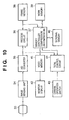
- Fig. 10 is a block diagram showing an example of the arrangement of a conventional lens-exchangeable digital still camera.
- a camera operation switch 43 comprises a main SW and release SW.
- a total control circuit 44 detects a change in state of the camera operation switch 43, and starts power supply to other circuit blocks.
- An object image within a photographing frame range forms on an image sensing unit 34 via a main photographing optical system 33, and the image sensing unit 34 outputs an electrical signal to an A/D converter 35.
- the electrical signal is converted in turn into a predetermined digital signal for each pixel, and the digital signal is sent to a process circuit 36.
- the process circuit 36 generates R, G, and B color signals based on pixel data, and periodically transfers the generation results for each frame to a video memory 41 via a memory controller 37 while the photographer performs pre-photographing operation.
- a monitor display 42 makes viewfinder display and the like based on the data transferred to the video memory 41.
- pixel data for one frame output from the process circuit 36 are stored in a frame memory 38 in response to a control signal from the total control circuit 44 that detects a change in state of the camera operation switch 43. Subsequently, the data in the frame memory 38 is compressed by the memory controller 37 and a work memory 39 in a predetermined compression format, and the compression result is stored in an external memory 40.
- the external memory 40 comprises a nonvolatile memory such as a flash memory or the like.
- the memory controller 37 decompresses the compressed data stored in the external memory 40 to normal data for respective photographing pixels, and transfers the decompression result to the video memory 41.
- the monitor display 42 makes viewfinder display and the like based on the data transferred to the video memory 41.
- An image sensing element used in such conventional lens-exchangeable digital camera uses microlenses shown in Figs. 11A and 11B for respective photosensitive pixels of the image sensing element so as to improve photosensitivity for each pixel.
- Figs. 11A and 11B show the principle of shading (spatial sensitivity nonuniformity depending on the incident angle of incoming light from a lens) produced depending on the relationship between the microlens position and the angle of incoming light from the lens.
- reference numeral 20 denotes a lens as a field lens; 21, microlenses; and 22, photosensitive portions of the image sensing element.
- microlenses 21 are provided for respective photosensitive portions 22 of the pixels of the image sensing element, even when each photosensitive portion 22 of the image sensing element has a narrow effective sensitivity region, marginal light can be effectively focused on the photosensitive portion 22.
- Such light amount drop is normally called white shading. This phenomenon becomes conspicuous as the pixel position on the image sensing element separates farther away from the optical axis of the lens 20.
- a method of correcting white shading generated by a combination of the lens 20 and microlenses 21 on the image sensing element is disclosed in, e.g., Japanese Patent Laid-Open No. 6-197266.
- shading correction data is stored in advance in an internal memory of a lens, and is read out upon photographing.
- a reference voltage of an analog/digital conversion circuit is generated based on the readout data, and an analog sensed image signal is converted into a digital signal based on this reference voltage, thus implementing shading correction.
- the conventional lens-exchangeable digital camera uses the same optical system (e.g., an exchangeable lens system) as that in a conventional single-lens reflex silver halide film camera, it requires an image sensing element with a size considerably larger than that of an image sensing element of a digital camera that cannot use such optical system.
- an exchangeable lens system e.g., an exchangeable lens system
- a recent solid-state image sensing element comprises the microlenses 21 for focusing incoming light onto photodiodes (photosensitive portions 22 of the image sensing element) to improve sensitivity.
- photodiodes photosensitive portions 22 of the image sensing element
- the incident angle of incoming light becomes large, the incoming light refracted by the microlens 21 is focused at a position separated away from the center of each photodiode, thus decreasing the sensitivity of that pixel.
- an image sensing apparatus that makes shading correction in consideration of an increase in incident angle of incoming light on the peripheral portion of the image sensing element due to the characteristics of the lens that forms an object image is available, as disclosed in Japanese Patent Laid-Open No. 6-197266.
- the incident angle characteristics of incoming light rays to the image sensing element change drastically upon exchanging lenses, and shading correction cannot be accurately done.
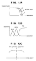
- Figs. 12A to 12C show the generation principle of color shading due to multi-layered type reflective infrared cut filters.
- Fig. 12A shows spectral transmission characteristics of the reflective infrared cut filters depending on the incident angles
- Fig. 12B shows an example of spectral sensitivity characteristics of an image sensing element which comprises on-chip color filters
- Fig. 12C shows the sensitivity of a red filter pixel.
- Figs. 12A to 12C exemplify an image sensing element which has RGB primary color type on-chip color filters. Note that the wavelength on the abscissa of Fig. 12A has the same level scale as that of the wavelength on the abscissa of Fig. 12B.
- the spectral transmission characteristics of the infrared cut filters have no dependence on incident angle in the wavelength ranges of blue and green color filters, but have large dependence on incident angle in the wavelength range of a red color filter.
- the sensitivity characteristics of a signal output from the image sensing element are expressed by the product of the spectral transmission characteristics of the infrared cut filters and the spectral sensitivity characteristics of the image sensing element.
- the present invention has been made in consideration of the aforementioned problems, and has as a concern provide an image sensing apparatus, shading correction method, and storage medium, which can remove sensitivity nonuniformity on the image sensing element plane irrespective of exchange of lenses in an image sensing apparatus which uses an exchangeable lens.
- an image sensing apparatus is characterized by the following arrangement.
- an image sensing apparatus which comprises an image sensing element and can exchange a lens, comprises storage means for storing shading correction coefficients respectively corresponding to pixels of the image sensing element, and correction means for making a correction calculation of pixel data read out from each pixel of the image sensing element by extracting the shading correction coefficient associated with the corresponding pixel from the shading correction coefficients stored in the storage means, and the storage means independently stores the shading correction coefficients in correspondence with pixels which are influenced by a color filter, which does not transmit a specific wavelength range and is inserted between the lens and the image sensing element, and pixels which are not influenced by the color filter.
- a shading correction method according to the present invention is characterized by the following arrangement.
- a shading correction method applied to an image sensing apparatus comprises the correction step of making a correction calculation of pixel data read out from each pixel of the image sensing element by extracting the shading correction coefficient associated with the corresponding pixel from shading correction coefficients stored in storage means which stores shading correction coefficients respectively corresponding to pixels of the image sensing element, and the shading correction coefficients are independently stored in the storage means in correspondence with pixels which are influenced by a color filter, which does not transmit a specific wavelength range and is inserted between the lens and the image sensing element, and pixels which are not influenced by the color filter.
- a program according to the present invention is characterized by the following arrangement.
- a program makes a computer implement the shading correction method.
- a storage medium according to the present invention is characterized by the following arrangement.
- a storage medium computer-readably stores the
- Fig. 1 is a block diagram showing the arrangement of an image sensing apparatus (digital still camera) according to an embodiment of the present invention.
- This image sensing apparatus can exchange lenses.
- reference numeral 1 denotes a total control CPU for controlling the overall camera; 2, an exit pupil position detector; and 3, an exchangeable lens.
- the exchangeable lens 3 includes exit pupil position information, and the detector 2 detects the exit pupil position information included in the exchangeable lens 3, generates encode information by correcting the detected value, and outputs the generated information to the CPU 1.
- the exit pupil position information is used to calculate shading correction coefficients, as will be described later.
- the exit pupil position information is corrected according to at least one of the zoom position, focus position, image height, and aperture value of the exchangeable lens 3. More specifically, the exit pupil position is normally expressed by the distance between a lens and image sensing element on the optical axis, and changes in synchronism with a change in zoom or focus position.
- the exit pupil position slightly changes when the image height (the distance between the position of a pixel of interest and a point on the optical axis on the image sensing element plane) changes.
- the aperture value changes, the range of the incident angle of light that strikes the pixel of interest of the image sensing element changes. Since these changes appear as errors upon calculating the shading correction coefficients, the exit pupil position information of the exchangeable lens 3 is corrected in accordance with at least one of the zoom position, focus position, image height, and aperture value of the exchangeable lens 3, so as to attain accurate shading correction.
- Reference numeral 4 denotes multi-layered reflection type infrared cut filters; and 5, an image sensing element.
- the image sensing element 5 comprises, e.g., a charge transfer element such as a CCD or the like.
- An object image is formed on the image sensing element 5 via the exchangeable lens 3, and the image sensing element 5 reads out charges accumulated as a result of image formation in turn for respective pixels and outputs them to a CDS/AGC circuit 6.
- the CDS/AGC circuit 6 suppresses noise components such as reset noise and the like generated in the image sensing element 5, then amplifies the charge signals to an appropriate level, and outputs these signals to an A/D conversion circuit 7.
- the A/D conversion circuit 7 converts luminance data of the object corresponding to the above charge amount into digital data. Since optical color filters used to generate color signals (e.g., R, G, and B signals) are adhered onto the image sensing element 5, the output signals from the image sensing element 5 indicate respective colors in turn.
- Reference numeral 8 denotes a driver for supplying electric energy required to accumulate charges on respective elements of the image sensing element 5 to those elements. More specifically, the driver 8 supplies electric energy by scanning the image sensing element 5 two-dimensionally on the basis of timing signals sent from a timing generator 9.
- the timing generator 9 supplies a horizontal sync signal HD and vertical sync signal VD to an address generation circuit 10, which generates address signals based on these sync signals.
- Reference numerals 12 to 15 denote memories for storing correction data required to make sensitivity correction (shading correction) of the image sensing element 5 (to be described later): reference numeral 12 denotes an H memory H1 that stores first horizontal correction data; 13, an H memory H2 that stores second horizontal correction data; 14, a V memory V1 that stores first vertical correction data; and 15, a V memory V2 that stores second vertical correction data.
- An address discrimination circuit 11 outputs predetermined signals HSEL and VSEL on the basis of the address signals output from the address generation circuit 10.
- Reference numerals 16 and 17 denote selectors for selecting from the output signals sent from the memories 12 to 15 on the basis of the predetermined signals HSEL and VSEL sent from the address discrimination circuit 11, and outputting horizontal and vertical correction data.
- Reference numeral 18 denotes a multiplier circuit MUL1 for multiplying output levels for respective pixels output from the A/D conversion circuit 7 by the horizontal correction data obtained via the selector 16.
- Reference numeral 19 denotes a multiplier circuit MUL2 for multiplying the outputs from the multiplier circuit (MUL1) 18 by the vertical correction data obtained via the selector 17.
- Pixel data which have undergone sensitivity correction (shading correction) and are output from the multiplier circuit (MUL2) 19, are normally sent to a process circuit (not shown), and then undergo dark level correction, ⁇ conversion, and a color interpolation process.
- the processing result is stored in a memory (not shown).
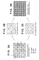
- Figs. 2A to 2D show the color interpolation process.
- Fig. 2A shows a pixel matrix of the image sensing element 5
- Fig. 2B shows a G (green) interpolation filter
- Fig. 2C shows an R (red)/B (blue) interpolation filter
- Fig. 2D shows a pixel matrix after the interpolation process.
- the color filter matrices used in the image sensing element are general Bayer matrices, which include a staggered matrix for G, as shown in Fig. 2B, and a line sequential matrix for R/B, as shown in Fig. 2C.
- G interpolation filter coefficients For example, in order to generate a G interpolated signal of pixel a shown in Fig. 2A, data of pixel a and its eight surrounding pixels bounded by dotted line a1 are multiplied by G interpolation filter coefficients, and the products are added up.
- G interpolation filter shown in Fig. 2B coefficients corresponding to G (green) pixels within dotted line a1 are "1" at the position of pixel a, and "0" at the positions of pixels at four corners.
- data of pixel a directly becomes the G interpolated signal.
- the G interpolated signal of pixel b is a value obtained by adding up products after multiplication of the coefficients at the upper, lower, right, and left neighboring positions.
- the G interpolated signal in this case is the average value of luminance data at the upper, lower, right, and left neighboring positions.
- R/B interpolated signals for all R (red)/B (blue) pixels are determined using R/B interpolation filters having different coefficients from those of the G interpolation filter.
- sensitivity correction shading correction
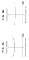
- Figs. 3A and 3B show shading correction coefficients used to correct shading produced due to a combination of the lens and image sensing element device structure.
- the exit pupil position detector 2 shown in Fig. 1 reads out exit pupil position information in the exchangeable lens 3, corrects it in accordance with the zoom position, focus position, or the like, and sends the corrected information to the total control CPU 1, which calculates shading correction coefficients in accordance with the corrected exit pupil position information.
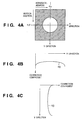
- shading correction coefficients are determined strictly in correspondence with the image height, they must be set in a concentric pattern having the image sensing element as the center, thus making a hardware process difficult. Hence, in this embodiment, shading correction coefficients shown in Figs. 4A to 4C are set.
- Figs. 4A to 4C show shading correction coefficients in this embodiment.
- Fig. 4A shows the plane of the image sensing element
- Fig. 4B shows horizontal shading correction coefficient components
- Fig. 4C shows vertical shading correction coefficient components.
- shading correction coefficients are set to increase sensitivity for the right and left peripheral portions of the image sensing element, which have low sensitivity, in the horizontal direction
- shading correction coefficients are set to increase sensitivity for the upper and lower peripheral portions of the image sensing element, which have low sensitivity, in the vertical direction, so that when the horizontal and vertical shading correction coefficients are multiplied each other on the image plane, pseudo concentric correction is done.
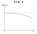
- This pseudo concentric correction can assure sufficiently satisfactory precision compared to concentric correction if the sensitivity changes sufficiently slowly with respect to the incident angle of incoming light to the image sensing element, and a change in sensitivity is small, as shown in Fig. 6 (to be described later).
- Fig. 5 shows an optical path from the lens to the image sensing element.
- reference numeral 20 denotes a lens; and 23, a stop.
- ⁇ represents the incident angle of light
- d represents the distance of light that becomes incident on the image sensing element 5 from the center of the optical axis, i.e., the image height
- p is the distance between the lens 20 and image sensing element 5 on the optical axis, i.e., the exit pupil position.
- Fig. 6 is a graph showing sensitivity with respect to the incident angle ⁇
- Fig. 7 shows X- and Y-components of the image height d on the plane of the image sensing element 5.
- sensitivity y (Atan 2 ⁇ x + Btan ⁇ x + C) (Atan 2 ⁇ y + Btan ⁇ y + C)
- horizontal and vertical correction formulas are set as: (Atan 2 ⁇ x + Btan ⁇ x + C) -1 (Atan 2 ⁇ y + Btan ⁇ y + C) -1
- horizontal shading-corrected data H(i) and vertical shading-corrected data V(j) are calculated.
- the horizontal and vertical shading correction coefficients are calculated for respective pixels on the basis of correction formulas (6) and (7), and the total control CPU 1 shown in Fig. 1 stores these coefficients at address positions corresponding to the respective pixel positions in the H memory (H1) 12 and V memory (V1) 14.
- the lens stores exit pupil position information
- the image sensing apparatus main body calculates shading correction coefficients using the exit pupil position information of the lens upon photographing to make shading correction. In this manner, even when the lens is exchanged, shading correction can be satisfactorily executed.
- shading produced due to a combination of the lens and image sensing element device structure depends on the incident angle of light rays that strike the image sensing element, if the incident angle of incoming light that strikes a pixel of interest is detected at the position of that pixel of the image sensing element, a shading correction amount can be calculated. That is, if the image height at the pixel of interest and the exit pupil position of the lens are available, the incident angle can be calculated and, hence, the shading correction amount can be calculated. At that time, when the exchangeable lens stores the exit pupil position information, and the image height is calculated by the image sensing apparatus main body, shading caused by a specific combination of optical characteristics of the lens and the image sensing element used can be accurately corrected independently of combinations of exchangeable lenses and image sensing apparatus main bodies.
- the exit pupil position information of the lens which is used to calculate shading correction coefficients, is corrected in accordance with at least one of the zoom position, focus position, image height, and aperture value. Hence, the shading correction precision can be improved.
- the image sensing element 5 comprises RGB primary color Bayer filters shown in Fig. 12B
- the sensitivity of pixels having a red filter has large dependence on the incident angle due to the dependence on the incident angle of the spectral transmission characteristics of the infrared cut filters shown in Fig. 12A. For this reason, shading is considerably produced in only a red channel, as shown in Fig. 12C, and shading produced in other channels is negligible compared to the red channel.
- Such color shading produced due to an optical combination of the infrared cut filters 4 and exchangeable lens 3 becomes more conspicuous with increasing incident angle of incoming light to the peripheral portion of the infrared cut filters 4, as the exit pupil position of the exchangeable lens 3 is closer to the image sensing element 5.
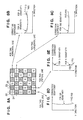
- Figs. 8A to 8E show an RGB Bayer filter matrix and shading correction coefficients corresponding to the matrix.
- Fig. 8A shows the RGB Bayer filter matrix
- Fig. 8B shows shading correction coefficients H1(i) and H2(i) corresponding to the first row of the RGB primary color Bayer filters
- Fig. 8C shows shading correction coefficients H1(i) and H2(i) corresponding to the second row of the RGB primary color Bayer filters
- Fig. 8D shows shading correction coefficients V1(j) and V2(j) corresponding to the first column of the RGB primary color Bayer filters
- Fig. 8E shows shading correction coefficients V1(j) and V2(j) corresponding to the second column of the RGB primary color Bayer filters.
- the RGB primary color Bayer filters have a matrix shown in Fig. 8A, G and R alternately appear in, e.g., the first horizontal line (first row), and the output sensitivity of a pixel (G) located at each odd-numbered position counted from the left end is different from that of a pixel (R) located at each even-numbered position. That is, the output of each pixel having an R filter is greatly lower than that of a pixel having a G filter at the peripheral portion. For this reason, the shading correction coefficients H1(i) and H2(i) shown in Fig. 8B are set.
- the shading correction coefficients H1(i) are applied to the outputs from the pixels having the R filter, and are stored in the H memory (H1) 12 in Fig. 1.
- the correction coefficients H2(i) are applied to the outputs from the pixels having the G filter, and are stored in the H memory (H2) 13 in Fig. 1.
- the output sensitivity of a pixel (G) located at each odd-numbered position counted from the upper end is nearly the same as that of a pixel (B) located at each even-numbered position.
- identical shading correction coefficients V1(j) and V2(j) shown in Fig. 8D are set.
- the shading correction coefficients V1(j) are applied to the outputs from the pixels having a G filter, and are stored in the V memory (V1) 14 in Fig. 1.
- the shading correction coefficients V2(j) are applied to the outputs from the pixels having a B filter, and are stored in the V memory (V2) 15 in Fig. 1.
- the shading correction coefficients V1(j) and V2(j) shown in Fig. 8E are set.
- the shading correction coefficients V1(j) are applied to the outputs from the pixels having the R filter, and are stored in the V memory (V1) 14 in Fig. 1.
- the correction coefficients V2(j) are applied to the outputs from the pixels having the G filter, and are stored in the V memory (V2) 15 in Fig. 1.
- the shading correction coefficients are set and stored, and luminance data for each pixel from the image sensing element 5 is multiplied by the corresponding shading correction coefficient read out based on two-dimensional addresses of the position of the pixel of interest. This process will be described below with reference to Fig. 9.
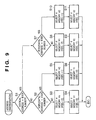
- Fig. 9 is a flow chart showing the sequence of an output process of the predetermined signals HSEL and VSEL executed by the address discrimination circuit 11.
- step S1 It is checked in step S1 if an address in the vertical (column) direction of the RGB primary color Bayer filters of the two-dimensional addresses of a pixel of interest sent from the address generation circuit 10 is an even number. Also, it is checked in steps S2 and S7 if an address in the horizontal (row) direction of the RGB primary color Bayer filters of the two-dimensional addresses of the pixel of interest sent from the address generation circuit 10 is an even number.
- the flow advances to step S3, and the address discrimination circuit 11 sets the predetermined signal HSEL at L level (0 level).
- the selector 16 sends the shading correction coefficients H1(i) as the outputs from the H memory (H1) 12 to the multiplier circuit (MUL1) 18.
- step S4 the address discrimination circuit 11 sets the predetermined signal VSEL at L level (0 level).
- the selector 17 sends the shading correction coefficients V1(j) as the output from the V memory (V1) 14 to the multiplier circuit (MUL2) 19.
- the multiplier circuit (MUL1) 18 makes multiplication correction for output data of pixels using the shading correction coefficients H1(i) (the left side of the H direction corresponds to a lower address in the horizontal direction, and the right side of the H direction corresponds to an upper address in the horizontal direction) indicated by the solid curve in Fig. 8B.
- the multiplier circuit (MUL2) 19 makes multiplication correction for output data of pixels using the characteristics of the shading correction coefficients V1(j) (the upper side of the V direction corresponds to a lower address in the vertical direction, and the lower side of the V direction corresponds to an upper address in the vertical direction) indicated by the solid curve in Fig. 8D.
- step S5 the address discrimination circuit 11 sets the predetermined signal HSEL at H level (1 level). Consequently, the selector 16 sends the shading correction coefficients H2(i) as the outputs from the H memory (H2) 13 to the multiplier circuit (MUL1) 18.
- step S6 the address discrimination circuit 11 sets the predetermined signal VSEL at L level (0 level).
- the selector 17 sends the shading correction coefficients V1(j) as the output from the V memory (V1) 14 to the multiplier circuit (MUL2) 19.
- the multiplier circuit (MUL1) 18 makes multiplication correction for output data of pixels using the shading correction coefficients H2(i) (the left side of the H direction corresponds to a lower address in the horizontal direction, and the right side of the H direction corresponds to an upper address in the horizontal direction) indicated by the broken curve in Fig. 8B.
- the multiplier circuit (MUL2) 19 makes multiplication correction for output data of pixels using the characteristics of the shading correction coefficients V1(j) (the upper side of the V direction corresponds to a lower address in the vertical direction, and the lower side of the V direction corresponds to an upper address in the vertical direction) indicated by the solid curve in Fig. 8E.
- the flow advances to step S8, and the address discrimination circuit 11 sets the predetermined signal HSEL at L level (0 level).
- the selector 16 sends the shading correction coefficients H1(i) as the outputs from the H memory (H1) 12 to the multiplier circuit (MUL1) 18.
- step S9 the address discrimination circuit 11 sets the predetermined signal VSEL at H level (1 level).
- the selector 17 sends the shading correction coefficients V2(j) as the output from the V memory (V2) 15 to the multiplier circuit (MUL2) 19.
- the multiplier circuit (MUL1) 18 makes multiplication correction for output data of pixels using the shading correction coefficients H1(i) (the left side of the H direction corresponds to a lower address in the horizontal direction, and the right side of the H direction corresponds to an upper address in the horizontal direction) indicated by the solid curve in Fig. 8C.
- the multiplier circuit (MUL2) 19 makes multiplication correction for output data of pixels using the characteristics of the shading correction coefficients V2(j) (the upper side of the V direction corresponds to a lower address in the vertical direction, and the lower side of the V direction corresponds to an upper address in the vertical direction) indicated by the solid curve in Fig. 8D.
- the flow advances to step S10, and the address discrimination circuit 11 sets the predetermined signal HSEL at H level (1 level). Consequently, the selector 16 sends the shading correction coefficients H2(i) as the outputs from the H memory (H2) 13 to the multiplier circuit (MUL1) 18.
- step S11 the address discrimination circuit 11 sets the predetermined signal VSEL at H level (1 level). Hence, the selector 17 sends the shading correction coefficients V2(j) as the output from the V memory (V2) 15 to the multiplier circuit (MUL2) 19.
- the multiplier circuit (MUL1) 18 makes multiplication correction for output data of pixels using the shading correction coefficients H2(i) (the left side of the H direction corresponds to a lower address in the horizontal direction, and the right side of the H direction corresponds to an upper address in the horizontal direction) indicated by the solid curve in Fig. 8C.
- the multiplier circuit (MUL2) 19 makes multiplication correction for output data of pixels using the characteristics of the shading correction coefficients V2(j) (the upper side of the V direction corresponds to a lower address in the vertical direction, and the lower side of the V direction corresponds to an upper address in the vertical direction) indicated by the broken curve in Fig. 8E.
- the address discrimination circuit 11 discriminates the two-dimensional addresses of the pixel of interest, and switches the shading correction coefficient tables by checking if the horizontal and vertical addresses are odd or even numbers.
- color shading produced due to an optical combination of the exchangeable lens 3 and infrared cut filters 4 shown in Fig. 12C can be prevented.
- red shading is prevented.
- the present invention is not limited to red, but can be applied to color shading of other colors.
- two different shading correction coefficients are prepared respectively in the horizontal and vertical directions.
- different shading correction coefficients may be prepared in correspondence with R, G, and B.
- four different types of shading correction coefficients may be prepared in each direction.
- the objects of the present invention can also be achieved by supplying a storage medium, which records a program code of a software program that can implement the functions of the above-mentioned embodiment to a system or apparatus, and reading out and executing the program code stored in the storage medium by a computer (or a CPU or MPU) of the system or apparatus.
- the program code itself read out from the storage medium implements the functions of the above-mentioned embodiments, and the storage medium which stores the program code constitutes the present invention.
- the storage medium for supplying the program code for example, a floppy disk, hard disk, optical disk, magneto-optical disk, CD-ROM, CD-R, magnetic tape, nonvolatile memory card, ROM, and the like may be used.
- the functions of the above-mentioned embodiments may be implemented not only by executing the readout program code by the computer but also by some or all of actual processing operations executed by an OS (operating system) running on the computer on the basis of an instruction of the program code.
- OS operating system
- the functions of the above-mentioned embodiments may be implemented by some or all of actual processing operations executed by a CPU or the like arranged in a function extension board or a function extension unit, which is inserted in or connected to the computer, after the program code read out from the storage medium is written in a memory of the extension board or unit.
- the shading correction precision can be improved.
- color shading produced in only a specific channel can be adequately corrected even when the lens is exchanged.
Landscapes
- Engineering & Computer Science (AREA)
- Multimedia (AREA)
- Signal Processing (AREA)
- Color Television Image Signal Generators (AREA)
- Studio Devices (AREA)
- Transforming Light Signals Into Electric Signals (AREA)
- Facsimile Image Signal Circuits (AREA)
Abstract
Description
Claims (18)
- An image sensing apparatus which comprises an image sensing element and means for exchangeably mounting a lens, characterized by comprising:storage means for storing shading correction coefficients respectively corresponding to pixels of the image sensing element; andcorrection means for making a correction calculation of pixel data read out from each pixel of the image sensing element by extracting the shading correction coefficient associated with the corresponding pixel from the shading correction coefficients stored in said storage means, andin that said storage means independently stores the shading correction coefficients in correspondence with pixels which are influenced by a color filter, which does not transmit a specific wavelength range and is inserted between the lens and the image sensing element, and pixels which are not influenced by the color filter.
- The apparatus according to claim 1, characterized by further comprising:extraction means for extracting exit pupil position information stored in the lens; andcalculation means for calculating shading correction coefficients on the basis of the exit pupil position information extracted by said extraction means, and sending the shading correction coefficients to said storage means.
- The apparatus according to claim 2, characterized in that said calculation means calculates the shading correction coefficients on the basis of the exit pupil position information extracted by said extraction means, and an image height of a corresponding pixel.
- The apparatus according to claim 3, characterized by further comprising:correction means for correcting the exit pupil position information extracted by said extraction means in accordance with at least one of a zoom position, focus position, image height, and aperture value of the lens, and sending the corrected exit pupil position information to said calculation means.
- The apparatus according to claim 3 or 4, characterized in that the exit pupil position information is information that represents a distance between the lens and the image sensing element on an optical axis.
- The apparatus according to any one of claims 3 to 5, characterized in that the image height is a distance between a position of a pixel of interest and a point on an optical axis on the plane of the image sensing element.
- The apparatus according to any one of claims 1 to 6, characterized in that said storage means stores the shading correction coefficients while classifying the shading correction coefficients into components in two orthogonal directions on the plane of the image sensing element.
- The apparatus according to claim 7, characterized in that said correction means multiplies the pixel data by the shading correction coefficient to correct the pixel data.
- The apparatus according to claim 8, characterized in that said correction means extracts two shading correction coefficients from the shading correction coefficients stored in said storage means in accordance with addresses of the corresponding pixel in the two directions, and multiplies the pixel data read out from the corresponding pixel by the two extracted shading correction coefficients in turn to correct the pixel data.
- A shading correction method applied to an image sensing apparatus,
element which can mount exchangeable lenses, characterised by comprising:the correction step of making a correction calculation of pixel data read out from each pixel of the image sensing element by extracting the shading correction coefficient associated with the corresponding pixel from shading correction coefficients stored in storage means which stores shading correction coefficients respectively corresponding to pixels of the image sensing element, andin that the shading correction coefficients are independently stored in said storage means in correspondence with pixels which are influenced by a color filter, which does not transmit a specific wavelength range and is inserted between the lens and the image sensing element, and pixels which are not influenced by the color filter. - The method according to claim 10, characterized by further comprising:the extraction step of extracting exit pupil position information stored in the lens; andthe calculation step of calculating shading correction coefficients on the basis of the exit pupil position information extracted in the extraction step, and sending the shading correction coefficients to said storage means.
- The method according to claim 11, characterized in that the calculation step includes the step of calculating the shading correction coefficients on the basis of the exit pupil position information extracted in the extraction step, and an image height of a corresponding pixel.
- The method according to claim 12, characterized by further comprising:the correction step of correcting the exit pupil position information extracted in the extraction step in accordance with at least one of a zoom position, focus position, image height, and aperture value of the lens, and supplying the corrected exit pupil position information to the calculation in the calculation step.
- The method according to any one of claims 10 to 13, characterized in that the storage step includes the step of storing in said storage means the shading correction coefficients while classifying the shading correction coefficients into components in two orthogonal directions on the plane of the image sensing element.
- The method according to claim 14, characterized in that the correction step includes the step of multiplying the pixel data by the shading correction coefficient to correct the pixel data.
- The method according to claim 15, characterized in that the correction step includes the step of extracting two shading correction coefficients from the shading correction coefficients stored in said storage means in accordance with addresses of the corresponding pixel in the two directions, and multiplying the pixel data read out from the corresponding pixel by the two extracted shading correction coefficients in turn to correct the pixel data.
- A program for making a computer implement a shading correction method cited in any one of claims 10 to 16.
- A storage medium characterized by computer-readably storing a program cited in claim 17.
Applications Claiming Priority (2)
| Application Number | Priority Date | Filing Date | Title |
|---|---|---|---|
| JP2001009474 | 2001-01-17 | ||
| JP2001009474A JP4574022B2 (en) | 2001-01-17 | 2001-01-17 | Imaging apparatus and shading correction method |
Publications (3)
| Publication Number | Publication Date |
|---|---|
| EP1227669A2 true EP1227669A2 (en) | 2002-07-31 |
| EP1227669A3 EP1227669A3 (en) | 2008-06-04 |
| EP1227669B1 EP1227669B1 (en) | 2011-12-07 |
Family
ID=18876955
Family Applications (1)
| Application Number | Title | Priority Date | Filing Date |
|---|---|---|---|
| EP02250153A Expired - Lifetime EP1227669B1 (en) | 2001-01-17 | 2002-01-10 | Image sensing apparatus, shading correction method, program, and storage medium |
Country Status (4)
| Country | Link |
|---|---|
| US (1) | US6937777B2 (en) |
| EP (1) | EP1227669B1 (en) |
| JP (1) | JP4574022B2 (en) |
| CN (1) | CN1226864C (en) |
Cited By (5)
| Publication number | Priority date | Publication date | Assignee | Title |
|---|---|---|---|---|
| EP1814079A1 (en) * | 2006-01-25 | 2007-08-01 | Sick Ag | Method and device for correcting the brightness of a raw image produced using a sensor matrix |
| EP2833621A1 (en) * | 2013-08-01 | 2015-02-04 | Harvest Imaging bvba | Image sensor with shading detection |
| US9503698B2 (en) | 2013-08-01 | 2016-11-22 | Harvest Imaging bvba | Image sensor with shading detection |
| EP3531683A1 (en) * | 2018-02-23 | 2019-08-28 | Omron Corporation | Image sensor |
| EP3531692A1 (en) * | 2018-02-23 | 2019-08-28 | Omron Corporation | Image sensor |
Families Citing this family (53)
| Publication number | Priority date | Publication date | Assignee | Title |
|---|---|---|---|---|
| JP4034614B2 (en) * | 2002-08-06 | 2008-01-16 | 富士フイルム株式会社 | Solid-state imaging device |
| US7388610B2 (en) | 2002-08-16 | 2008-06-17 | Zoran Corporation | Techniques of modifying image field data by extrapolation |
| US7391450B2 (en) | 2002-08-16 | 2008-06-24 | Zoran Corporation | Techniques for modifying image field data |
| US7408576B2 (en) * | 2002-08-16 | 2008-08-05 | Zoran Corporation | Techniques for modifying image field data as a function of radius across the image field |
| JP4115220B2 (en) * | 2002-09-19 | 2008-07-09 | キヤノン株式会社 | Imaging device |
| JP3981034B2 (en) | 2003-03-25 | 2007-09-26 | 富士フイルム株式会社 | Color image acquisition device and color electronic camera |
| JP4377622B2 (en) * | 2003-07-16 | 2009-12-02 | オリンパス株式会社 | Shading correction device |
| JP3824237B2 (en) * | 2003-09-05 | 2006-09-20 | ソニー株式会社 | Image processing apparatus and method, recording medium, and program |
| CN1820496B (en) * | 2003-10-31 | 2011-08-03 | 三菱电机株式会社 | Image Correction Method and Camera Device |
| JP4283704B2 (en) * | 2004-02-25 | 2009-06-24 | 富士フイルム株式会社 | Imaging device |
| JP2005341033A (en) * | 2004-05-25 | 2005-12-08 | Konica Minolta Photo Imaging Inc | Imaging apparatus and program |
| JP4703206B2 (en) * | 2004-05-31 | 2011-06-15 | 東芝モバイルディスプレイ株式会社 | Display device with image capture function |
| KR100615277B1 (en) * | 2004-08-18 | 2006-08-25 | 엠텍비젼 주식회사 | Method and device for correcting lens shading phenomenon in image sensor |
| JP2006121612A (en) * | 2004-10-25 | 2006-05-11 | Konica Minolta Photo Imaging Inc | Imaging device |
| KR20060055940A (en) * | 2004-11-19 | 2006-05-24 | 삼성전자주식회사 | CDC including memory, image input device and image input method including same |
| JP4229053B2 (en) * | 2004-12-06 | 2009-02-25 | ソニー株式会社 | IMAGING DEVICE, IMAGING METHOD, AND PROGRAM FOR IMAGING PROCESS |
| KR100645634B1 (en) | 2004-12-16 | 2006-11-15 | 삼성전기주식회사 | Automatic lens shading correction method and device |
| JP4018705B2 (en) * | 2005-04-18 | 2007-12-05 | キヤノン株式会社 | Shading correction apparatus, correction method, and imaging apparatus |
| JP2007094742A (en) * | 2005-09-28 | 2007-04-12 | Olympus Corp | Image signal processing apparatus and image signal processing program |
| JP4946059B2 (en) * | 2006-01-11 | 2012-06-06 | 株式会社ニコン | Imaging device |
| JP5040662B2 (en) * | 2006-02-03 | 2012-10-03 | 株式会社ニコン | Image processing apparatus, image processing method, and image processing program |
| JP4476955B2 (en) * | 2006-03-17 | 2010-06-09 | 富士通マイクロエレクトロニクス株式会社 | Shading correction circuit and control method thereof |
| GB2442050A (en) * | 2006-08-29 | 2008-03-26 | Micron Technology Inc | Image pixel value correction |
| US7782380B2 (en) * | 2006-09-01 | 2010-08-24 | Aptina Imaging Corporation | Positional gain adjustment and surface generation for image processing |
| JP4871153B2 (en) * | 2007-01-29 | 2012-02-08 | パナソニック株式会社 | Separate head camera and camera head |
| US8078001B2 (en) * | 2007-05-11 | 2011-12-13 | Micron Technology, Inc. | Methods, apparatuses and systems for piecewise generation of pixel correction values for image processing |
| US20080278613A1 (en) * | 2007-05-11 | 2008-11-13 | Micron Technology, Inc. | Methods, apparatuses and systems providing pixel value adjustment for images produced with varying focal length lenses |
| JP4998092B2 (en) * | 2007-05-31 | 2012-08-15 | 富士通セミコンダクター株式会社 | Solid-state imaging circuit and camera system |
| US8463068B2 (en) | 2007-08-09 | 2013-06-11 | Micron Technology, Inc. | Methods, systems and apparatuses for pixel value correction using multiple vertical and/or horizontal correction curves |
| JP2009049609A (en) | 2007-08-16 | 2009-03-05 | Fujitsu Microelectronics Ltd | Correction circuit, correction method, and imaging apparatus |
| US8331722B2 (en) * | 2008-01-08 | 2012-12-11 | Aptina Imaging Corporation | Methods, apparatuses and systems providing pixel value adjustment for images produced by a camera having multiple optical states |
| GB0801443D0 (en) * | 2008-01-25 | 2008-03-05 | Micron Technology Inc | Methods, systems and apparatuses for pixel signal correction using elliptical hyperbolic cosines |
| JP5163319B2 (en) * | 2008-06-30 | 2013-03-13 | ソニー株式会社 | Image signal correction apparatus, imaging apparatus, image signal correction method, and program |
| JP2010103642A (en) * | 2008-10-21 | 2010-05-06 | Toshiba Corp | Shading correction device |
| JP5376993B2 (en) * | 2009-02-19 | 2013-12-25 | キヤノン株式会社 | Information processing apparatus, imaging apparatus, and information processing apparatus control method |
| JP4402161B1 (en) * | 2009-03-30 | 2010-01-20 | マスレ ホールディングス エルエルピー | Imaging apparatus, image reproducing apparatus, and imaging method |
| JP5475393B2 (en) | 2009-10-20 | 2014-04-16 | キヤノン株式会社 | Imaging system and correction method |
| US8218041B2 (en) * | 2010-02-01 | 2012-07-10 | Digital Imaging Systems Gmbh | Aperture shading correction |
| JP2011223562A (en) * | 2010-03-23 | 2011-11-04 | Fujifilm Corp | Imaging apparatus |
| US8520059B2 (en) * | 2010-03-24 | 2013-08-27 | Fujifilm Corporation | Stereoscopic image taking apparatus |
| JP2012018277A (en) | 2010-07-07 | 2012-01-26 | Olympus Imaging Corp | Imaging apparatus having optical path reflection type zoom lens |
| WO2012036019A1 (en) * | 2010-09-13 | 2012-03-22 | 富士フイルム株式会社 | Monocular 3d-imaging device, shading correction method for monocular 3d-imaging device, and program for monocular 3d-imaging device |
| JP2012222465A (en) * | 2011-04-05 | 2012-11-12 | Sony Corp | Image processing apparatus, image processing method, and computer program |
| WO2013099613A1 (en) * | 2011-12-28 | 2013-07-04 | 富士フイルム株式会社 | Imaging device, image correction method, interchangeable lens, and imaging device body |
| JP5914192B2 (en) | 2012-06-11 | 2016-05-11 | キヤノン株式会社 | Imaging apparatus and control method thereof |
| JP5620522B2 (en) * | 2013-01-07 | 2014-11-05 | オリンパスイメージング株式会社 | Imaging apparatus and imaging method |
| CN105580349B (en) * | 2013-09-27 | 2018-08-14 | 富士胶片株式会社 | Image processing apparatus, photographic device and image processing method |
| JP6614057B2 (en) * | 2016-07-21 | 2019-12-04 | リコーイメージング株式会社 | Focus detection apparatus, focus detection method, and photographing apparatus |
| JP6819630B2 (en) * | 2018-02-23 | 2021-01-27 | オムロン株式会社 | Image sensor and main unit module |
| US10667693B1 (en) * | 2018-11-16 | 2020-06-02 | Perkinelmer Health Sciences, Inc. | Systems, methods, and apparatus for interference filter correction based on angle of incidence |
| JP7267723B2 (en) | 2018-12-14 | 2023-05-02 | キヤノン株式会社 | Lens device, imaging device, processing device, and camera device |
| JP2021051038A (en) * | 2019-09-26 | 2021-04-01 | キヤノン株式会社 | Aberration estimation method, aberration estimation device, program, and recording medium |
| CN111311724B (en) * | 2020-01-20 | 2022-08-09 | 稿定(厦门)科技有限公司 | Shadow adding method, medium, device and apparatus for 3D characters |
Family Cites Families (26)
| Publication number | Priority date | Publication date | Assignee | Title |
|---|---|---|---|---|
| US5850575A (en) * | 1935-09-14 | 1998-12-15 | Nikon Corporation | Image vibration reduction device |
| JPH02123879A (en) * | 1988-11-01 | 1990-05-11 | Canon Inc | Interchangeable lens unit and imaging device |
| JPH0323415A (en) * | 1989-06-20 | 1991-01-31 | Canon Inc | Optical low-pass filter |
| JP2893983B2 (en) * | 1991-03-28 | 1999-05-24 | ソニー株式会社 | Imaging device |
| JP3336436B2 (en) * | 1991-04-02 | 2002-10-21 | 株式会社ニコン | Lithography system, information collecting apparatus, exposure apparatus, and semiconductor device manufacturing method |
| US5990941A (en) * | 1991-05-13 | 1999-11-23 | Interactive Pictures Corporation | Method and apparatus for the interactive display of any portion of a spherical image |
| JPH0530415A (en) * | 1991-07-24 | 1993-02-05 | Matsushita Electric Ind Co Ltd | White shading correction processor |
| US5420630A (en) * | 1992-09-11 | 1995-05-30 | Canon Kabushiki Kaisha | Image pickup apparatus performing white balance control based on data from regions of a frame |
| JPH06178198A (en) * | 1992-12-04 | 1994-06-24 | Nec Corp | Solid state image pickup device |
| JPH06197266A (en) * | 1992-12-24 | 1994-07-15 | Sony Corp | Lens and image pickup device |
| DE69422803T2 (en) * | 1993-03-03 | 2000-06-15 | Graham Stewart B. Street | Image orientation and device |
| US5365058A (en) * | 1993-06-16 | 1994-11-15 | Welch Allyn, Inc. | Compensating optical system for video monitor |
| DE69434685T2 (en) * | 1993-08-04 | 2006-09-14 | Canon K.K. | Image processing method and apparatus |
| KR100203239B1 (en) | 1995-02-16 | 1999-06-15 | 윤종용 | White Shading Correction Method and Device |
| JPH09211651A (en) * | 1996-01-31 | 1997-08-15 | Minolta Co Ltd | Lens interchangeable camera |
| JPH09307789A (en) * | 1996-05-17 | 1997-11-28 | Olympus Optical Co Ltd | Image processing unit |
| JPH09318993A (en) * | 1996-05-30 | 1997-12-12 | Canon Inc | Solid-state image sensor camera system, interchangeable lens for photography, and optical accessories |
| US6088537A (en) * | 1997-04-15 | 2000-07-11 | Canon Kabushiki Kaisha | Focus detecting device |
| JPH11122525A (en) * | 1997-08-06 | 1999-04-30 | Minolta Co Ltd | Digital camera |
| JPH11164194A (en) * | 1997-11-28 | 1999-06-18 | Konica Corp | Image processing method and image input device |
| JP2000196953A (en) * | 1998-12-25 | 2000-07-14 | Olympus Optical Co Ltd | Camera system |
| JP3733771B2 (en) * | 1999-02-16 | 2006-01-11 | コニカミノルタホールディングス株式会社 | Imaging apparatus and shading correction method |
| JP3710947B2 (en) * | 1999-02-22 | 2005-10-26 | 株式会社小糸製作所 | VEHICLE LIGHT LENS MANUFACTURING METHOD AND VEHICLE LIGHT LENS MANUFACTURING DEVICE |
| JP4265029B2 (en) * | 1999-05-11 | 2009-05-20 | 株式会社ニコン | Image capturing device and interchangeable lens |
| JP3854754B2 (en) * | 1999-06-30 | 2006-12-06 | キヤノン株式会社 | Imaging apparatus, image processing apparatus and method, and memory medium |
| DE10124474A1 (en) * | 2001-05-19 | 2002-11-21 | Zeiss Carl | Microlithographic exposure involves compensating path difference by controlled variation of first and/or second optical paths; image plane difference is essentially independent of incident angle |
-
2001
- 2001-01-17 JP JP2001009474A patent/JP4574022B2/en not_active Expired - Fee Related
-
2002
- 2002-01-10 EP EP02250153A patent/EP1227669B1/en not_active Expired - Lifetime
- 2002-01-15 US US10/053,189 patent/US6937777B2/en not_active Expired - Fee Related
- 2002-01-17 CN CNB021020280A patent/CN1226864C/en not_active Expired - Fee Related
Cited By (10)
| Publication number | Priority date | Publication date | Assignee | Title |
|---|---|---|---|---|
| EP1814079A1 (en) * | 2006-01-25 | 2007-08-01 | Sick Ag | Method and device for correcting the brightness of a raw image produced using a sensor matrix |
| US7714914B2 (en) | 2006-01-25 | 2010-05-11 | Sick Ag | Method and device for the correction of the brightness of a raw image generated by a sensor matrix |
| EP2833621A1 (en) * | 2013-08-01 | 2015-02-04 | Harvest Imaging bvba | Image sensor with shading detection |
| US9503698B2 (en) | 2013-08-01 | 2016-11-22 | Harvest Imaging bvba | Image sensor with shading detection |
| EP3531683A1 (en) * | 2018-02-23 | 2019-08-28 | Omron Corporation | Image sensor |
| EP3531692A1 (en) * | 2018-02-23 | 2019-08-28 | Omron Corporation | Image sensor |
| CN110191277A (en) * | 2018-02-23 | 2019-08-30 | 欧姆龙株式会社 | Imaging sensor |
| US10863107B2 (en) | 2018-02-23 | 2020-12-08 | Omron Corporation | Image sensor configured by imaging module installed in body module and lens module, and capable of performing good shading correction |
| US11019278B2 (en) | 2018-02-23 | 2021-05-25 | Omron Corporation | Image sensor configured by an imaging module installed in a body module and a lens module, and is capable of performing good shading correction |
| CN110191277B (en) * | 2018-02-23 | 2022-04-05 | 欧姆龙株式会社 | Image Sensor |
Also Published As
| Publication number | Publication date |
|---|---|
| CN1366423A (en) | 2002-08-28 |
| JP4574022B2 (en) | 2010-11-04 |
| US20020094131A1 (en) | 2002-07-18 |
| EP1227669B1 (en) | 2011-12-07 |
| EP1227669A3 (en) | 2008-06-04 |
| US6937777B2 (en) | 2005-08-30 |
| CN1226864C (en) | 2005-11-09 |
| JP2002218298A (en) | 2002-08-02 |
Similar Documents
| Publication | Publication Date | Title |
|---|---|---|
| US6937777B2 (en) | Image sensing apparatus, shading correction method, program, and storage medium | |
| US12294795B2 (en) | Image sensor and image-capturing device | |
| US8063978B2 (en) | Image pickup device, focus detection device, image pickup apparatus, method for manufacturing image pickup device, method for manufacturing focus detection device, and method for manufacturing image pickup apparatus | |
| US10389959B2 (en) | Image-capturing device and image sensor | |
| US7715703B2 (en) | Image sensor and image capturing device | |
| US6750437B2 (en) | Image pickup apparatus that suitably adjusts a focus | |
| EP1458183A2 (en) | Camera using a beam splitter with micro-lens array for image amplification | |
| US20140340565A1 (en) | Image capturing apparatus and control method thereof | |
| EP2212731B1 (en) | Image sensing apparatus | |
| US8902349B2 (en) | Image pickup apparatus | |
| JP2003032694A (en) | Solid-state image sensor and digital camera | |
| JP5680797B2 (en) | Imaging apparatus, image processing apparatus, and image processing method | |
| US11290648B2 (en) | Image capture apparatus and control method thereof | |
| US6831687B1 (en) | Digital camera and image signal processing apparatus | |
| CN104641276B (en) | Camera head and signal processing method | |
| EP1067777A2 (en) | Image sensing device, image processing apparatus and method, and memory medium | |
| US20160044231A1 (en) | Image capturing apparatus and method of controlling the same | |
| US8144217B2 (en) | Image sensing apparatus | |
| EP1484928B1 (en) | Imaging device | |
| US11025884B2 (en) | Image capturing apparatus, control method thereof, and storage medium | |
| JP2018163322A (en) | Imaging device and method for controlling the same, program, and recording medium | |
| JP7157642B2 (en) | IMAGING DEVICE, CONTROL METHOD, AND PROGRAM | |
| JP6711886B2 (en) | Imaging device, control method thereof, program, and storage medium | |
| JP2001069516A (en) | Color imaging apparatus and digital still camera using the same | |
| JP2008312087A (en) | Imaging device |
Legal Events
| Date | Code | Title | Description |
|---|---|---|---|
| PUAI | Public reference made under article 153(3) epc to a published international application that has entered the european phase |
Free format text: ORIGINAL CODE: 0009012 |
|
| AK | Designated contracting states |
Kind code of ref document: A2 Designated state(s): AT BE CH CY DE DK ES FI FR GB GR IE IT LI LU MC NL PT SE TR |
|
| AX | Request for extension of the european patent |
Free format text: AL;LT;LV;MK;RO;SI |
|
| PUAL | Search report despatched |
Free format text: ORIGINAL CODE: 0009013 |
|
| AK | Designated contracting states |
Kind code of ref document: A3 Designated state(s): AT BE CH CY DE DK ES FI FR GB GR IE IT LI LU MC NL PT SE TR |
|
| AX | Request for extension of the european patent |
Extension state: AL LT LV MK RO SI |
|
| 17P | Request for examination filed |
Effective date: 20081204 |
|
| AKX | Designation fees paid |
Designated state(s): DE FR GB |
|
| 17Q | First examination report despatched |
Effective date: 20090224 |
|
| GRAP | Despatch of communication of intention to grant a patent |
Free format text: ORIGINAL CODE: EPIDOSNIGR1 |
|
| GRAS | Grant fee paid |
Free format text: ORIGINAL CODE: EPIDOSNIGR3 |
|
| GRAA | (expected) grant |
Free format text: ORIGINAL CODE: 0009210 |
|
| AK | Designated contracting states |
Kind code of ref document: B1 Designated state(s): DE FR GB |
|
| REG | Reference to a national code |
Ref country code: GB Ref legal event code: FG4D |
|
| REG | Reference to a national code |
Ref country code: DE Ref legal event code: R096 Ref document number: 60241696 Country of ref document: DE Effective date: 20120209 |
|
| PLBE | No opposition filed within time limit |
Free format text: ORIGINAL CODE: 0009261 |
|
| STAA | Information on the status of an ep patent application or granted ep patent |
Free format text: STATUS: NO OPPOSITION FILED WITHIN TIME LIMIT |
|
| 26N | No opposition filed |
Effective date: 20120910 |
|
| REG | Reference to a national code |
Ref country code: DE Ref legal event code: R097 Ref document number: 60241696 Country of ref document: DE Effective date: 20120910 |
|
| REG | Reference to a national code |
Ref country code: FR Ref legal event code: PLFP Year of fee payment: 14 |
|
| PGFP | Annual fee paid to national office [announced via postgrant information from national office to epo] |
Ref country code: DE Payment date: 20150131 Year of fee payment: 14 |
|
| PGFP | Annual fee paid to national office [announced via postgrant information from national office to epo] |
Ref country code: FR Payment date: 20150126 Year of fee payment: 14 Ref country code: GB Payment date: 20150123 Year of fee payment: 14 |
|
| REG | Reference to a national code |
Ref country code: DE Ref legal event code: R119 Ref document number: 60241696 Country of ref document: DE |
|
| GBPC | Gb: european patent ceased through non-payment of renewal fee |
Effective date: 20160110 |
|
| REG | Reference to a national code |
Ref country code: FR Ref legal event code: ST Effective date: 20160930 |
|
| PG25 | Lapsed in a contracting state [announced via postgrant information from national office to epo] |
Ref country code: GB Free format text: LAPSE BECAUSE OF NON-PAYMENT OF DUE FEES Effective date: 20160110 Ref country code: DE Free format text: LAPSE BECAUSE OF NON-PAYMENT OF DUE FEES Effective date: 20160802 |
|
| PG25 | Lapsed in a contracting state [announced via postgrant information from national office to epo] |
Ref country code: FR Free format text: LAPSE BECAUSE OF NON-PAYMENT OF DUE FEES Effective date: 20160201 |