EP1226946B1 - Two-step trench etch for a fully integrated thermal inkjet printhead - Google Patents
Two-step trench etch for a fully integrated thermal inkjet printhead Download PDFInfo
- Publication number
- EP1226946B1 EP1226946B1 EP02250340A EP02250340A EP1226946B1 EP 1226946 B1 EP1226946 B1 EP 1226946B1 EP 02250340 A EP02250340 A EP 02250340A EP 02250340 A EP02250340 A EP 02250340A EP 1226946 B1 EP1226946 B1 EP 1226946B1
- Authority
- EP
- European Patent Office
- Prior art keywords
- substrate
- ink feed
- protection layer
- thin film
- layer
- Prior art date
- Legal status (The legal status is an assumption and is not a legal conclusion. Google has not performed a legal analysis and makes no representation as to the accuracy of the status listed.)
- Expired - Lifetime
Links
- 238000000034 method Methods 0.000 claims description 49
- 239000000758 substrate Substances 0.000 claims description 49
- 239000010409 thin film Substances 0.000 claims description 49
- WGTYBPLFGIVFAS-UHFFFAOYSA-M tetramethylammonium hydroxide Chemical compound [OH-].C[N+](C)(C)C WGTYBPLFGIVFAS-UHFFFAOYSA-M 0.000 claims description 22
- 238000005530 etching Methods 0.000 claims description 17
- 238000004519 manufacturing process Methods 0.000 claims description 7
- 239000012528 membrane Substances 0.000 claims description 7
- 230000000873 masking effect Effects 0.000 claims description 6
- 150000004767 nitrides Chemical class 0.000 claims description 6
- 238000007639 printing Methods 0.000 claims description 6
- 238000000151 deposition Methods 0.000 claims description 5
- BOTDANWDWHJENH-UHFFFAOYSA-N Tetraethyl orthosilicate Chemical compound CCO[Si](OCC)(OCC)OCC BOTDANWDWHJENH-UHFFFAOYSA-N 0.000 claims description 4
- 239000000463 material Substances 0.000 claims description 4
- 239000010410 layer Substances 0.000 description 103
- 239000000976 ink Substances 0.000 description 92
- 239000005360 phosphosilicate glass Substances 0.000 description 10
- 230000008569 process Effects 0.000 description 9
- 235000012431 wafers Nutrition 0.000 description 9
- XUIMIQQOPSSXEZ-UHFFFAOYSA-N Silicon Chemical compound [Si] XUIMIQQOPSSXEZ-UHFFFAOYSA-N 0.000 description 8
- 239000004020 conductor Substances 0.000 description 8
- 229910052710 silicon Inorganic materials 0.000 description 8
- 239000010703 silicon Substances 0.000 description 8
- 238000007796 conventional method Methods 0.000 description 7
- 229910016570 AlCu Inorganic materials 0.000 description 4
- 239000010931 gold Substances 0.000 description 4
- 238000002161 passivation Methods 0.000 description 4
- 230000000712 assembly Effects 0.000 description 3
- 238000000429 assembly Methods 0.000 description 3
- PCHJSUWPFVWCPO-UHFFFAOYSA-N gold Chemical compound [Au] PCHJSUWPFVWCPO-UHFFFAOYSA-N 0.000 description 3
- 229910052737 gold Inorganic materials 0.000 description 3
- 238000001020 plasma etching Methods 0.000 description 3
- 239000011241 protective layer Substances 0.000 description 3
- ZOXJGFHDIHLPTG-UHFFFAOYSA-N Boron Chemical compound [B] ZOXJGFHDIHLPTG-UHFFFAOYSA-N 0.000 description 2
- 230000002411 adverse Effects 0.000 description 2
- 229910052796 boron Inorganic materials 0.000 description 2
- 230000000694 effects Effects 0.000 description 2
- 239000012530 fluid Substances 0.000 description 2
- 238000009413 insulation Methods 0.000 description 2
- 229910052715 tantalum Inorganic materials 0.000 description 2
- GUVRBAGPIYLISA-UHFFFAOYSA-N tantalum atom Chemical compound [Ta] GUVRBAGPIYLISA-UHFFFAOYSA-N 0.000 description 2
- 239000004593 Epoxy Substances 0.000 description 1
- PIICEJLVQHRZGT-UHFFFAOYSA-N Ethylenediamine Chemical compound NCCN PIICEJLVQHRZGT-UHFFFAOYSA-N 0.000 description 1
- KWYUFKZDYYNOTN-UHFFFAOYSA-M Potassium hydroxide Chemical compound [OH-].[K+] KWYUFKZDYYNOTN-UHFFFAOYSA-M 0.000 description 1
- 229910052581 Si3N4 Inorganic materials 0.000 description 1
- 229910004074 SiF6 Inorganic materials 0.000 description 1
- 230000009471 action Effects 0.000 description 1
- RVSGESPTHDDNTH-UHFFFAOYSA-N alumane;tantalum Chemical compound [AlH3].[Ta] RVSGESPTHDDNTH-UHFFFAOYSA-N 0.000 description 1
- 238000003491 array Methods 0.000 description 1
- 230000015572 biosynthetic process Effects 0.000 description 1
- 230000000903 blocking effect Effects 0.000 description 1
- 239000003086 colorant Substances 0.000 description 1
- 230000008021 deposition Effects 0.000 description 1
- 238000010292 electrical insulation Methods 0.000 description 1
- 238000005516 engineering process Methods 0.000 description 1
- 238000010304 firing Methods 0.000 description 1
- 230000007246 mechanism Effects 0.000 description 1
- 230000003287 optical effect Effects 0.000 description 1
- 239000002245 particle Substances 0.000 description 1
- 238000000206 photolithography Methods 0.000 description 1
- 230000005855 radiation Effects 0.000 description 1
- HBMJWWWQQXIZIP-UHFFFAOYSA-N silicon carbide Chemical compound [Si+]#[C-] HBMJWWWQQXIZIP-UHFFFAOYSA-N 0.000 description 1
- 229910010271 silicon carbide Inorganic materials 0.000 description 1
- HQVNEWCFYHHQES-UHFFFAOYSA-N silicon nitride Chemical compound N12[Si]34N5[Si]62N3[Si]51N64 HQVNEWCFYHHQES-UHFFFAOYSA-N 0.000 description 1
- IGELFKKMDLGCJO-UHFFFAOYSA-N xenon difluoride Chemical compound F[Xe]F IGELFKKMDLGCJO-UHFFFAOYSA-N 0.000 description 1
Images


Classifications
-
- B—PERFORMING OPERATIONS; TRANSPORTING
- B41—PRINTING; LINING MACHINES; TYPEWRITERS; STAMPS
- B41J—TYPEWRITERS; SELECTIVE PRINTING MECHANISMS, i.e. MECHANISMS PRINTING OTHERWISE THAN FROM A FORME; CORRECTION OF TYPOGRAPHICAL ERRORS
- B41J2/00—Typewriters or selective printing mechanisms characterised by the printing or marking process for which they are designed
- B41J2/005—Typewriters or selective printing mechanisms characterised by the printing or marking process for which they are designed characterised by bringing liquid or particles selectively into contact with a printing material
- B41J2/01—Ink jet
- B41J2/135—Nozzles
- B41J2/16—Production of nozzles
- B41J2/1601—Production of bubble jet print heads
- B41J2/1603—Production of bubble jet print heads of the front shooter type
-
- B—PERFORMING OPERATIONS; TRANSPORTING
- B41—PRINTING; LINING MACHINES; TYPEWRITERS; STAMPS
- B41J—TYPEWRITERS; SELECTIVE PRINTING MECHANISMS, i.e. MECHANISMS PRINTING OTHERWISE THAN FROM A FORME; CORRECTION OF TYPOGRAPHICAL ERRORS
- B41J2/00—Typewriters or selective printing mechanisms characterised by the printing or marking process for which they are designed
- B41J2/005—Typewriters or selective printing mechanisms characterised by the printing or marking process for which they are designed characterised by bringing liquid or particles selectively into contact with a printing material
- B41J2/01—Ink jet
- B41J2/135—Nozzles
- B41J2/14—Structure thereof only for on-demand ink jet heads
- B41J2/14016—Structure of bubble jet print heads
- B41J2/14088—Structure of heating means
- B41J2/14112—Resistive element
- B41J2/14129—Layer structure
-
- B—PERFORMING OPERATIONS; TRANSPORTING
- B41—PRINTING; LINING MACHINES; TYPEWRITERS; STAMPS
- B41J—TYPEWRITERS; SELECTIVE PRINTING MECHANISMS, i.e. MECHANISMS PRINTING OTHERWISE THAN FROM A FORME; CORRECTION OF TYPOGRAPHICAL ERRORS
- B41J2/00—Typewriters or selective printing mechanisms characterised by the printing or marking process for which they are designed
- B41J2/005—Typewriters or selective printing mechanisms characterised by the printing or marking process for which they are designed characterised by bringing liquid or particles selectively into contact with a printing material
- B41J2/01—Ink jet
- B41J2/135—Nozzles
- B41J2/16—Production of nozzles
- B41J2/1621—Manufacturing processes
- B41J2/1626—Manufacturing processes etching
- B41J2/1628—Manufacturing processes etching dry etching
-
- B—PERFORMING OPERATIONS; TRANSPORTING
- B41—PRINTING; LINING MACHINES; TYPEWRITERS; STAMPS
- B41J—TYPEWRITERS; SELECTIVE PRINTING MECHANISMS, i.e. MECHANISMS PRINTING OTHERWISE THAN FROM A FORME; CORRECTION OF TYPOGRAPHICAL ERRORS
- B41J2/00—Typewriters or selective printing mechanisms characterised by the printing or marking process for which they are designed
- B41J2/005—Typewriters or selective printing mechanisms characterised by the printing or marking process for which they are designed characterised by bringing liquid or particles selectively into contact with a printing material
- B41J2/01—Ink jet
- B41J2/135—Nozzles
- B41J2/16—Production of nozzles
- B41J2/1621—Manufacturing processes
- B41J2/1626—Manufacturing processes etching
- B41J2/1629—Manufacturing processes etching wet etching
-
- B—PERFORMING OPERATIONS; TRANSPORTING
- B41—PRINTING; LINING MACHINES; TYPEWRITERS; STAMPS
- B41J—TYPEWRITERS; SELECTIVE PRINTING MECHANISMS, i.e. MECHANISMS PRINTING OTHERWISE THAN FROM A FORME; CORRECTION OF TYPOGRAPHICAL ERRORS
- B41J2/00—Typewriters or selective printing mechanisms characterised by the printing or marking process for which they are designed
- B41J2/005—Typewriters or selective printing mechanisms characterised by the printing or marking process for which they are designed characterised by bringing liquid or particles selectively into contact with a printing material
- B41J2/01—Ink jet
- B41J2/135—Nozzles
- B41J2/16—Production of nozzles
- B41J2/1621—Manufacturing processes
- B41J2/1631—Manufacturing processes photolithography
-
- B—PERFORMING OPERATIONS; TRANSPORTING
- B41—PRINTING; LINING MACHINES; TYPEWRITERS; STAMPS
- B41J—TYPEWRITERS; SELECTIVE PRINTING MECHANISMS, i.e. MECHANISMS PRINTING OTHERWISE THAN FROM A FORME; CORRECTION OF TYPOGRAPHICAL ERRORS
- B41J2/00—Typewriters or selective printing mechanisms characterised by the printing or marking process for which they are designed
- B41J2/005—Typewriters or selective printing mechanisms characterised by the printing or marking process for which they are designed characterised by bringing liquid or particles selectively into contact with a printing material
- B41J2/01—Ink jet
- B41J2/135—Nozzles
- B41J2/16—Production of nozzles
- B41J2/1621—Manufacturing processes
- B41J2/1635—Manufacturing processes dividing the wafer into individual chips
-
- B—PERFORMING OPERATIONS; TRANSPORTING
- B41—PRINTING; LINING MACHINES; TYPEWRITERS; STAMPS
- B41J—TYPEWRITERS; SELECTIVE PRINTING MECHANISMS, i.e. MECHANISMS PRINTING OTHERWISE THAN FROM A FORME; CORRECTION OF TYPOGRAPHICAL ERRORS
- B41J2/00—Typewriters or selective printing mechanisms characterised by the printing or marking process for which they are designed
- B41J2/005—Typewriters or selective printing mechanisms characterised by the printing or marking process for which they are designed characterised by bringing liquid or particles selectively into contact with a printing material
- B41J2/01—Ink jet
- B41J2/135—Nozzles
- B41J2/16—Production of nozzles
- B41J2/1621—Manufacturing processes
- B41J2/164—Manufacturing processes thin film formation
- B41J2/1645—Manufacturing processes thin film formation thin film formation by spincoating
Definitions
- This invention relates to inkjet printers and, more particularly, to a monolithic printhead for an inkjet printer.
- Inkjet printers typically have a printhead mounted on a carriage that scans back and forth across the width of a sheet of paper feeding through the printer. Ink from an ink reservoir, either on-board the carriage or external to the carriage, is fed to ink ejection chambers on the printhead. Each ink ejection chamber contains an ink ejection element, such as a heater resistor or a piezoelectric element, which is independently addressable. Energizing an ink ejection element causes a droplet of ink to be ejected through a nozzle for creating a small dot on the medium. The pattern of dots created forms an image or text.
- an ink ejection element such as a heater resistor or a piezoelectric element
- a conventional method of etching a through-hole in a printhead substrate is known from US-A- 4 789 425.
- Described herein is a monolithic printhead formed using integrated circuit techniques. Thin film layers, including a resistive layer, are formed on a top surface of a silicon substrate. The various layers are etched to provide conductive leads to the heater resistor elements. Piezoelectric elements may be used instead of the resistive elements.
- At least one ink feed hole is formed through the thin film layers for each ink ejection chamber.
- a protective layer is deposited over the ink feed hole area.
- An orifice layer is formed on the top surface of the thin film layers to define the nozzles and ink ejection chambers.
- a photo-definable material is used to form the orifice layer.
- a trench mask is formed on the bottom surface of the substrate.
- a trench is etched (using, for example, TMAH) through the exposed bottom surface of the substrate.
- the trench completely etches away portions of the substrate beneath the ink feed holes.
- the protective layer prevents the TMAH from etching the substrate from the front side through the ink feed hole.
- the protective layer is then removed, and a second trench etch is performed.
- the TMAH solution etches away the substrate portion exposed through the ink feed holes.
- the second trench etch inherently aligns the edge of the trench with the ink feed holes. This two-step trench etch eases the tolerances for the trench mask and results in a precisely positioned trench, since the trench side walls are ultimately aligned to the thin film openings.
- a separate protection layer is not deposited. Instead, a field oxide (FOX) layer, formed over the substrate as one of the thin film layers, is used for protection.
- the ink feed holes are etched through the thin film layers down to the FOX layer.
- a first trench etch is conducted as in the previous embodiment.
- the portions of the FOX layer in the ink feed hole areas are removed with a buffered oxide etch.
- a second trench etch is then performed that self-aligns the trench sidewalls to the thin film openings. This process is more economical than the previous embodiment using a separate protection layer.
- the resulting fully integrated thermal inkjet printhead can be manufactured to a very precise tolerance since the entire structure is monolithic, meeting the needs for the next generation of printheads.
- the process may be used to form openings in devices other than printheads.
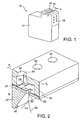
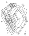
- FIG. 1 is a perspective view of one type of inkjet print cartridge 10 which may incorporate the printhead structures of the present invention.
- the print cartridge 10 of FIG. 1 is the type that contains a substantial quantity of ink within its body 12, but another suitable print cartridge may be the type that receives ink from an external ink supply either mounted on the printhead or connected to the printhead via a tube.
- the ink is supplied to a printhead 14.
- Printhead 14 to be described in detail later, channels the ink into ink ejection chambers, each chamber containing an ink ejection element. Electrical signals are provided to contacts 16 to individually energize the ink ejection elements to eject a droplet of ink through an associated nozzle 18.
- the structure and operation of conventional print cartridges are very well known.
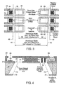
- FIG. 2 is a cross-sectional view of a portion of the printhead of FIG. 1 taken along line 2-2 in FIG. 1.
- a printhead may have 300 or more nozzles and associated ink ejection chambers, detail of only a single ink ejection chamber need be described in order to understand the invention. It should also be understood by those skilled in the art that many printheads are formed on a single silicon wafer and then separated from one another using conventional techniques.
- a silicon substrate 20 has formed on it various thin film layers 22, to be described in detail later.
- the thin film layers 22 include a resistive layer for forming resistors 24.
- Other thin film layers perform various functions, such as providing electrical insulation from the substrate 20, providing a thermally conductive path from the heater resistor elements to the substrate 20, and providing electrical conductors to the resistor elements.
- One electrical conductor 25 is shown leading to one end of a resistor 24.
- a similar conductor leads to the other end of the resistor 24.
- the resistors and conductors in a chamber would be obscured by overlying layers.
- Ink feed holes 26 are formed completely through the thin film layers 22. There may be multiple holes per chamber. Alternately, a manifold may be formed in the orifice layer 28 for providing a common ink channel for a row of ink ejection chambers 30
- An orifice layer 28 is deposited over the surface of the thin film layers 22 and etched to form ink ejection chambers 30, one chamber per resistor 24.
- Nozzles 34 may be formed using conventional photolithographic techniques.
- the silicon substrate 20 is etched to form a trench 36 extending along the length of the row of ink feed holes 26 so that ink 38 from an ink reservoir may enter the ink feed holes 26 for supplying ink to the ink ejection chambers 30.
- a two-step etch process is used to precisely align the edges of the trench 36 with the ink feed holes 26.
- each printhead is approximately one-half inch long and contains two offset rows of nozzles, each row containing 150 nozzles for a total of 300 nozzles per printhead.
- the printhead can thus print at a single pass resolution of 600 dots per inch (dpi) along the direction of the nozzle rows or print at a greater resolution in multiple passes. Greater resolutions may also be printed along the scan direction of the printhead. Resolutions of 1200 or greater dpi may be obtained using the present invention.
- an electrical signal is provided to heater resistor 24, which vaporizes a portion of the ink to form a bubble within the ink ejection chamber 30.
- the bubble propels an ink droplet through an associated nozzle 34 onto a medium.
- the ink ejection chamber is then refilled by capillary action.
- FIG. 3 is a top down view of the printhead of FIG. 2 showing two parallel arrays of ink ejection chambers formed in the printhead.
- the ink ejection chambers 30 in the two rows may be offset.
- Elements in the various figures designated with the same numerals may be similar or identical.
- the thin film layer shelf above the trench is referred to as a membrane.
- the width of this membrane is shown in FIG. 3 by the dashed lines 40.
- the particular method for forming the printhead of FIG. 2 uses a two-step trench etch process.
- the first trench etch results in a membrane width, shown by dash lines 42, that is narrower than the final membrane width 40. As will described below, this allows the mask for the first trench etch to have a very relaxed tolerance.
- the trench sidewalls after the second trench etch are self-aligned to the ink feed holes 26 defined by the thin film layers.
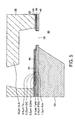
- FIG. 4 is a cross-sectional view along line 4-4 in FIG. 2, showing the additional portion of the printhead containing the second row of ink ejection chambers.
- the thin film layers 22, including the resistors 24, are shown simplified. Additional detail of FIG. 4 will be discussed with respect to FIGS. 5 and 6A-6G.
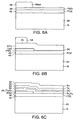
- FIG. 5 is a cross-sectional view along line 4-4 of FIG. 2 showing a single ink ejection chamber and the associated structure of the printhead.
- FIG. 5 shows one embodiment of the individual thin film layers
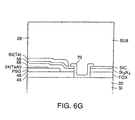
- FIGs. 6A-6G show various steps used to fabricate the printhead of FIGS. 2-5. Conventional deposition, masking, and etching steps are used unless otherwise noted.
- a silicon substrate 20 with a crystalline orientation of ⁇ 100> is placed in a vacuum chamber.
- the bulk silicon is about 675 microns thick.
- a field oxide layer 46 having a thickness of 1.2 microns, is formed over the silicon substrate 20 using conventional techniques.
- a phosphosilicate glass (PSG) layer 48 having a thickness of 0.5 microns, is then deposited over the field oxide layer 46 using conventional techniques.
- PSG phosphosilicate glass
- a mask 49 is formed over the PSG layer 48 using conventional photolithographic techniques.
- the mask 49 is also shown in FIGS. 3 and 7.
- the PSG layer 48 is then etched using conventional reactive ion etching (RIE) to pull back the PSG layer 48 from the subsequently formed ink feed hole. This will protect the PSG layer 48 from ink.
- RIE reactive ion etching
- a boron PSG or boron TEOS (BTEOS) layer may be used instead of PSG layer 48 and etched in a manner similar to the etching of layer 48.
- BTEOS boron TEOS
- TaAl tantalum aluminum
- Other known resistive layers can also be used.
- a conductive layer 25 of AlCu is then deposited over the TaAl.
- a mask 54 is deposited and patterned using conventional photolithographic techniques, and the conductive layer 25 and the resistive layer 50 are etched using conventional IC fabrication techniques.
- Another masking and etching step (not shown) is used to remove the portions of the AlCu over the heater resistors 24, as shown in FIG. 2. The resulting AlCu conductors are outside the field of view of FIGS. 6A-6G.
- the etching of the conductive layer 25 and resistive layer 50 define a first resistor dimension (e.g., a width).
- a second resistor dimension (e.g., a length) is defined by etching the conductive layer 25 to cause the resistive portion to be contacted by the conductive traces at two ends.
- This technique of forming resistors and electrical conductors is well known in the art.
- the conductive traces are formed so as to not extend across the middle of the printhead, but run along the edges. Appropriate addressing circuitry and pads are provided on the substrate 20 for providing energizing signals to the resistors 24.
- a silicon nitride layer 56 having a thickness of 0.5 microns. This layer provides insulation and passivation.
- nitride layer 56 Over the nitride layer 56 is formed a silicon carbide layer 58, having a thickness of 0.25 microns, to provide additional insulation and passivation.
- the nitride layer 56 and carbide layer 58 now protect the PSG layer 48 from the ink and etchant.
- Other dielectric layers may be used instead of nitride and carbide.
- passivation layers are then masked (outside the field of view) and etched using conventional techniques to expose portions of the conductive layer 25 for electrical contact to a subsequent gold conductive layer to provide ground lines.
- a bubble cavitation layer 60 of tantalum (Ta) is then formed over the carbide layer 58.
- Gold (Au) 62 is deposited over the tantalum layer 60 and etched to form the ground lines electrically connected to certain ones of the conductive layer 25 traces. The ground lines terminate in bond pads along edges of the substrate 20.
- the AlCu and gold conductors may be coupled to transistors formed on the substrate surface. Such transistors are described in U.S. Patent No. 5,648,806, previously mentioned.
- a mask 66 is patterned to expose a portion of the thin film layers to be etched to form the ink feed holes 26 (FIG. 2). Alternately, multiple masking and etching steps may be used as the various thin film layers are formed to etch the ink feed holes.
- the thin film layers are then etched using an anisotropic etch.
- This ink feed hole etch process can be a combination of several types of etches (RIE or wet).
- RIE etches
- the etch through the thin film layers may use conventional IC fabrication techniques.
- the resulting wafer after the etch is shown in FIG. 6E.
- the manufacturing process described below includes a technique to align the trench 36 with the ink feed holes 26.
- a frontside protection layer 70 is deposited and formed using conventional photolithographic techniques.
- the protection layer 70 is a plasma TEOS having a thickness (e.g., 1000 angstroms) that is thin enough so that it can be quickly and easily removed by a buffered oxide etch (BOE) but thick enough that it can withstand exposure to the TMAH (tetramethyl ammonium hydroxide) etchant throughout the approximately fifteen hour trench etch.
- the protection layer 70 may be any suitable material, including oxides, nitrides, and oxinitrides. A mask for this operation would be the inverse of the ink feed hole mask and biased slightly larger to ensure that the entire ink feed hole opening remains covered with a protection layer 70.
- FIG. 3 shows the protection layer 70 mask boundary.
- an orifice layer 28 is then deposited and formed.
- the orifice layer 28 may be formed of a spun-on epoxy called SU8. Orifice layer 28 may alternatively be laminated or screened on.
- the orifice layer in one embodiment is about 20 microns.
- the ink chambers 30 (FIG. 2) and nozzles 34 are formed through photolithography.
- a first mask using a half dosage of UV radiation "hardens" the upper surface of the SU8 except in locations where the nozzles 34 are to be formed.
- a second mask using a full UV dosage then exposes the SU8 in those areas where neither nozzles 34 nor ink ejection chambers 30 are to be formed. After these two exposures, the SU8 is developed, and the hardened portions remain but the nozzle portions and the ink ejection chamber portions of the SU8 are removed.
- the thin film layers and formed orifice layer 28 are shown in FIG. 4.
- the backside of the wafer is then masked (by mask 76) using conventional techniques to expose the portion of the backside of the wafer to be subjected to the TMAH trench etch.
- the backside mask 76 may be a FOX hardmask formed using conventional photolithographic techniques.
- the wafer is dipped into the wet TMAH etch, which forms the angled profile (also defined by the dashed lines 78) shown in FIG. 4. This first etch is conducted for a time sufficient to etch through to the FOX layer 46 and the protection layer 70.
- the dashed line 78 portion of the trench walls after the first etch extends up to within the ink feed hole area.
- the resulting membrane width between the trench walls is shown in FIG. 3 by the dashed lines 42.
- the trench width will typically be less than 200 microns, and, in one embodiment, is between 20-60 microns.
- the backside masking may be misaligned by a large margin. Such misalignment would normally restrict the area of the ink feed hole and have an adverse effect on the fluid properties of the printhead. However, the process described below avoids any adverse effects of such misalignment.
- the wafer is then placed in a BOE solution that removes the protection layer 70.
- a "ghost" image of the protection layer 70 is shown in FIG. 4.
- FIG. 3 intentionally show the first trench etch being misaligned (see lines 42 in FIG. 3) with respect to the ink feed holes 26 to show that the resulting trench, after the second etch, has trench edges aligned with the ink feed holes (see lines 40 in FIG. 3).
- the trench 36 in one embodiment, extends the length of a row of ink ejection chambers. Any one of several etch techniques could be used, wet or dry. Examples of dry etches include XeF 2 and SiF 6 . Examples of appropriate wet etches include ethylene diamine pyrocatecol (EDP), potassium hydroxide (KOH), and TMAH. Other etches may also be used. Any one of these or a combination thereof could be used for this application.
- the resulting wafer is then sawed to form the individual printheads.
- a flexible circuit is used to provide electrical access to the conductors on the printhead.
- the resulting assembly is then affixed to a plastic print cartridge, such as that shown in FIG. 1, and the printhead is sealed with respect to the print cartridge body to prevent ink seepage.
- the orifice layer 28 is formed to also provide posts 80, 82 (FIG. 4) for blocking relatively large ink particles from entering into the chamber 30.
- FIG. 3 illustrates four such posts in dashed outline for each chamber.
- the posts 80, 82 may be formed by the same techniques used to form the chambers 30.
- the trench 36 may extend the length of the printhead or, to improve the mechanical strength of the printhead, only extend a portion of the length of the printhead beneath the ink ejection chambers.
- a passivation layer may be deposited on the substrate 20 if reaction of the substrate with the ink is a concern.
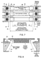
- FIGS. 7 and 8 illustrate an alternative embodiment of the invention formed by steps virtually identical to the steps shown in FIGS. 4-6G except that the ink feed hole etch of the thin film layers extends across the center portion of the printhead, and the orifice layer 85 is used to define ink hole boundaries.
- the ink feed hole mask 86 extends between two opposing ink ejection chambers 30, and the frontside protection mask 88 is slightly larger. Narrow thin film walls separate the etched areas in the central portion of the printhead.
- FIGS. 9 and 10 illustrate a variation of the structures of FIGS. 7 and 8, where an ink feed hole mask 92, followed by an etch, is used to form a large central rectangular opening 98 in the thin film layers 22.
- a frontside protection mask 94 is used to form the protection layer 96 (FIG. 10).
- the orifice layer 85 forms part of the boundary of the ink feed holes.
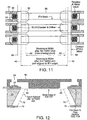
- FIGS. 11 and 12 illustrate a variation of the processes described above, where no separate protection layer is formed.
- the FOX layer 46 (also shown in FIG. 6A) acts as the protection layer in the ink feed hole areas.
- the thin film layers are etched only down to the FOX layer 46, using conventional techniques. After the first trench etch, the trench walls 78 are only roughly aligned with the ink feed holes.
- the exposed FOX layer 46 is then removed using a BOE or other suitable etch (the removed FOX layer is shown in ghost outline in FIG. 12).
- a second trench etch is performed, as before, resulting in the trench walls being aligned with the thin film openings.
- the ink feed hole mask 86 is shown to be similar to that of FIG. 7, the ink feed hole masks of FIGS. 3 and 9 may also be used.
- the process of FIGS. 11 and 12 saves considerable expense in processing wafers by deleting the formation of a separate protection layer.
- a short membrane shelf hanging over the trench walls is shown in the various figures to illustrate that the second etch time is not critical. After the trench walls have been etched past the thin film openings, the etch of the substrate slows considerably.
- FIG. 13 illustrates one embodiment of an inkjet printer 130 that can incorporate the invention. Numerous other designs of inkjet printers may also be used along with this invention. More detail of an inkjet printer is found in U.S. Patent No. 5,852,459, to Norman Pawlowski et al., incorporated herein by reference.
- Inkjet printer 130 includes an input tray 132 containing sheets of paper 134 which are forwarded through a print zone 135, using rollers 137, for being printed upon. The paper 134 is then forwarded to an output tray 136.
- a moveable carriage 138 holds print cartridges 140-143, which respectively print cyan (C), black (K), magenta (M), and yellow (Y) ink.
- inks in replaceable ink cartridges 146 are supplied to their associated print cartridges via flexible ink tubes 148.
- the print cartridges may also be the type that hold a substantial supply of fluid and may be refillable or non-refillable.
- the ink supplies are separate from the printhead portions and are removeably mounted on the printheads in the carriage 138.
- the carriage 138 is moved along a scan axis by a conventional belt and pulley system and slides along a slide rod 150.
- the carriage is stationery, and an array of stationary print cartridges print on a moving sheet of paper.
- Printing signals from a conventional external computer are processed by printer 130 to generate a bitmap of the dots to be printed.
- the bitmap is then converted into firing signals for the printheads.
- the position of the carriage 138 as it traverses back and forth along the scan axis while printing is determined from an optical encoder strip 152, detected by a photoelectric element on carriage 138, to cause the various ink ejection elements on each print cartridge to be selectively fired at the appropriate time during a carriage scan.
- the printhead may use resistive, piezoelectric, or other types of ink ejection elements.
- the print cartridges in carriage 138 scan across a sheet of paper, the swaths printed by the print cartridges overlap. After one or more scans, the sheet of paper 134 is shifted in a direction towards the output tray 136, and the carriage 138 resumes scanning.
- the present invention is equally applicable to alternative printing systems (not shown) that utilize alternative media and/or printhead moving mechanisms, such as those incorporating grit wheel, roll feed, or drum or vacuum belt technology to support and move the print media relative to the printhead assemblies.
- a grit wheel design a grit wheel and pinch roller move the media back and forth along one axis while a carriage carrying one or more printhead assemblies scans past the media along an orthogonal axis.
- a drum printer design the media is mounted to a rotating drum that is rotated along one axis while a carriage carrying one or more printhead assemblies scans past the media along an orthogonal axis. In either the drum or grit wheel designs, the scanning is typically not done in a back and forth manner as is the case for the system depicted in FIG. 13.
- printheads may be formed on a single substrate. Further, an array of printheads may extend across the entire width of a page so that no scanning of the printheads is needed; only the paper is shifted perpendicular to the array.
- Additional print cartridges in the carriage may include other colors or fixers.
Description
- This invention relates to inkjet printers and, more particularly, to a monolithic printhead for an inkjet printer.
- Inkjet printers typically have a printhead mounted on a carriage that scans back and forth across the width of a sheet of paper feeding through the printer. Ink from an ink reservoir, either on-board the carriage or external to the carriage, is fed to ink ejection chambers on the printhead. Each ink ejection chamber contains an ink ejection element, such as a heater resistor or a piezoelectric element, which is independently addressable. Energizing an ink ejection element causes a droplet of ink to be ejected through a nozzle for creating a small dot on the medium. The pattern of dots created forms an image or text.
- A conventional method of etching a through-hole in a printhead substrate is known from US-A- 4 789 425.
- As the resolutions and printing speeds of printheads increase to meet the demanding needs of the consumer market, new printhead manufacturing techniques and structures are required.
- Described herein is a monolithic printhead formed using integrated circuit techniques. Thin film layers, including a resistive layer, are formed on a top surface of a silicon substrate. The various layers are etched to provide conductive leads to the heater resistor elements. Piezoelectric elements may be used instead of the resistive elements.
- At least one ink feed hole is formed through the thin film layers for each ink ejection chamber. In one embodiment, a protective layer is deposited over the ink feed hole area.
- An orifice layer is formed on the top surface of the thin film layers to define the nozzles and ink ejection chambers. In one embodiment, a photo-definable material is used to form the orifice layer.
- A trench mask is formed on the bottom surface of the substrate. A trench is etched (using, for example, TMAH) through the exposed bottom surface of the substrate. The trench completely etches away portions of the substrate beneath the ink feed holes. The protective layer prevents the TMAH from etching the substrate from the front side through the ink feed hole.
- The protective layer is then removed, and a second trench etch is performed. The TMAH solution etches away the substrate portion exposed through the ink feed holes. The second trench etch inherently aligns the edge of the trench with the ink feed holes. This two-step trench etch eases the tolerances for the trench mask and results in a precisely positioned trench, since the trench side walls are ultimately aligned to the thin film openings.
- In another embodiment, a separate protection layer is not deposited. Instead, a field oxide (FOX) layer, formed over the substrate as one of the thin film layers, is used for protection. The ink feed holes are etched through the thin film layers down to the FOX layer. A first trench etch is conducted as in the previous embodiment.
The portions of the FOX layer in the ink feed hole areas are removed with a buffered oxide etch. A second trench etch is then performed that self-aligns the trench sidewalls to the thin film openings. This process is more economical than the previous embodiment using a separate protection layer. - The resulting fully integrated thermal inkjet printhead can be manufactured to a very precise tolerance since the entire structure is monolithic, meeting the needs for the next generation of printheads.
- The process may be used to form openings in devices other than printheads.
-
- FIG. 1 is a perspective view of one embodiment of a print cartridge that may incorporate any one of the printheads described herein.
- FIG. 2 is a perspective cutaway view of a portion of one embodiment of a printhead in accordance with the present invention.
- FIG. 3 is a top down partially transparent view of the printhead shown in FIG. 2, showing additional portions of the printhead.
- FIG. 4 is a cross-sectional view along line 4-4 in FIG. 2 showing additional portions of the printhead.
- FIG. 5 is a cross-sectional view of the printhead portion of FIG. 2 along line 4-4 showing additional detail of the thin film layers.
- FIGS. 6A-6G are cross-sectional views of a portion of the printhead of FIG. 4 along line 4-4 during various stages of the manufacturing process.
- FIG. 7 is a top down partially transparent view of a second embodiment of a printhead.
- FIG. 8 is a cross-sectional view of the second embodiment printhead.
- FIGS. 9 and 10 illustrate a variation of the structures of FIGS. 7 and 8, where a central rectangular ink feed area is formed through the thin film layers.
- FIGS. 11 and 12 illustrate a further variation of the structures of FIGS. 7 and 8, where, instead of a separate protection layer being formed, the FOX layer is used as the protection layer.
- FIG. 13 is a perspective view of a conventional inkjet printer into which the printheads of the present invention may be installed for printing on a medium.
-
- FIG. 1 is a perspective view of one type of
inkjet print cartridge 10 which may incorporate the printhead structures of the present invention. Theprint cartridge 10 of FIG. 1 is the type that contains a substantial quantity of ink within itsbody 12, but another suitable print cartridge may be the type that receives ink from an external ink supply either mounted on the printhead or connected to the printhead via a tube. - The ink is supplied to a
printhead 14.Printhead 14, to be described in detail later, channels the ink into ink ejection chambers, each chamber containing an ink ejection element. Electrical signals are provided tocontacts 16 to individually energize the ink ejection elements to eject a droplet of ink through an associatednozzle 18. The structure and operation of conventional print cartridges are very well known. - FIG. 2 is a cross-sectional view of a portion of the printhead of FIG. 1 taken along line 2-2 in FIG. 1. Although a printhead may have 300 or more nozzles and associated ink ejection chambers, detail of only a single ink ejection chamber need be described in order to understand the invention. It should also be understood by those skilled in the art that many printheads are formed on a single silicon wafer and then separated from one another using conventional techniques.
- In FIG. 2, a
silicon substrate 20 has formed on it variousthin film layers 22, to be described in detail later. Thethin film layers 22 include a resistive layer for formingresistors 24. Other thin film layers perform various functions, such as providing electrical insulation from thesubstrate 20, providing a thermally conductive path from the heater resistor elements to thesubstrate 20, and providing electrical conductors to the resistor elements. Oneelectrical conductor 25 is shown leading to one end of aresistor 24. A similar conductor leads to the other end of theresistor 24. In an actual embodiment, the resistors and conductors in a chamber would be obscured by overlying layers. - Ink feed holes 26 are formed completely through the thin film layers 22. There may be multiple holes per chamber. Alternately, a manifold may be formed in the
orifice layer 28 for providing a common ink channel for a row ofink ejection chambers 30 - An
orifice layer 28 is deposited over the surface of the thin film layers 22 and etched to formink ejection chambers 30, one chamber perresistor 24.Nozzles 34 may be formed using conventional photolithographic techniques. - The
silicon substrate 20 is etched to form atrench 36 extending along the length of the row of ink feed holes 26 so thatink 38 from an ink reservoir may enter the ink feed holes 26 for supplying ink to theink ejection chambers 30. A two-step etch process, described below, is used to precisely align the edges of thetrench 36 with the ink feed holes 26. - In one embodiment, each printhead is approximately one-half inch long and contains two offset rows of nozzles, each row containing 150 nozzles for a total of 300 nozzles per printhead. The printhead can thus print at a single pass resolution of 600 dots per inch (dpi) along the direction of the nozzle rows or print at a greater resolution in multiple passes. Greater resolutions may also be printed along the scan direction of the printhead. Resolutions of 1200 or greater dpi may be obtained using the present invention.
- In operation, an electrical signal is provided to
heater resistor 24, which vaporizes a portion of the ink to form a bubble within theink ejection chamber 30. The bubble propels an ink droplet through an associatednozzle 34 onto a medium. The ink ejection chamber is then refilled by capillary action. - FIG. 3 is a top down view of the printhead of FIG. 2 showing two parallel arrays of ink ejection chambers formed in the printhead. The
ink ejection chambers 30 in the two rows may be offset. Elements in the various figures designated with the same numerals may be similar or identical. - The thin film layer shelf above the trench is referred to as a membrane. The width of this membrane is shown in FIG. 3 by the dashed lines 40. The particular method for forming the printhead of FIG. 2 uses a two-step trench etch process. The first trench etch results in a membrane width, shown by
dash lines 42, that is narrower than thefinal membrane width 40. As will described below, this allows the mask for the first trench etch to have a very relaxed tolerance. The trench sidewalls after the second trench etch are self-aligned to the ink feed holes 26 defined by the thin film layers. - FIG. 4 is a cross-sectional view along line 4-4 in FIG. 2, showing the additional portion of the printhead containing the second row of ink ejection chambers. The thin film layers 22, including the
resistors 24, are shown simplified. Additional detail of FIG. 4 will be discussed with respect to FIGS. 5 and 6A-6G. - FIG. 5 is a cross-sectional view along line 4-4 of FIG. 2 showing a single ink ejection chamber and the associated structure of the printhead. FIG. 5 shows one embodiment of the individual thin film layers, and FIGs. 6A-6G show various steps used to fabricate the printhead of FIGS. 2-5. Conventional deposition, masking, and etching steps are used unless otherwise noted.
- In FIG. 6A, a
silicon substrate 20 with a crystalline orientation of <100> is placed in a vacuum chamber. The bulk silicon is about 675 microns thick. - A
field oxide layer 46, having a thickness of 1.2 microns, is formed over thesilicon substrate 20 using conventional techniques. A phosphosilicate glass (PSG)layer 48, having a thickness of 0.5 microns, is then deposited over thefield oxide layer 46 using conventional techniques. - A
mask 49 is formed over thePSG layer 48 using conventional photolithographic techniques. Themask 49 is also shown in FIGS. 3 and 7. ThePSG layer 48 is then etched using conventional reactive ion etching (RIE) to pull back thePSG layer 48 from the subsequently formed ink feed hole. This will protect thePSG layer 48 from ink. - A boron PSG or boron TEOS (BTEOS) layer may be used instead of
PSG layer 48 and etched in a manner similar to the etching oflayer 48. - In FIG. 6B,
mask 49 is removed and aresistive layer 50 of, for example, tantalum aluminum (TaAl), having a thickness of 0.1 microns, is then the deposited over thePSG layer 48. Other known resistive layers can also be used. Aconductive layer 25 of AlCu is then deposited over the TaAl. Amask 54 is deposited and patterned using conventional photolithographic techniques, and theconductive layer 25 and theresistive layer 50 are etched using conventional IC fabrication techniques. Another masking and etching step (not shown) is used to remove the portions of the AlCu over theheater resistors 24, as shown in FIG. 2. The resulting AlCu conductors are outside the field of view of FIGS. 6A-6G. - The etching of the
conductive layer 25 andresistive layer 50 define a first resistor dimension (e.g., a width). A second resistor dimension (e.g., a length) is defined by etching theconductive layer 25 to cause the resistive portion to be contacted by the conductive traces at two ends. This technique of forming resistors and electrical conductors is well known in the art. The conductive traces are formed so as to not extend across the middle of the printhead, but run along the edges. Appropriate addressing circuitry and pads are provided on thesubstrate 20 for providing energizing signals to theresistors 24. - In FIG. 6C, over the
resistors 24 andconductive layer 25 is formed asilicon nitride layer 56, having a thickness of 0.5 microns. This layer provides insulation and passivation. - Over the
nitride layer 56 is formed asilicon carbide layer 58, having a thickness of 0.25 microns, to provide additional insulation and passivation. Thenitride layer 56 andcarbide layer 58 now protect thePSG layer 48 from the ink and etchant. Other dielectric layers may be used instead of nitride and carbide. - The passivation layers are then masked (outside the field of view) and etched using conventional techniques to expose portions of the
conductive layer 25 for electrical contact to a subsequent gold conductive layer to provide ground lines. - A
bubble cavitation layer 60 of tantalum (Ta) is then formed over thecarbide layer 58. Gold (Au) 62 is deposited over thetantalum layer 60 and etched to form the ground lines electrically connected to certain ones of theconductive layer 25 traces. The ground lines terminate in bond pads along edges of thesubstrate 20. - The AlCu and gold conductors may be coupled to transistors formed on the substrate surface. Such transistors are described in U.S. Patent No. 5,648,806, previously mentioned.
- In FIG. 6D, a
mask 66 is patterned to expose a portion of the thin film layers to be etched to form the ink feed holes 26 (FIG. 2). Alternately, multiple masking and etching steps may be used as the various thin film layers are formed to etch the ink feed holes. - The thin film layers are then etched using an anisotropic etch. This ink feed hole etch process can be a combination of several types of etches (RIE or wet). The etch through the thin film layers may use conventional IC fabrication techniques. The resulting wafer after the etch is shown in FIG. 6E.
- When forming the
trench 36 of FIG. 2, it is difficult to perfectly align the backside trench mask with the ink feed holes 26. The manufacturing process described below includes a technique to align thetrench 36 with the ink feed holes 26. - In FIG. 6F, a
frontside protection layer 70 is deposited and formed using conventional photolithographic techniques. In one embodiment, theprotection layer 70 is a plasma TEOS having a thickness (e.g., 1000 angstroms) that is thin enough so that it can be quickly and easily removed by a buffered oxide etch (BOE) but thick enough that it can withstand exposure to the TMAH (tetramethyl ammonium hydroxide) etchant throughout the approximately fifteen hour trench etch. Theprotection layer 70 may be any suitable material, including oxides, nitrides, and oxinitrides. A mask for this operation would be the inverse of the ink feed hole mask and biased slightly larger to ensure that the entire ink feed hole opening remains covered with aprotection layer 70. FIG. 3 shows theprotection layer 70 mask boundary. - Referring to FIG. 6G, an
orifice layer 28 is then deposited and formed. Theorifice layer 28 may be formed of a spun-on epoxy called SU8.Orifice layer 28 may alternatively be laminated or screened on. The orifice layer in one embodiment is about 20 microns. The ink chambers 30 (FIG. 2) andnozzles 34 are formed through photolithography. In one technique, a first mask using a half dosage of UV radiation "hardens" the upper surface of the SU8 except in locations where thenozzles 34 are to be formed. A second mask using a full UV dosage then exposes the SU8 in those areas where neithernozzles 34 norink ejection chambers 30 are to be formed. After these two exposures, the SU8 is developed, and the hardened portions remain but the nozzle portions and the ink ejection chamber portions of the SU8 are removed. - The thin film layers and formed
orifice layer 28 are shown in FIG. 4. - The backside of the wafer is then masked (by mask 76) using conventional techniques to expose the portion of the backside of the wafer to be subjected to the TMAH trench etch. The
backside mask 76 may be a FOX hardmask formed using conventional photolithographic techniques. The wafer is dipped into the wet TMAH etch, which forms the angled profile (also defined by the dashed lines 78) shown in FIG. 4. This first etch is conducted for a time sufficient to etch through to theFOX layer 46 and theprotection layer 70. The dashedline 78 portion of the trench walls after the first etch extends up to within the ink feed hole area. The resulting membrane width between the trench walls is shown in FIG. 3 by the dashed lines 42. The trench width will typically be less than 200 microns, and, in one embodiment, is between 20-60 microns. The backside masking may be misaligned by a large margin. Such misalignment would normally restrict the area of the ink feed hole and have an adverse effect on the fluid properties of the printhead. However, the process described below avoids any adverse effects of such misalignment. - The wafer is then placed in a BOE solution that removes the
protection layer 70. A "ghost" image of theprotection layer 70 is shown in FIG. 4. - The wafer is again subjected to a TMAH wet etch, where the etchant now contacts the portion of the silicon revealed through the ink feed holes 26. This inherently produces the angled etch self-aligned with the edge of the
ink feed hole 26, shown in FIG. 4. During this second trench etch, the trench widens at a rapid rate until it reaches the edge of the ink feed holes. FIGs. 3 and 4 intentionally show the first trench etch being misaligned (seelines 42 in FIG. 3) with respect to the ink feed holes 26 to show that the resulting trench, after the second etch, has trench edges aligned with the ink feed holes (seelines 40 in FIG. 3). - The
trench 36, in one embodiment, extends the length of a row of ink ejection chambers. Any one of several etch techniques could be used, wet or dry. Examples of dry etches include XeF2 and SiF6. Examples of appropriate wet etches include ethylene diamine pyrocatecol (EDP), potassium hydroxide (KOH), and TMAH. Other etches may also be used. Any one of these or a combination thereof could be used for this application. - The resulting wafer is then sawed to form the individual printheads. A flexible circuit is used to provide electrical access to the conductors on the printhead. The resulting assembly is then affixed to a plastic print cartridge, such as that shown in FIG. 1, and the printhead is sealed with respect to the print cartridge body to prevent ink seepage.
- In one embodiment, the
orifice layer 28 is formed to also provideposts 80, 82 (FIG. 4) for blocking relatively large ink particles from entering into thechamber 30. FIG. 3 illustrates four such posts in dashed outline for each chamber. Theposts chambers 30. - The
trench 36 may extend the length of the printhead or, to improve the mechanical strength of the printhead, only extend a portion of the length of the printhead beneath the ink ejection chambers. A passivation layer may be deposited on thesubstrate 20 if reaction of the substrate with the ink is a concern. - FIGS. 7 and 8 illustrate an alternative embodiment of the invention formed by steps virtually identical to the steps shown in FIGS. 4-6G except that the ink feed hole etch of the thin film layers extends across the center portion of the printhead, and the
orifice layer 85 is used to define ink hole boundaries. - As seen in FIG. 7, the ink
feed hole mask 86 extends between two opposingink ejection chambers 30, and thefrontside protection mask 88 is slightly larger. Narrow thin film walls separate the etched areas in the central portion of the printhead. - FIGS. 9 and 10 illustrate a variation of the structures of FIGS. 7 and 8, where an ink
feed hole mask 92, followed by an etch, is used to form a large centralrectangular opening 98 in the thin film layers 22. Afrontside protection mask 94 is used to form the protection layer 96 (FIG. 10). Theorifice layer 85 forms part of the boundary of the ink feed holes. - FIGS. 11 and 12 illustrate a variation of the processes described above, where no separate protection layer is formed. In this process, the FOX layer 46 (also shown in FIG. 6A) acts as the protection layer in the ink feed hole areas. In contrast to FIGS. 7 and 8, the thin film layers are etched only down to the
FOX layer 46, using conventional techniques. After the first trench etch, thetrench walls 78 are only roughly aligned with the ink feed holes. The exposedFOX layer 46 is then removed using a BOE or other suitable etch (the removed FOX layer is shown in ghost outline in FIG. 12). A second trench etch is performed, as before, resulting in the trench walls being aligned with the thin film openings. Although the inkfeed hole mask 86 is shown to be similar to that of FIG. 7, the ink feed hole masks of FIGS. 3 and 9 may also be used. The process of FIGS. 11 and 12 saves considerable expense in processing wafers by deleting the formation of a separate protection layer. - A short membrane shelf hanging over the trench walls is shown in the various figures to illustrate that the second etch time is not critical. After the trench walls have been etched past the thin film openings, the etch of the substrate slows considerably.
- One skilled in the art of integrated circuit manufacturing would understand the various techniques used to form the printhead structures described herein. The thin film layers and their thicknesses may be varied, and some layers deleted, while still obtaining the benefits of the present invention. Additional ink feed hole patterns are also envisioned.
- FIG. 13 illustrates one embodiment of an
inkjet printer 130 that can incorporate the invention. Numerous other designs of inkjet printers may also be used along with this invention. More detail of an inkjet printer is found in U.S. Patent No. 5,852,459, to Norman Pawlowski et al., incorporated herein by reference. -
Inkjet printer 130 includes aninput tray 132 containing sheets ofpaper 134 which are forwarded through aprint zone 135, usingrollers 137, for being printed upon. Thepaper 134 is then forwarded to anoutput tray 136. Amoveable carriage 138 holds print cartridges 140-143, which respectively print cyan (C), black (K), magenta (M), and yellow (Y) ink. - In one embodiment, inks in
replaceable ink cartridges 146 are supplied to their associated print cartridges viaflexible ink tubes 148. The print cartridges may also be the type that hold a substantial supply of fluid and may be refillable or non-refillable. In another embodiment, the ink supplies are separate from the printhead portions and are removeably mounted on the printheads in thecarriage 138. - The
carriage 138 is moved along a scan axis by a conventional belt and pulley system and slides along aslide rod 150. In another embodiment, the carriage is stationery, and an array of stationary print cartridges print on a moving sheet of paper. - Printing signals from a conventional external computer (e.g., a PC) are processed by
printer 130 to generate a bitmap of the dots to be printed. The bitmap is then converted into firing signals for the printheads. The position of thecarriage 138 as it traverses back and forth along the scan axis while printing is determined from anoptical encoder strip 152, detected by a photoelectric element oncarriage 138, to cause the various ink ejection elements on each print cartridge to be selectively fired at the appropriate time during a carriage scan. - The printhead may use resistive, piezoelectric, or other types of ink ejection elements.
- As the print cartridges in
carriage 138 scan across a sheet of paper, the swaths printed by the print cartridges overlap. After one or more scans, the sheet ofpaper 134 is shifted in a direction towards theoutput tray 136, and thecarriage 138 resumes scanning. - The present invention is equally applicable to alternative printing systems (not shown) that utilize alternative media and/or printhead moving mechanisms, such as those incorporating grit wheel, roll feed, or drum or vacuum belt technology to support and move the print media relative to the printhead assemblies. With a grit wheel design, a grit wheel and pinch roller move the media back and forth along one axis while a carriage carrying one or more printhead assemblies scans past the media along an orthogonal axis. With a drum printer design, the media is mounted to a rotating drum that is rotated along one axis while a carriage carrying one or more printhead assemblies scans past the media along an orthogonal axis. In either the drum or grit wheel designs, the scanning is typically not done in a back and forth manner as is the case for the system depicted in FIG. 13.
- Multiple printheads may be formed on a single substrate. Further, an array of printheads may extend across the entire width of a page so that no scanning of the printheads is needed; only the paper is shifted perpendicular to the array.
- Additional print cartridges in the carriage may include other colors or fixers.
Claims (29)
- A method for forming a printing device comprising:providing a printhead substrate (20);forming a plurality of thin film layers (22) on a first surface of said substrate, at least one of said layers forming a plurality of ink ejection elements (24);forming ink feed openings (26) through at least some of said thin film layers;providing a protection layer (46, 70, 96) between said ink feed openings and said substrate;masking (76) a second surface of said substrate to perform a trench etch;etching said second surface of said substrate to form a first trench portion (78);removing said protection layer at least between said ink feed openings and said substrate; andfurther etching said portions of said substrate exposed through said ink feed openings to self-align edges of said trench (36) substantially to said ink feed openings.
- The method of Claim 1 wherein said thin film layers (22) include a field oxide layer (46), said protection layer being a portion of said field oxide layer remaining after said thin film layers are etched to form said ink feed openings (26).
- The method of Claim 1 wherein said providing a protection layer comprises forming a protection layer (70, 96) within said ink feed openings (26) after said ink feed openings are formed.
- The method of Claim 1 wherein said forming ink feed openings (26) comprises forming openings completely through said thin film layers (22).
- The method of Claim 1 further comprising forming an orifice layer (28, 85) over said thin film layers (22), said orifice layer defining a plurality of ink ejection chambers (30), each chamber having within it an ink ejection element (24), said orifice layer further defining a nozzle (34) for each ink ejection chamber.
- The method of Claim 5 wherein said removing said protection layer (46, 70, 96) comprises performing a wet etch such that a wet etchant enters said chambers (30) and etches said protection layer.
- The method of Claim 5 wherein a central portion of said orifice layer (28) overlies a thin film membrane.
- The method of Claim 5 wherein said orifice layer (85) defines boundaries of ink feed holes (26) formed in part by said ink feed openings.
- The method of Claim 1 wherein said providing a protection layer (70) comprises depositing TEOS.
- The method of Claim 1 wherein said providing a protection layer (46, 70, 96) comprises depositing material selected from the group consisting of oxides, nitrides, and oxinitrides.
- The method of Claim 1 wherein said providing a protection layer comprises forming a protection layer (46, 70, 96) over an area greater than an ink feed opening area.
- The method of Claim 1 wherein said forming ink feed openings (26) comprises forming ink feed openings only in the vicinity of each ink ejection element (24).
- The method of Claim 1 wherein forming ink feed openings (26) comprises forming elongated ink feed openings (86) extending across a central portion of said substrate (20).
- The method of Claim 1 wherein forming ink feed openings (26) comprising forming a rectangular ink feed opening (92) in a central portion of said substrate (20).
- The method of Claim 1 wherein a bottom layer (46) of thin film layers, directly adjacent said substrate, and said protection layer (46, 70, 96) act as an etch stop for said etching said second surface of said substrate to form said first trench portion (78).
- The method of Claim 1 wherein said etching said second surface of said substrate (20) to form a first trench portion (78) comprises etching said substrate with a TMAH solution to form an angled trench edge with respect to said second surface.
- A printhead during fabrication comprising:a printhead substrate (20);a plurality of thin film layers (22) formed on a first surface of said substrate, at least one of said layers forming a plurality of ink ejection elements (24);ink feed openings (26) formed through at least some of said thin film layers;a protection layer (46, 70, 96) between said ink feed openings and said substrate;a trench (78) etched through said substrate to said protection layer between said ink feed openings and said substrate, said protection layer between said ink feed openings and said substrate for being removed followed by a second trench etch to form a trench having walls substantially aligned with said ink feed openings.
- The device of Claim 17 wherein said thin film layers include a field oxide layer (46), said protection layer being a portion of said field oxide layer remaining after said thin film layers (22) are etched.
- The device of Claim 17 wherein said protection layer (70, 96) is formed within said ink feed openings after said ink feed openings (26) are formed.
- The device of Claim 17 wherein said ink feed openings (26) are formed completely through said thin film layers (22).
- The device of Claim 17 further comprising an orifice layer (28, 85) formed over said thin film layers, said orifice layer defining a plurality of ink ejection chambers, each chamber having within it an ink ejection element, said orifice layer further defining a nozzle for each ink ejection chamber.
- A method for forming a through hole comprising:providing a substrate (20);forming a plurality of thin film layers (22) on a first surface of said substrate;forming openings (26) through at least some of said thin film layers;providing a protection layer (46, 70, 96) between said openings and said substrate;masking (76) a second surface of said substrate to perform a trench etch;etching said second surface of said substrate to form a first trench portion (78);removing said protection layer between said openings and said substrate; andfurther etching said portions of said substrate exposed through said openings to self-align edges of said trench (36) substantially to said openings.
- The method of Claim 22 wherein said thin film layers (22) include a field oxide layer (46), said protection layer being a portion of said field oxide layer remaining after said thin film layers are etched to form said openings (26).
- The method of Claim 22 wherein said providing a protection layer comprises forming a protection layer (70, 96) within said openings after said openings are formed.
- The method of Claim 22 wherein said forming openings (26) comprises forming openings completely through said thin film layers (22).
- The method of Claim 22 wherein said providing a protection layer (70, 96) comprises depositing TEOS.
- The method of Claim 22 wherein said providing a protection layer (46, 70, 96) comprises depositing material selected from the group consisting of oxides, nitrides, and oxinitrides.
- The method of Claim 22 wherein said providing a protection layer comprises forming a protection layer (46, 70, 96) over an area greater than an opening area.
- The method of Claim 22 wherein said etching said second surface of said substrate (20) to form a first trench portion (78) comprises etching said substrate with a TMAH solution to form an angled trench edge with respect to said second surface.
Applications Claiming Priority (2)
| Application Number | Priority Date | Filing Date | Title |
|---|---|---|---|
| US770723 | 2001-01-25 | ||
| US09/770,723 US6419346B1 (en) | 2001-01-25 | 2001-01-25 | Two-step trench etch for a fully integrated thermal inkjet printhead |
Publications (3)
| Publication Number | Publication Date |
|---|---|
| EP1226946A2 EP1226946A2 (en) | 2002-07-31 |
| EP1226946A3 EP1226946A3 (en) | 2003-07-23 |
| EP1226946B1 true EP1226946B1 (en) | 2005-12-21 |
Family
ID=25089474
Family Applications (1)
| Application Number | Title | Priority Date | Filing Date |
|---|---|---|---|
| EP02250340A Expired - Lifetime EP1226946B1 (en) | 2001-01-25 | 2002-01-18 | Two-step trench etch for a fully integrated thermal inkjet printhead |
Country Status (4)
| Country | Link |
|---|---|
| US (2) | US6419346B1 (en) |
| EP (1) | EP1226946B1 (en) |
| JP (1) | JP3980361B2 (en) |
| DE (1) | DE60208088T2 (en) |
Families Citing this family (27)
| Publication number | Priority date | Publication date | Assignee | Title |
|---|---|---|---|---|
| US6481832B2 (en) | 2001-01-29 | 2002-11-19 | Hewlett-Packard Company | Fluid-jet ejection device |
| US6626523B2 (en) * | 2001-10-31 | 2003-09-30 | Hewlett-Packard Development Company, Lp. | Printhead having a thin film membrane with a floating section |
| US6908784B1 (en) * | 2002-03-06 | 2005-06-21 | Micron Technology, Inc. | Method for fabricating encapsulated semiconductor components |
| KR100484168B1 (en) | 2002-10-11 | 2005-04-19 | 삼성전자주식회사 | Ink jet printhead and manufacturing method thereof |
| KR100499132B1 (en) | 2002-10-24 | 2005-07-04 | 삼성전자주식회사 | Inkjet printhead and manufacturing method thereof |
| US6648454B1 (en) * | 2002-10-30 | 2003-11-18 | Hewlett-Packard Development Company, L.P. | Slotted substrate and method of making |
| KR100459905B1 (en) * | 2002-11-21 | 2004-12-03 | 삼성전자주식회사 | Monolithic inkjet printhead having heater disposed between dual ink chamber and method of manufacturing thereof |
| KR100468160B1 (en) * | 2002-12-02 | 2005-01-26 | 삼성전자주식회사 | monolithic bubble-ink jet print head and fabrication method therefor |
| KR100477707B1 (en) * | 2003-05-13 | 2005-03-18 | 삼성전자주식회사 | Method of manufacturing Monolithic inkjet printhead |
| US7036913B2 (en) | 2003-05-27 | 2006-05-02 | Samsung Electronics Co., Ltd. | Ink-jet printhead |
| KR100517515B1 (en) | 2004-01-20 | 2005-09-28 | 삼성전자주식회사 | Method for manufacturing monolithic inkjet printhead |
| GB2410464A (en) * | 2004-01-29 | 2005-08-03 | Hewlett Packard Development Co | A method of making an inkjet printhead |
| US20050260522A1 (en) * | 2004-02-13 | 2005-11-24 | William Weber | Permanent resist composition, cured product thereof, and use thereof |
| US7449280B2 (en) * | 2004-05-26 | 2008-11-11 | Microchem Corp. | Photoimageable coating composition and composite article thereof |
| KR100765315B1 (en) | 2004-07-23 | 2007-10-09 | 삼성전자주식회사 | ink jet head including filtering element formed in a single body with substrate and method of fabricating the same |
| US8043517B2 (en) * | 2005-09-19 | 2011-10-25 | Hewlett-Packard Development Company, L.P. | Method of forming openings in substrates and inkjet printheads fabricated thereby |
| KR20080046865A (en) * | 2006-11-23 | 2008-05-28 | 삼성전자주식회사 | Head chip and ink cartridge for image forimg apparatus having the same |
| EP2091741B1 (en) | 2006-12-07 | 2011-08-24 | Hewlett-Packard Development Company, L.P. | Method of forming openings in substrates |
| US8241510B2 (en) * | 2007-01-22 | 2012-08-14 | Canon Kabushiki Kaisha | Inkjet recording head, method for producing same, and semiconductor device |
| KR20090024381A (en) * | 2007-09-04 | 2009-03-09 | 삼성전자주식회사 | Inkjet print head |
| JP5854693B2 (en) * | 2010-09-01 | 2016-02-09 | キヤノン株式会社 | Method for manufacturing liquid discharge head |
| WO2014018008A1 (en) * | 2012-07-24 | 2014-01-30 | Hewlett-Packard Company, L.P. | Fluid ejection device with particle tolerant thin-film extension |
| JP6103879B2 (en) * | 2012-10-24 | 2017-03-29 | キヤノン株式会社 | Method for manufacturing liquid discharge head |
| US9707754B2 (en) | 2012-12-20 | 2017-07-18 | Hewlett-Packard Development Company, L.P. | Fluid ejection device with particle tolerant layer extension |
| US9776409B2 (en) | 2014-04-24 | 2017-10-03 | Hewlett-Packard Development Company, L.P. | Fluidic ejection device with layers having different light sensitivities |
| EP3429856B1 (en) * | 2016-07-26 | 2022-01-12 | Hewlett-Packard Development Company, L.P. | Fluid ejection device with a portioning wall |
| JP7066418B2 (en) * | 2018-01-17 | 2022-05-13 | キヤノン株式会社 | Liquid discharge head and its manufacturing method |
Family Cites Families (6)
| Publication number | Priority date | Publication date | Assignee | Title |
|---|---|---|---|---|
| EP0244214B1 (en) | 1986-04-28 | 1991-07-10 | Hewlett-Packard Company | Thermal ink jet printhead |
| US4789425A (en) * | 1987-08-06 | 1988-12-06 | Xerox Corporation | Thermal ink jet printhead fabricating process |
| US5648806A (en) | 1992-04-02 | 1997-07-15 | Hewlett-Packard Company | Stable substrate structure for a wide swath nozzle array in a high resolution inkjet printer |
| DE69730667T2 (en) | 1996-11-11 | 2005-09-22 | Canon K.K. | A method of making a via, use of this method of making a silicon substrate having such a via, or apparatus with that substrate, methods of making an inkjet printhead, and use of this method of making an inkjet printhead |
| US6022482A (en) * | 1997-08-04 | 2000-02-08 | Xerox Corporation | Monolithic ink jet printhead |
| JP3408130B2 (en) * | 1997-12-19 | 2003-05-19 | キヤノン株式会社 | Ink jet recording head and method of manufacturing the same |
-
2001
- 2001-01-25 US US09/770,723 patent/US6419346B1/en not_active Expired - Lifetime
-
2002
- 2002-01-18 DE DE60208088T patent/DE60208088T2/en not_active Expired - Lifetime
- 2002-01-18 EP EP02250340A patent/EP1226946B1/en not_active Expired - Lifetime
- 2002-01-24 JP JP2002016080A patent/JP3980361B2/en not_active Expired - Fee Related
- 2002-06-27 US US10/185,532 patent/US20020167553A1/en not_active Abandoned
Also Published As
| Publication number | Publication date |
|---|---|
| EP1226946A3 (en) | 2003-07-23 |
| JP2002254662A (en) | 2002-09-11 |
| DE60208088T2 (en) | 2006-08-24 |
| JP3980361B2 (en) | 2007-09-26 |
| DE60208088D1 (en) | 2006-01-26 |
| EP1226946A2 (en) | 2002-07-31 |
| US6419346B1 (en) | 2002-07-16 |
| US20020097302A1 (en) | 2002-07-25 |
| US20020167553A1 (en) | 2002-11-14 |
Similar Documents
| Publication | Publication Date | Title |
|---|---|---|
| EP1226946B1 (en) | Two-step trench etch for a fully integrated thermal inkjet printhead | |
| EP1078755B1 (en) | Fully integrated thermal inkjet printhead having multiple ink feed holes per nozzle | |
| US6938340B2 (en) | Method of forming a printhead using a silicon on insulator substrate | |
| US6543884B1 (en) | Fully integrated thermal inkjet printhead having etched back PSG layer | |
| EP1078753B1 (en) | Fully integrated thermal inkjet printhead having thin film layer shelf | |
| EP1211076B1 (en) | Ink-feed channel structure for fully integrated ink-jet printhead | |
| EP1308283B1 (en) | Printhead having a thin film membrane with a floating section | |
| EP1241009B1 (en) | Ink feed trench etch technique for a fully integrated thermal inkjet printhead | |
| US6234623B1 (en) | Integral ink filter for ink jet printhead | |
| US6782621B2 (en) | Method of fabricating a fluid ejector |
Legal Events
| Date | Code | Title | Description |
|---|---|---|---|
| PUAI | Public reference made under article 153(3) epc to a published international application that has entered the european phase |
Free format text: ORIGINAL CODE: 0009012 |
|
| AK | Designated contracting states |
Kind code of ref document: A2 Designated state(s): AT BE CH CY DE DK ES FI FR GB GR IE IT LI LU MC NL PT SE TR |
|
| AX | Request for extension of the european patent |
Free format text: AL;LT;LV;MK;RO;SI |
|
| PUAL | Search report despatched |
Free format text: ORIGINAL CODE: 0009013 |
|
| AK | Designated contracting states |
Designated state(s): AT BE CH CY DE DK ES FI FR GB GR IE IT LI LU MC NL PT SE TR |
|
| AX | Request for extension of the european patent |
Extension state: AL LT LV MK RO SI |
|
| 17P | Request for examination filed |
Effective date: 20030911 |
|
| AKX | Designation fees paid |
Designated state(s): DE FR GB NL |
|
| GRAP | Despatch of communication of intention to grant a patent |
Free format text: ORIGINAL CODE: EPIDOSNIGR1 |
|
| GRAS | Grant fee paid |
Free format text: ORIGINAL CODE: EPIDOSNIGR3 |
|
| GRAA | (expected) grant |
Free format text: ORIGINAL CODE: 0009210 |
|
| AK | Designated contracting states |
Kind code of ref document: B1 Designated state(s): DE FR GB NL |
|
| REG | Reference to a national code |
Ref country code: GB Ref legal event code: FG4D |
|
| REF | Corresponds to: |
Ref document number: 60208088 Country of ref document: DE Date of ref document: 20060126 Kind code of ref document: P |
|
| ET | Fr: translation filed | ||
| PLBE | No opposition filed within time limit |
Free format text: ORIGINAL CODE: 0009261 |
|
| STAA | Information on the status of an ep patent application or granted ep patent |
Free format text: STATUS: NO OPPOSITION FILED WITHIN TIME LIMIT |
|
| 26N | No opposition filed |
Effective date: 20060922 |
|
| REG | Reference to a national code |
Ref country code: GB Ref legal event code: 732E Free format text: REGISTERED BETWEEN 20120329 AND 20120404 |
|
| REG | Reference to a national code |
Ref country code: NL Ref legal event code: SD Effective date: 20120731 |
|
| REG | Reference to a national code |
Ref country code: FR Ref legal event code: PLFP Year of fee payment: 15 |
|
| REG | Reference to a national code |
Ref country code: FR Ref legal event code: PLFP Year of fee payment: 16 |
|
| REG | Reference to a national code |
Ref country code: FR Ref legal event code: PLFP Year of fee payment: 17 |
|
| PGFP | Annual fee paid to national office [announced via postgrant information from national office to epo] |
Ref country code: NL Payment date: 20181221 Year of fee payment: 18 |
|
| PGFP | Annual fee paid to national office [announced via postgrant information from national office to epo] |
Ref country code: GB Payment date: 20181219 Year of fee payment: 18 Ref country code: FR Payment date: 20181220 Year of fee payment: 18 |
|
| PGFP | Annual fee paid to national office [announced via postgrant information from national office to epo] |
Ref country code: DE Payment date: 20181218 Year of fee payment: 18 |
|
| REG | Reference to a national code |
Ref country code: DE Ref legal event code: R119 Ref document number: 60208088 Country of ref document: DE |
|
| REG | Reference to a national code |
Ref country code: NL Ref legal event code: MM Effective date: 20200201 |
|
| GBPC | Gb: european patent ceased through non-payment of renewal fee |
Effective date: 20200118 |
|
| PG25 | Lapsed in a contracting state [announced via postgrant information from national office to epo] |
Ref country code: GB Free format text: LAPSE BECAUSE OF NON-PAYMENT OF DUE FEES Effective date: 20200118 Ref country code: FR Free format text: LAPSE BECAUSE OF NON-PAYMENT OF DUE FEES Effective date: 20200131 Ref country code: DE Free format text: LAPSE BECAUSE OF NON-PAYMENT OF DUE FEES Effective date: 20200801 Ref country code: NL Free format text: LAPSE BECAUSE OF NON-PAYMENT OF DUE FEES Effective date: 20200201 |