EP1225627A2 - Semiconductor integrated circuit device and manufacture method therefor - Google Patents
Semiconductor integrated circuit device and manufacture method therefor Download PDFInfo
- Publication number
- EP1225627A2 EP1225627A2 EP02250303A EP02250303A EP1225627A2 EP 1225627 A2 EP1225627 A2 EP 1225627A2 EP 02250303 A EP02250303 A EP 02250303A EP 02250303 A EP02250303 A EP 02250303A EP 1225627 A2 EP1225627 A2 EP 1225627A2
- Authority
- EP
- European Patent Office
- Prior art keywords
- area
- mos transistor
- conductivity
- type well
- drain
- Prior art date
- Legal status (The legal status is an assumption and is not a legal conclusion. Google has not performed a legal analysis and makes no representation as to the accuracy of the status listed.)
- Granted
Links
Images





Classifications
-
- H—ELECTRICITY
- H10—SEMICONDUCTOR DEVICES; ELECTRIC SOLID-STATE DEVICES NOT OTHERWISE PROVIDED FOR
- H10D—INORGANIC ELECTRIC SEMICONDUCTOR DEVICES
- H10D84/00—Integrated devices formed in or on semiconductor substrates that comprise only semiconducting layers, e.g. on Si wafers or on GaAs-on-Si wafers
- H10D84/80—Integrated devices formed in or on semiconductor substrates that comprise only semiconducting layers, e.g. on Si wafers or on GaAs-on-Si wafers characterised by the integration of at least one component covered by groups H10D12/00 or H10D30/00, e.g. integration of IGFETs
- H10D84/82—Integrated devices formed in or on semiconductor substrates that comprise only semiconducting layers, e.g. on Si wafers or on GaAs-on-Si wafers characterised by the integration of at least one component covered by groups H10D12/00 or H10D30/00, e.g. integration of IGFETs of only field-effect components
- H10D84/83—Integrated devices formed in or on semiconductor substrates that comprise only semiconducting layers, e.g. on Si wafers or on GaAs-on-Si wafers characterised by the integration of at least one component covered by groups H10D12/00 or H10D30/00, e.g. integration of IGFETs of only field-effect components of only insulated-gate FETs [IGFET]
- H10D84/85—Complementary IGFETs, e.g. CMOS
- H10D84/854—Complementary IGFETs, e.g. CMOS comprising arrangements for preventing bipolar actions between the different IGFET regions, e.g. arrangements for latchup prevention
-
- H—ELECTRICITY
- H10—SEMICONDUCTOR DEVICES; ELECTRIC SOLID-STATE DEVICES NOT OTHERWISE PROVIDED FOR
- H10D—INORGANIC ELECTRIC SEMICONDUCTOR DEVICES
- H10D84/00—Integrated devices formed in or on semiconductor substrates that comprise only semiconducting layers, e.g. on Si wafers or on GaAs-on-Si wafers
- H10D84/01—Manufacture or treatment
- H10D84/0123—Integrating together multiple components covered by H10D12/00 or H10D30/00, e.g. integrating multiple IGBTs
- H10D84/0126—Integrating together multiple components covered by H10D12/00 or H10D30/00, e.g. integrating multiple IGBTs the components including insulated gates, e.g. IGFETs
- H10D84/0165—Integrating together multiple components covered by H10D12/00 or H10D30/00, e.g. integrating multiple IGBTs the components including insulated gates, e.g. IGFETs the components including complementary IGFETs, e.g. CMOS devices
- H10D84/017—Manufacturing their source or drain regions, e.g. silicided source or drain regions
-
- H—ELECTRICITY
- H10—SEMICONDUCTOR DEVICES; ELECTRIC SOLID-STATE DEVICES NOT OTHERWISE PROVIDED FOR
- H10D—INORGANIC ELECTRIC SEMICONDUCTOR DEVICES
- H10D84/00—Integrated devices formed in or on semiconductor substrates that comprise only semiconducting layers, e.g. on Si wafers or on GaAs-on-Si wafers
- H10D84/01—Manufacture or treatment
- H10D84/02—Manufacture or treatment characterised by using material-based technologies
- H10D84/03—Manufacture or treatment characterised by using material-based technologies using Group IV technology, e.g. silicon technology or silicon-carbide [SiC] technology
- H10D84/038—Manufacture or treatment characterised by using material-based technologies using Group IV technology, e.g. silicon technology or silicon-carbide [SiC] technology using silicon technology, e.g. SiGe
Definitions
- the present invention relates to a semiconductor integrated circuit device and a manufacture method therefor, and in particular, to a semiconductor integrated circuit device comprising a second-conductivity-type well area on a main surface of a first-conductivity-type semiconductor substrate and a MOSFET formed in a first-conductivity-type well area formed within the second-conductivity-type well area.
- the well-known triple-well NMOS transistor has an N-type well area formed on a main surface of a P-type semiconductor substrate, a P-type well area further formed within the N-type well area, and an NMOSFET formed in the P-type well area (Japanese Patent Application Publication No. 7-78881).
- the triple-well NMOS transistor With the triple-well NMOS transistor, the potentials at a source and a well can be set to be equal, thereby avoiding a back gate bias.
- the NMOS transistor is formed in the P-type well within the N-type well, so that (for example), the N-type well can be set to have the highest potential, while the P-type well can be set to have a lower potential. Consequently, this transistor has the advantage of enabling the use of a negative voltage.
- Japanese Patent Application Publication No. 11-233769 discloses a technique of restraining the occurrence of a punch-through phenomenon in a fine MOSFET by forming an impurity area (punch-through stopper area) deep below a gate electrode, the impurity area having a conductivity type opposite to that of a source and a drain.
- Japanese Patent Application Publication No. 2000-91574 discloses a technique of increasing a drain voltage resistance by forming an offset drain area between a drain area and a channel formed area, the offset drain area having the same conductivity type as the drain area and a lower impurity concentration than the drain area.
- Japanese Patent Application Publication 7-183390 discloses a semiconductor device having a punch-through stopper area and an offset drain area.
- the N-type drain area, the P-type well area, and the N-type well area constitute a parasitic bipolar transistor, so that a parasitic current may flow that corresponds to the amount of injected charge, such as substrate current multiplied by current gain.
- parasitic current may have the adverse effect of increasing current consumption or causing a thermal runaway of the parasitic bipolar transistor, destroying the elements.
- the present invention is provided in view of these problems, and it is an object thereof to provide a semiconductor integrated circuit device comprising a MOS transistor having a triple-well structure, wherein substrate current can be restrained and the current gain of the parasitic bipolar transistor reduced to prevent an increase in current consumption and the destruction of elements resulting from a thermal runaway of the parasitic bipolar transistor.
- the present invention provides a semiconductor integrated circuit device comprising a triple-well transistor having a second-conductivity-type well area formed on a main surface of a first-conductivity-type semiconductor substrate, a first-conductivity-type well area further formed within the second-conductivity-type well area, and a MOSFET formed in the first-conductivity-type well area, wherein a drain area is formed apart from a gate electrode, and an impurity-diffused area having a lower impurity concentration than the drain area is formed between the drain area and a drain area side end of the gate electrode.
- the second-conductivity-type well area of the triple-well MOS transistor and a second-conductivity-type well area of a fine CMOS transistor are simultaneously formed. Further, the first-conductivity-type well area of the triple-well MOS transistor and a first-conductivity-type well area of the fine CMOS transistor may be simultaneously formed. Furthermore, if the fine CMOS transistor has an LDD area, this LDD area and said impurity-diffused area of the triple-well MOS transistor may be simultaneously formed.
- the impurity-diffused area having a lower impurity concentration than the drain area is formed on the drain side of the triple-well MOS transistor, thereby restraining the substrate current, which may lead to the flow of parasitic current from a parasitic bipolar transistor composed of the second-conductivity-type drain area, the first-conductivity-type well area, and the second-conductivity-type well area.
- the current gain of the parasitic bipolar transistor can be reduced by increasing the impurity concentration of the first-conductivity-type well area.
- an increase in the number of process steps can be minimised by simultaneously forming the impurity-diffused area of the triple-well MOS transistor and the LDD area of the fine CMOS device.
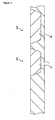
- Figure 1 is a sectional view showing an essential part of a semiconductor integrated circuit device according to Embodiment 1 of the present invention.
- an NMOS transistor 101 as a first MOS transistor, a PMOS transistor 201 as a second MOS transistor, and a triple-well NMOS transistor 301 as a third MOS transistor are formed on the same semiconductor substrate 1.
- the NMOS transistor 101 and the PMOS transistor 201 constitute a CMOS device.
- this semiconductor substrate 1 has other elements formed thereon in an element formed area partitioned by a field oxide film, but these elements are omitted from Figure 1 (this applies to the other figures).
- a first conductivity type corresponds to a P type and a second conductivity type corresponds to an N type, but vice versa (this applies to the other embodiments).
- the NMOS transistor 101 has a P-type well area (hereinafter referred to as a "P well area”) 2 formed on a main surface of a P-type semiconductor substrate (hereinafter referred to as a "P substrate") 1 and in an element formed area surrounded by a field oxide film 100 provided on the main surface of the P substrate 1.
- An N + source area 3, a P- channel formed area 4, and an N + drain area 5 are formed in the P well area 2 on the main surface of the P substrate 1.
- a gate electrode 7 is formed on the P - channel formed area 4 via a gate insulated film 6.
- the PMOS transistor 201 comprises an N-type well area (hereinafter referred to as an "N well area") formed on the main surface of the P substrate 1 and in the element formed area surrounded by the field oxide film 100 provided on the main surface of the P substrate 1.
- N well area an N-type well area
- a P + source area 13, an N - channel formed area 14, and a P + drain area 15 are formed in the N well area 18 and on the main surface of the P substrate 1.
- a gate electrode 17 is formed on the N- channel formed area 14 via a gate insulated film 16.
- the triple-well NMOS transistor 301 has an N well area 28 formed on the main surface of the P substrate 1 and in the element formed area surrounded by the field oxide film 100 provided on the main surface of the P substrate 1.
- a P well area 22 is formed in the N well area 28 and on the main surface of the P substrate 1.
- the P well area 22 has a surface concentration of about 0.75 x 10 17 to 1.25 to 10 17 /cm 3 .
- An N + source area 23, a P - channel formed area 24, and an N + drain area 25 are formed in the P well area 22 and on the main surface of the P substrate 1. Further, a gate electrode 27 is formed on the P - channel formed area 24 via a gate insulated film 26.
- the N + drain area 25 is located, for example, 0.5 ⁇ m or greater distance from the drain side end of the gate electrode 27.
- An impurity-diffused area 29 having a lower concentration of N-type impurities than the N + drain area 25 is formed between the drain side end of the gate electrode 27 and the N + drain area 25.
- the impurity-diffused area 29 has an xj of about 0.3 ⁇ m and a surface concentration of about 5 x 10 16 to 1 x 10 18 /cm 3 . Accordingly, the impurity-diffused area 29 functions as an N- offset drain area, which reduces electric fields at the drain side end of the gate electrode 27, thereby contributing to restraining the generation of hot electrons in an on state.
- a conductive portion, wires, a passivation film, and other parts constituting source and drain electrodes are laminated on the MOS transistors on the main surface of the P substrate 1 and on other elements (not shown).
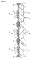
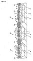
- Figures 2 and 3 are vertical sectional views showing essential parts of the semiconductor integrated circuit device according to Embodiment 1, which is in its manufacturing stage.
- the N well areas 18 and 28 are formed in the areas in which the PMOS transistor 201 and the triple-well NMOS transistor 301 are formed and on the main surface of the P substrate 1 by an ion injection method.
- the N well areas 18 and 28 can be formed in a single area without separating.
- the P well area 2 is formed in the area in which the NMOS transistor 101 is formed and on the main surface of the P substrate 1 by the ion injection method. Further, the P well area 22 is formed in the N well area 28 and on the main surface of the P substrate 1 by the ion injection method. At this time, the P well area 22 is formed simultaneously with the P well area 2. Subsequently, the field oxide film 100, the P-channel formed areas 4 and 24, the N- channel formed area 14, the gate insulated films 6, 16, and 26, and the gate electrodes 7, 17, and 27 are formed using a well-known method.
- the impurity diffusion area 29 as an N- offset drain area is formed only on the drain side of the gate electrode 27 by the ion injection method, on the basis of a self-alignment process that uses the gate electrode 27 as a mask, while using a mask (not shown) having a window pattern corresponding to the drain side portion of the triple-well NMOS transistor 301.
- This state is shown in Figure 3.
- the N + source areas 3 and 23 and the N + drain area 5 are formed by the ion injection method on the basis of the self-alignment process using the gate electrodes 7 and 27 as a mask.
- the N + drain area 25 is simultaneously formed using a mask (not shown) having a window pattern corresponding to the area of the triple-well NMOS transistor 301 in which the N + drain area 25 is formed. That is, the N + drain area 25 is not formed on the basis of the self-alignment process using the gate electrode 27 as a mask, but at the location defined by the mask.
- the P + source area 13 and the P + drain area 15 are formed by the ion injection method on the basis of a self-alignment process using the gate electrodes 17 as masks.
- the impurity-diffused areas including the area 29 are activated by thermal treatment. This state is shown in Figure 1.
- an interlayer insulated film is laminated all over the substrate, and contact holes are then opened therein. Then, a conductive portion, wires, a passivation film, and other parts constituting source and drain electrodes are formed to complete a semiconductor integrated circuit device.
- the impurity-diffused area 29, having a low concentration is formed in the triple-well NMOS transistor 301, so that electric fields at the drain side end of the gate electrode 27 are reduced to restrain the substrate current, which may lead to the flow of parasitic current from a parasitic bipolar transistor composed of the N + drain area 25, the P well area 22, and the N well area 28.
- substrate current can be reduced to about one-tenth to one-thousandth that in the NMOS transistor 101.
- the P well area 22 has a high impurity concentration, the current gain of the parasitic bipolar transistor decreases. Consequently, inappropriate operations caused by the malfunctioning of the parasitic bipolar transistor are prevented.
- FIG. 4 is a vertical sectional view showing an essential part of a semiconductor integrated circuit according to Embodiment 2 of the present invention.
- Embodiment 2 is the semiconductor integrated circuit device of Embodiment 1, to which LDD areas 31, 41, and 51 and spacer oxide films 32, 42, and 52 have been added. Since the other arrangements are the same as those of Embodiment 1, the same arrangements as those of Embodiment 1 are denoted by the same reference numerals, and the description thereof is omitted.
- the N- LDD areas 31 are formed between the source side end of the gate electrode 7 and the N + source area 3 and between the drain side end of the gate electrode 7 and the N + drain area 5.
- the N- LDD area 31 has a surface concentration of about 5 x 10 17 to 1 x 10 18 /cm 3 , which is lower than that of the source and drain areas 3 and 5.
- the spacer oxide film 32 is formed at the sides of the gate electrode 7.
- the P- LDD areas 41 are formed between the source side end of the gate electrode 17 and the P + source area 13 and between the drain side end of the gate electrode 17 and the P + drain area 15.
- the P-LDD area 41 has a surface concentration of about 5 x 10 17 to 1 x 10 18 /cm 3 , which is lower than that of the source and drain areas 13 and 15.
- the spacer oxide film 42 is formed at the sides of the gate electrode 17.
- the N-LDD area 51 is formed between the source side end of the gate electrode 27 and the N + source area 23.
- the N-LDD area 51 has a surface concentration of about 5 x 10 17 to 1 x 10 18 /cm 3 , which is lower than that of the source and drain areas 23 and 25.
- the spacer oxide film 52 is formed at the sides of the gate electrode 27.
- the impurity-diffused area 29 has a surface concentration of about 5 x 10 16 to 1 x 10 18 /cm 3
- it has a surface concentration of about 5 x 10 17 to 1 x 10 18 /cm 3 , which is the same as that of the N- LDD area 51.
- Figures 5 and 6 are vertical sectional views showing essential parts of the semiconductor integrated circuit device according to Embodiment 2, which is being manufactured by the first manufacture method.
- the N well areas 18 and 28, the P well areas 2 and 22, the field oxide film 100, the P - channel formed areas 4 and 24, the N - channel formed area 14, the gate insulated films 6, 16, and 26, and the gate electrodes 7, 17, and 27 are sequentially formed, as in the case with Embodiment 1.
- the N- LDD area 31 is formed by the ion injection method on the basis of a self-alignment process using the gate electrodes 7 of the NMOS transistor 111 as a mask.
- the N- LDD area 51 is formed close to the source side of the gate electrode 27 by the ion injection method on the basis of a self-alignment process using the gate electrodes 27 of the triple-well NMOS transistor 311 as a mask.
- the drain side of the gate electrode 27 is masked so that no impurities are injected into the drain side of the gate electrode 27.
- the P- LDD area 41 is formed by the ion injection method on the basis of a self-alignment process using the gate electrodes 17 as a mask. This state is shown in Figure 5.
- the impurity diffusion area 29 as an N - offset drain area is formed only on the drain side of the gate electrode 27 of the triple-well NMOS transistor 311 by the ion injection method. This state is shown in Figure 6.
- the spacer oxide films 32, 42, and 52 are formed.
- the N + source areas 3 and 23 and the N + drain area 5 are formed by the ion injection method on the basis of a self-alignment process using the spacer oxide films 32 and 52 as a mask.
- the N + drain area 25 is formed away from the gate electrode 27 using a mask (not shown) having a window pattern corresponding to the an area of the triple-well NMOS transistor 311 in which the N + drain area 25 is formed.
- the P + source area 13 and the P + drain area 15 are formed by the ion injection method on the basis of a self-alignment process using the spacer oxide film 42 as a mask.
- the impurity-diffused areas including the area 29 are activated by thermal treatment. This state is shown in Figure 4.
- Figure 7 is a vertical sectional view showing an essential part of the semiconductor integrated circuit device, which is being manufactured using the second manufacture method.
- the second manufacture method is the same as the first one, except for the step of forming the LDD areas 31, 41, and 51 and the subsequent steps.
- the impurity-diffused area 29 is also formed by injecting impurities into the drain side of the gate electrode 27. This eliminates the necessity of a mask for forming an offset drain area (impurity-diffused area 29) used in the above-described first manufacture method.
- This state is shown in Figure 7.
- the subsequent steps are the same as those of the above-described first manufacture method.
- the impurity-diffused area 29, having a low concentration is formed in the triple-well NMOS transistor 311, thereby reducing electric fields at the drain side end of the gate electrode 27. Consequently, as in the case with Embodiment 2, substrate current, which may lead to the flow of parasitic current from a parasitic bipolar transistor in the triple-well NMOS transistor 311, can be reduced to about one-tenth to one-thousandth that in the NMOS transistor 111. Further, since the P well area 22 has a high impurity concentration, the current gain of the parasitic bipolar transistor decreases. Therefore, inappropriate operations caused by the malfunctioning of the parasitic bipolar transistor are prevented.
- the impurity-diffused area 29 is formed together with the N - LDD areas 31 and 51, thereby reducing the number of masks used and thus the number of process steps to simplify the process.
- FIG 8 is a vertical sectional view showing an essential part of a semiconductor integrated circuit device according to Embodiment 3 of the present invention.
- Embodiment 3 is the semiconductor integrated circuit device of Embodiment 2 (see Figure 4), in which a P - punch-through stopper area 36 and an N - punch-through stopper area 46 are added to an NMOS transistor 121 as a first MOS transistor and a PMOS transistor 221 as a second MOS transistor, respectively, to restrain a punch-through phenomenon that may occur between the source areas 3 and 13 and the drain areas 5 and 15, respectively.
- the P - punch-through stopper area 36 has a higher impurity concentration than the P well area 2 and N well area 18.
- the NMOS transistor 121 and the PMOS transistor 221 constitute a submicron CMOS device having a channel length shorter than 1 ⁇ m. Since the other arrangements are the same as those of Embodiment 1 or 2, the same arrangements as those of Embodiment 1 or 2 are denoted by the same reference numerals, and the description thereof is omitted.
- the P - punch-through stopper area 36 and the N - punch-through stopper area 46 are formed by the ion injection method after the P well area 22 of the triple-well NMOS transistor 311 as a third MOS transistor has been formed and before the field oxide film 100 is formed. At this time, the triple-well NMOS transistor 311 is masked.
- This manufacture process is the same as that of Embodiment 2 except that the step of forming the punch-through stopper areas 36 and 46 is inserted in this manner. Consequently, the formation of the impurity-diffused area 29 may be carried out simultaneously with the formation of the N- LDD areas 31 and 51, or after it as a separate step.
- the substrate current can be reduced to about one-tenth to one-thousandth that in the NMOS transistor 121, and the current gain of the parasitic bipolar transistor decreases, thereby preventing inappropriate operations caused by the malfunctioning of the parasitic bipolar transistor, as in the case with Embodiment 2.
- the triple-well MOS transistor can be integrated on the same semiconductor substrate with a fine CMOS device.
- FIG. 9 is a vertical sectional view showing an essential part of a semiconductor integrated circuit device according to Embodiment 4 of the present invention.
- Embodiment 4 is the semiconductor integrated circuit device of Embodiment 3, in which the triple NMOS transistor 321 as a third MOS transistor also has a P - punch-through stopper area 56 formed therein, having depth of 1 ⁇ m.
- the P - punch-through stopper area 56 is formed together with the P - punch-through stopper area 36 of the NMOS transistor 121.
- the manufacture process is similar to that of Embodiment 3. Duplicate descriptions are omitted.
- the substrate current can be reduced to about one-tenth to one-thousandth that in the NMOS transistor 121, and the current gain of the parasitic bipolar transistor decreases, as with Embodiment 3. Furthermore, with the P - punch-through stopper area 56, the current gain of a parasitic bipolar transistor composed of the N + drain area 25, the P well area 22, the P - punch-through stopper area 56, and the N well area 28 can be reduced to 50 or less. Consequently, inappropriate operations caused by the malfunctioning of the parasitic bipolar transistor are prevented.
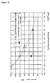
- the current gain is 50 when the P well area 22 has a surface concentration of 1 x 10 17 /cm 3 .
- the current gain is 140 when the P well area 22 has a surface concentration of 0.75 x 10 17 /cm 3 , 100 when the P well area 22 has a surface concentration of 1 x 10 17 /cm 3 , and 80 when the P well area 22 has a surface concentration of 1.25 x 10 17 /cm 3 .
- the P - punch-through stopper area 56 serves to compensate for an N-type semiconductor layer that may be formed on the surface of the P well area 22 of the triple-well NMOS transistor 321 after the formation of the P-well area 22.
- This N-type semiconductor layer is formed because the pile-up of phosphorous on the surface of the N well area 28 is facilitated by the consistent increase in the concentration of impurities in the N well area 28 with the miniaturisation of the transistor according to a scaling rule.
- a triple-well MOS transistor has a second-conductivity-type impurity-diffused area having a lower impurity concentration than a second-conductivity-type drain area, thereby restraining substrate current, which may lead to the flow of parasitic current from a parasitic bipolar transistor composed of a drain area, a first-conductivity-type well area, and a second-conductivity-type well area. Further, since the first-conductivity-type well area has a high impurity concentration, the current gain of the parasitic bipolar transistor decreases. Consequently, inappropriate operations caused by the malfunctioning of the parasitic bipolar transistor are prevented.
Landscapes
- Metal-Oxide And Bipolar Metal-Oxide Semiconductor Integrated Circuits (AREA)
Abstract
Description
Claims (9)
- A semiconductor integrated circuit device characterised by comprising:a first MOS transistor formed on a first-conductivity-type well area;a second MOS transistor formed on a second-conductivity-type well area; anda third MOS transistor formed on the first-conductivity-type well area that is formed within the second-conductivity-type well area, and having a second-conductivity-type drain area formed apart from a gate electrode end and a second-conductivity-type impurity-diffused area formed between said drain area and said gate electrode end, said second-conductivity-type impurity-diffused area having a lower impurity concentration than said drain area and connected to said drain area, and said first, second, and third MOS transistors being formed on the same semiconductor substrate.
- The semiconductor integrated circuit device according to Claim 1, characterised in that said third MOS transistor comprises a second-conductivity-type LDD area connected to a second-conductivity-type source area, and
said first MOS transistor and said second MOS transistor comprise a second-conductivity-type LDD area and a first-conductivity-type LDD area, respectively. - The semiconductor integrated circuit device according to Claim 2, characterised in that an impurity concentration of said impurity-diffused area is the same as that of said LDD areas of said third MOS transistor and said first MOS transistor.
- The semiconductor integrated circuit device according to any of Claims 1 to 3, characterised in that a punch-through stopper area that restrains occurrence of a punch-through phenomenon and has a higher impurity concentration than respective said first- and second-conductivity-type well areas is formed in each of said first-conductivity type well area having said first MOS transistor formed thereon and said second-conductivity-type well area having said second MOS transistor formed thereon.
- The semiconductor integrated circuit device according to any of Claims 1 to 4, characterised in that a first-conductivity-type diffused area is formed in said first-conductivity-type well area having said third MOS transistor formed therein.
- A method of manufacturing a semiconductor integrated circuit device consisting of a first MOS transistor formed on a first-conductivity-type well area, a second MOS transistor formed on a second-conductivity-type well area, and a third MOS transistor formed on the first-conductivity-type well area that is formed in the second-conductivity-type well area, said first, second, and third MOS transistors being formed on the same semiconductor substrate, the method being characterised by comprising steps of:simultaneously forming said second-conductivity-type well area of said second MOS transistor and said second-conductivity-type well area of said third MOS transistor on a main surface of said semiconductor substrate;forming said first-conductivity-type well area of said first MOS transistor on the main surface of said semiconductor substrate;forming said first-conductivity-type well area in said second-conductivity-type well area of said third MOS transistor and on the main surface of said semiconductor substrate;forming a gate insulated film and a gate electrode for each of said first MOS transistor, said second MOS transistor, and said third MOS transistor;forming an impurity-diffused area having a lower impurity concentration than a drain area, in said first-conductivity-type well area of said third MOS transistor and on the main surface of said semiconductor substrate, on the basis of a self-alignment process using said gate electrode as a mask;simultaneously forming a source area of said first MOS transistor, a drain area of said first MOS transistor, a source area of said third MOS transistor, and said drain area of said third MOS transistor formed apart from an end of said gate electrode and connected to said impurity-diffused area; andforming a source area and a drain area of said second MOS transistor.
- The method of manufacturing a semiconductor integrated circuit device according to Claim 6, characterised by further comprising a step of forming, in each of said first MOS transistor, said second MOS transistor, and said third MOS transistor, LDD areas on a source and a drain sides of said first MOS transistor, on a source and a drain sides of said second MOS transistor, and on a source side of said third MOS transistor, on the basis of a self-alignment process using said gate electrode as a mask, after said gate electrode has been formed and before said source area and said drain area are formed, the step being separate from formation of said impurity-diffused area.
- The method of manufacturing a semiconductor integrated circuit device according to Claim 6, characterised in that when said impurity-diffused area is formed, the LDD area is formed on each of the source and drain sides of said first MOS transistor and the source side of said third MOS transistor.
- The method of manufacturing a semiconductor integrated circuit device according to any of Claims 6 to 8, characterised in that said first-conductivity-type well area of said first MOS transistor and said first-conductivity-type well area of said third MOS transistor are simultaneously formed.
Applications Claiming Priority (2)
| Application Number | Priority Date | Filing Date | Title |
|---|---|---|---|
| JP2001015043A JP2002222869A (en) | 2001-01-23 | 2001-01-23 | Semiconductor integrated circuit device and method of manufacturing the same |
| JP2001015043 | 2001-01-23 |
Publications (3)
| Publication Number | Publication Date |
|---|---|
| EP1225627A2 true EP1225627A2 (en) | 2002-07-24 |
| EP1225627A3 EP1225627A3 (en) | 2005-01-12 |
| EP1225627B1 EP1225627B1 (en) | 2009-06-10 |
Family
ID=18881659
Family Applications (1)
| Application Number | Title | Priority Date | Filing Date |
|---|---|---|---|
| EP02250303A Expired - Lifetime EP1225627B1 (en) | 2001-01-23 | 2002-01-16 | Semiconductor integrated circuit device and manufacture method therefor |
Country Status (4)
| Country | Link |
|---|---|
| US (2) | US6809376B2 (en) |
| EP (1) | EP1225627B1 (en) |
| JP (1) | JP2002222869A (en) |
| DE (1) | DE60232563D1 (en) |
Families Citing this family (4)
| Publication number | Priority date | Publication date | Assignee | Title |
|---|---|---|---|---|
| TWI256724B (en) * | 2003-08-06 | 2006-06-11 | Sanyo Electric Co | Semiconductor device |
| JP4664631B2 (en) * | 2004-08-05 | 2011-04-06 | 株式会社東芝 | Semiconductor device and manufacturing method thereof |
| US7800428B2 (en) * | 2006-11-03 | 2010-09-21 | Infineon Technologies Ag | Semiconductor device and method for controlling a semiconductor device |
| KR102684973B1 (en) * | 2018-10-10 | 2024-07-17 | 삼성전자주식회사 | Latch circuit |
Family Cites Families (14)
| Publication number | Priority date | Publication date | Assignee | Title |
|---|---|---|---|---|
| US5030585A (en) * | 1990-03-22 | 1991-07-09 | Micron Technology, Inc. | Split-polysilicon CMOS DRAM process incorporating selective self-aligned silicidation of conductive regions and nitride blanket protection of N-channel regions during P-channel gate spacer formation |
| JP2545762B2 (en) * | 1990-04-13 | 1996-10-23 | 日本電装株式会社 | High breakdown voltage MIS transistor and method of manufacturing complementary transistor having this transistor |
| JP3002371B2 (en) * | 1993-11-22 | 2000-01-24 | 富士通株式会社 | Semiconductor device and manufacturing method thereof |
| JPH07183390A (en) | 1993-12-24 | 1995-07-21 | Oki Electric Ind Co Ltd | Cmis semiconductor device and fabrication thereof |
| JPH07263680A (en) * | 1994-03-24 | 1995-10-13 | Hitachi Ltd | Method for manufacturing semiconductor device |
| US5675168A (en) * | 1994-04-01 | 1997-10-07 | Matsushita Electric Industrial Co., Ltd. | Unsymmetrical MOS device having a gate insulator area offset from the source and drain areas, and ESD protection circuit including such a MOS device |
| JP3601612B2 (en) * | 1994-09-22 | 2004-12-15 | 富士通株式会社 | Semiconductor device and manufacturing method thereof |
| JPH09246478A (en) * | 1996-03-01 | 1997-09-19 | Hitachi Ltd | Semiconductor integrated circuit device and method of manufacturing the same |
| JP3777000B2 (en) * | 1996-12-20 | 2006-05-24 | 富士通株式会社 | Semiconductor device and manufacturing method thereof |
| JPH10223892A (en) * | 1997-02-04 | 1998-08-21 | Toshiba Microelectron Corp | Semiconductor device and manufacturing method thereof |
| JP3315356B2 (en) * | 1997-10-15 | 2002-08-19 | 株式会社東芝 | High voltage semiconductor device |
| JPH11233769A (en) | 1998-02-12 | 1999-08-27 | Semiconductor Energy Lab Co Ltd | Semiconductor device and manufacturing method thereof |
| JP2000091574A (en) | 1998-09-07 | 2000-03-31 | Denso Corp | Semiconductor device and method of manufacturing semiconductor device |
| JP3536693B2 (en) * | 1998-11-24 | 2004-06-14 | セイコーエプソン株式会社 | Semiconductor storage device and method of manufacturing the same |
-
2001
- 2001-01-23 JP JP2001015043A patent/JP2002222869A/en active Pending
-
2002
- 2002-01-16 EP EP02250303A patent/EP1225627B1/en not_active Expired - Lifetime
- 2002-01-16 DE DE60232563T patent/DE60232563D1/en not_active Expired - Lifetime
- 2002-01-23 US US10/055,717 patent/US6809376B2/en not_active Expired - Fee Related
-
2003
- 2003-05-12 US US10/435,956 patent/US20030207509A1/en not_active Abandoned
Also Published As
| Publication number | Publication date |
|---|---|
| JP2002222869A (en) | 2002-08-09 |
| EP1225627B1 (en) | 2009-06-10 |
| US20020117713A1 (en) | 2002-08-29 |
| DE60232563D1 (en) | 2009-07-23 |
| US20030207509A1 (en) | 2003-11-06 |
| US6809376B2 (en) | 2004-10-26 |
| EP1225627A3 (en) | 2005-01-12 |
Similar Documents
| Publication | Publication Date | Title |
|---|---|---|
| KR100392901B1 (en) | Method of manufacturing an asymmetric slightly doped drain (LCD) MOS device | |
| US10032903B2 (en) | Threshold voltage adjustment of a transistor | |
| US7544573B2 (en) | Semiconductor device including MOS field effect transistor having offset spacers or gate sidewall films on either side of gate electrode and method of manufacturing the same | |
| JPH01205470A (en) | Semiconductor device and its manufacture | |
| JPH0730107A (en) | High voltage transistor and method of manufacturing the same | |
| EP0091256B1 (en) | Cmos device | |
| US6476430B1 (en) | Integrated circuit | |
| JP2001284540A (en) | Semiconductor device and method of manufacturing the same | |
| US7138311B2 (en) | Semiconductor integrated circuit device and manufacture method therefore | |
| US5610427A (en) | Electrostatic protection device for use in semiconductor integrated circuit | |
| EP1225627B1 (en) | Semiconductor integrated circuit device and manufacture method therefor | |
| JP3252790B2 (en) | Semiconductor integrated circuit | |
| JPH10135349A (en) | CMOS semiconductor device and method of manufacturing the same | |
| US7642617B2 (en) | Integrated circuit with depletion mode JFET | |
| US5550064A (en) | Method for fabricating high-voltage complementary metal-oxide-semiconductor transistors | |
| US5858827A (en) | Method of manufacturing MOS transistor device with improved threshold value control and reduced reverse short channel effect | |
| JPH08306799A (en) | Input protection circuit and method for manufacturing semiconductor integrated circuit device | |
| JP2743828B2 (en) | Semiconductor device and manufacturing method thereof | |
| US5850360A (en) | High-voltage N-channel MOS transistor and associated manufacturing process | |
| JP3970689B2 (en) | Semiconductor device and manufacturing method thereof | |
| JP2507981B2 (en) | Manufacturing method of complementary MIS transistor | |
| JPH07254645A (en) | Method for manufacturing semiconductor device | |
| JP4068671B2 (en) | Manufacturing method of semiconductor integrated circuit device | |
| JPH1032262A (en) | Method for manufacturing CMOS device | |
| JPH1117022A (en) | Electrostatic breakdown protection element and method of manufacturing the same |
Legal Events
| Date | Code | Title | Description |
|---|---|---|---|
| PUAI | Public reference made under article 153(3) epc to a published international application that has entered the european phase |
Free format text: ORIGINAL CODE: 0009012 |
|
| AK | Designated contracting states |
Kind code of ref document: A2 Designated state(s): AT BE CH CY DE DK ES FI FR GB GR IE IT LI LU MC NL PT SE TR |
|
| AX | Request for extension of the european patent |
Free format text: AL;LT;LV;MK;RO;SI |
|
| PUAL | Search report despatched |
Free format text: ORIGINAL CODE: 0009013 |
|
| AK | Designated contracting states |
Kind code of ref document: A3 Designated state(s): AT BE CH CY DE DK ES FI FR GB GR IE IT LI LU MC NL PT SE TR |
|
| AX | Request for extension of the european patent |
Extension state: AL LT LV MK RO SI |
|
| 17P | Request for examination filed |
Effective date: 20050531 |
|
| AKX | Designation fees paid |
Designated state(s): DE IT NL |
|
| 17Q | First examination report despatched |
Effective date: 20060515 |
|
| GRAP | Despatch of communication of intention to grant a patent |
Free format text: ORIGINAL CODE: EPIDOSNIGR1 |
|
| GRAS | Grant fee paid |
Free format text: ORIGINAL CODE: EPIDOSNIGR3 |
|
| GRAA | (expected) grant |
Free format text: ORIGINAL CODE: 0009210 |
|
| AK | Designated contracting states |
Kind code of ref document: B1 Designated state(s): DE IT NL |
|
| REF | Corresponds to: |
Ref document number: 60232563 Country of ref document: DE Date of ref document: 20090723 Kind code of ref document: P |
|
| NLV1 | Nl: lapsed or annulled due to failure to fulfill the requirements of art. 29p and 29m of the patents act | ||
| PG25 | Lapsed in a contracting state [announced via postgrant information from national office to epo] |
Ref country code: NL Free format text: LAPSE BECAUSE OF FAILURE TO SUBMIT A TRANSLATION OF THE DESCRIPTION OR TO PAY THE FEE WITHIN THE PRESCRIBED TIME-LIMIT Effective date: 20090610 |
|
| PLBE | No opposition filed within time limit |
Free format text: ORIGINAL CODE: 0009261 |
|
| STAA | Information on the status of an ep patent application or granted ep patent |
Free format text: STATUS: NO OPPOSITION FILED WITHIN TIME LIMIT |
|
| 26N | No opposition filed |
Effective date: 20100311 |
|
| PG25 | Lapsed in a contracting state [announced via postgrant information from national office to epo] |
Ref country code: IT Free format text: LAPSE BECAUSE OF FAILURE TO SUBMIT A TRANSLATION OF THE DESCRIPTION OR TO PAY THE FEE WITHIN THE PRESCRIBED TIME-LIMIT Effective date: 20090610 |
|
| REG | Reference to a national code |
Ref country code: DE Ref legal event code: R082 Ref document number: 60232563 Country of ref document: DE Representative=s name: PATENTANWAELTE CHARRIER RAPP & LIEBAU, DE Effective date: 20110826 Ref country code: DE Ref legal event code: R081 Ref document number: 60232563 Country of ref document: DE Owner name: FUJI ELECTRIC CO., LTD., JP Free format text: FORMER OWNER: FUJI ELECTRIC SYSTEMS CO., LTD., TOKYO/TOKIO, JP Effective date: 20110826 Ref country code: DE Ref legal event code: R081 Ref document number: 60232563 Country of ref document: DE Owner name: FUJI ELECTRIC CO., LTD., KAWASAKI-SHI, JP Free format text: FORMER OWNER: FUJI ELECTRIC SYSTEMS CO., LTD., TOKYO/TOKIO, JP Effective date: 20110826 |
|
| REG | Reference to a national code |
Ref country code: DE Ref legal event code: R084 Ref document number: 60232563 Country of ref document: DE |
|
| REG | Reference to a national code |
Ref country code: DE Ref legal event code: R084 Ref document number: 60232563 Country of ref document: DE Effective date: 20120521 |
|
| PGFP | Annual fee paid to national office [announced via postgrant information from national office to epo] |
Ref country code: DE Payment date: 20150113 Year of fee payment: 14 |
|
| REG | Reference to a national code |
Ref country code: DE Ref legal event code: R119 Ref document number: 60232563 Country of ref document: DE |
|
| PG25 | Lapsed in a contracting state [announced via postgrant information from national office to epo] |
Ref country code: DE Free format text: LAPSE BECAUSE OF NON-PAYMENT OF DUE FEES Effective date: 20160802 |