EP1223609A1 - Polishing compound for chemimechanical polishing and polishing method - Google Patents
Polishing compound for chemimechanical polishing and polishing method Download PDFInfo
- Publication number
- EP1223609A1 EP1223609A1 EP00955039A EP00955039A EP1223609A1 EP 1223609 A1 EP1223609 A1 EP 1223609A1 EP 00955039 A EP00955039 A EP 00955039A EP 00955039 A EP00955039 A EP 00955039A EP 1223609 A1 EP1223609 A1 EP 1223609A1
- Authority
- EP
- European Patent Office
- Prior art keywords
- polishing
- acid
- film
- cmp
- water
- Prior art date
- Legal status (The legal status is an assumption and is not a legal conclusion. Google has not performed a legal analysis and makes no representation as to the accuracy of the status listed.)
- Withdrawn
Links
Images
Classifications
-
- C—CHEMISTRY; METALLURGY
- C09—DYES; PAINTS; POLISHES; NATURAL RESINS; ADHESIVES; COMPOSITIONS NOT OTHERWISE PROVIDED FOR; APPLICATIONS OF MATERIALS NOT OTHERWISE PROVIDED FOR
- C09K—MATERIALS FOR MISCELLANEOUS APPLICATIONS, NOT PROVIDED FOR ELSEWHERE
- C09K3/00—Materials not provided for elsewhere
- C09K3/14—Anti-slip materials; Abrasives
- C09K3/1454—Abrasive powders, suspensions and pastes for polishing
- C09K3/1463—Aqueous liquid suspensions
-
- B—PERFORMING OPERATIONS; TRANSPORTING
- B24—GRINDING; POLISHING
- B24B—MACHINES, DEVICES, OR PROCESSES FOR GRINDING OR POLISHING; DRESSING OR CONDITIONING OF ABRADING SURFACES; FEEDING OF GRINDING, POLISHING, OR LAPPING AGENTS
- B24B37/00—Lapping machines or devices; Accessories
- B24B37/11—Lapping tools
- B24B37/20—Lapping pads for working plane surfaces
- B24B37/24—Lapping pads for working plane surfaces characterised by the composition or properties of the pad materials
-
- B—PERFORMING OPERATIONS; TRANSPORTING
- B24—GRINDING; POLISHING
- B24B—MACHINES, DEVICES, OR PROCESSES FOR GRINDING OR POLISHING; DRESSING OR CONDITIONING OF ABRADING SURFACES; FEEDING OF GRINDING, POLISHING, OR LAPPING AGENTS
- B24B37/00—Lapping machines or devices; Accessories
- B24B37/04—Lapping machines or devices; Accessories designed for working plane surfaces
- B24B37/042—Lapping machines or devices; Accessories designed for working plane surfaces operating processes therefor
- B24B37/044—Lapping machines or devices; Accessories designed for working plane surfaces operating processes therefor characterised by the composition of the lapping agent
-
- C—CHEMISTRY; METALLURGY
- C09—DYES; PAINTS; POLISHES; NATURAL RESINS; ADHESIVES; COMPOSITIONS NOT OTHERWISE PROVIDED FOR; APPLICATIONS OF MATERIALS NOT OTHERWISE PROVIDED FOR
- C09G—POLISHING COMPOSITIONS; SKI WAXES
- C09G1/00—Polishing compositions
- C09G1/02—Polishing compositions containing abrasives or grinding agents
-
- C—CHEMISTRY; METALLURGY
- C09—DYES; PAINTS; POLISHES; NATURAL RESINS; ADHESIVES; COMPOSITIONS NOT OTHERWISE PROVIDED FOR; APPLICATIONS OF MATERIALS NOT OTHERWISE PROVIDED FOR
- C09G—POLISHING COMPOSITIONS; SKI WAXES
- C09G1/00—Polishing compositions
- C09G1/04—Aqueous dispersions
-
- H—ELECTRICITY
- H10—SEMICONDUCTOR DEVICES; ELECTRIC SOLID-STATE DEVICES NOT OTHERWISE PROVIDED FOR
- H10P—GENERIC PROCESSES OR APPARATUS FOR THE MANUFACTURE OR TREATMENT OF DEVICES COVERED BY CLASS H10
- H10P52/00—Grinding, lapping or polishing of wafers, substrates or parts of devices
- H10P52/40—Chemomechanical polishing [CMP]
- H10P52/403—Chemomechanical polishing [CMP] of conductive or resistive materials
-
- C—CHEMISTRY; METALLURGY
- C11—ANIMAL OR VEGETABLE OILS, FATS, FATTY SUBSTANCES OR WAXES; FATTY ACIDS THEREFROM; DETERGENTS; CANDLES
- C11D—DETERGENT COMPOSITIONS; USE OF SINGLE SUBSTANCES AS DETERGENTS; SOAP OR SOAP-MAKING; RESIN SOAPS; RECOVERY OF GLYCEROL
- C11D2111/00—Cleaning compositions characterised by the objects to be cleaned; Cleaning compositions characterised by non-standard cleaning or washing processes
- C11D2111/10—Objects to be cleaned
- C11D2111/14—Hard surfaces
- C11D2111/22—Electronic devices, e.g. PCBs or semiconductors
Definitions
- This invention relates to a polishing medium for chemical-mechanical polishing, especially suited for polishing in the step of forming wirings of semiconductor devices, and a polishing method making use of the same.
- CMP chemical-mechanical polishing
- polishing pad is fastened onto a circular polishing roller (platen), and the surface of the polishing pad is soaked with a polishing medium for chemical-mechanical polishing, where a substrate with a metal film formed thereon is pressed against the pad on the former's metal film side and a stated pressure (hereinafter “polishing pressure”) is applied thereto on the back thereof, in the state of which the polishing platen is turned to remove the metal film at the part of its hills by mechanical friction acting between the polishing medium and the metal film.
- polishing pressure a stated pressure
- the polishing medium used in such CMP is commonly comprised of an oxidizing agent and solid abrasive grains, to which a metal-oxide-dissolving agent and/or a protective-film-forming agent are optionally added.
- the basic mechanism of CMP making use of this polishing medium for CMP is considered to be that the metal film surface is oxidized with the oxidizing agent and the resultant oxide layer is scraped with the solid abrasive grains.
- the metal surface oxide layer at the part of dales does not come into contact with the polishing pad so much and the effect of scraping attributable to the solid abrasive grains does not extend thereto.
- the metal layer becomes removed at its hills and the substrate (with film) surface become flat. Details on this matter are disclosed in Journal of Electrochemical Society, Vol. 138, No. 11 (published 1991), pages 3460-3464.
- the metal-oxide-dissolving agent makes the metal film surface oxide layer dissolve (hereinafter "etching") also at the part of dales, and the metal film surface becomes uncovered, so that the metal film surface is further oxidized by the oxidizing agent. With repetition of this, the etching of the metal film may proceed at the part of dales, resulting in a damage of the effect of flattening.
- the protective-film-forming agent is further added to the metal-polishing medium for CMP.
- adding the metal-oxide-dissolving agent and protective-film-forming agent adds the effect of chemical reaction, and this brings about the effect that the CMP rate (the rate of polishing by CMP) is improved and also any injury (damage) of the metal layer surface to be polished by CMP may less occur.
- polishing medium which does not etch the metal film surface oxide layer so much at the part of dales, dissolves in a good efficiency the particles of the oxide layer scraped off, and has a high rate of polishing.
- a polishing method making use of a polishing medium for CMP which contains a metal-oxide-dissolving agent comprised of amino acetic acid (e.g., glycine) or amidosulfuric acid and contains BTA (benzotriazole) is proposed.
- a metal-oxide-dissolving agent comprised of amino acetic acid (e.g., glycine) or amidosulfuric acid and contains BTA (benzotriazole)
- the BTA has a very high protective-film-forming effect, and hence it may greatly lower not only the rate of etching but also the rate of polishing. Accordingly, it is sought to provide a polishing medium for CMP which lowers the etching rate sufficiently but does not lower the CMP rate.
- An object of the present invention is to provide a polishing medium for CMP and a polishing method which can form highly reliable buried metal film patterns in a good efficiency by making the etching rate sufficiently low while keeping a high CMP rate.
- the protective-film-forming agent a compound by which a chelate complex is readily formed with copper is used, such as ethylenediaminetetraacetic acid or benzotriazole. Such a compound has a very strong effect of forming a protective film on the surface to be polished.
- the copper alloy film comes not subject to CMP, to say nothing of etching.
- the present inventors have discovered that the use of the protective-film-forming agent in combination with a water-soluble polymer enables achievement of a high CMP rate while keeping a sufficiently low etching rate. They have moreover discovered that the use of such a polishing medium enables the polishing to be carried out at a practical CMP rate even without incorporating any solid abrasive grains in the polishing medium.
- the water-soluble polymer is added to a metal polishing medium containing an oxidizing agent for the polishing object, a metal-oxide-dissolving agent, a protective-film-forming agent and water, whereby the CMP rate can be made higher while the etching rate is kept low.
- etching rate As to the value of etching rate, it has been found that a preferable flattening effect can be achieved as long as the etching rate is controlled to 10 nm/minute or less. As long as the lowering of CMP rate is within a tolerable range, it is desirable for the etching rate to be much lower. As long as the etching rate is controlled to 5 nm/minute or less, the dishing can be kept to a degree not coming into question even when, e.g., the CMP is performed in excess by about 50% (i.e., CMP is performed for a time 1.5 times that necessary for removing the polishing object) . As long as the etching rate can further be controlled to 1 nm/minute or less, the dishing does not come into question even when the CMP is performed in excess by about 100% or more.
- the present invention provides a polishing medium for CMP, comprising an oxidizing agent, a metal-oxide-dissolving agent, a protective-film-forming agent, a water-soluble polymer, and water, and a polishing method making use of this polishing medium.
- the polishing medium for CMP may preferably satisfy at least one of the following (1) to (4), and may particularly preferably satisfy all of them.
- That the water-soluble polymer has a weight-average molecular weight of 500 or more.
- the water-soluble polymer may preferably have a weight-average molecular weight of 500 or more, more preferably 1,500 or more, and particularly preferably 5,000 or more.
- the upper limit of the weight-average molecular weight is not particularly defined. From the viewpoint of solubility, it may preferably be 5,000,000 or less.
- water-soluble polymer two or more polymers each having a weight-average molecular weight of 500 or more but a weight-average molecular weight different from each other may preferably be used in combination, which may be water-soluble polymers of the same type or may be water-soluble polymers of different types.
- the weight-average molecular weight is determined by measurement on a GPC (gel permeation chromatography) column through which an aqueous solution of the water-soluble polymer is flowed.
- That the polishing medium has a coefficient of kinetic friction of 0.25 or more.
- the CMP rate can be made much higher while the etching rate is kept low.
- a higher CMP rate can be achieved as a higher coefficient of kinetic friction the metal polishing medium used has.
- the coefficient of kinetic friction is a coefficient obtained where the force applied to a wafer carrier when the metal film on the surface of a wafer is polished, i.e., kinetic frictional force, is divided by polishing pressure. Stated specifically, it is determined by calculation from measurements of tensile stress or the like.
- the polishing medium for CMP of the present invention may more preferably have a coefficient of kinetic friction of 0.35 or more, and particularly preferably 0.45 or more.
- That the polishing medium has a viscosity by Ubbelode viscometer (hereinafter “Ubbelode's viscosity”) of from 0.95 cP to 1.5 cP.
- Ubbelode's viscosity a viscosity by Ubbelode viscometer
- the CMP rate can be made much higher while the etching rate is kept low.
- a higher CMP rate can be achieved as a higher Ubbelode's viscosity the metal polishing medium used has.
- the Ubbelode's viscosity is the value obtained where the time in which the polishing medium for CMP, kept at a liquid temperature of 25°C in a glass tube for measuring Ubbelode's viscosity, moves over a specified distance is measured and the resultant movement time is multiplied by a constant (JIS K2283) .
- the polishing medium may more preferably have a Ubbelode's viscosity of from 0.96 to 1.3 cP, and particularly preferably from 0.97 to 1.0 cP.
- That the polishing medium has a point-of-inflection pressure of 50 gf/cm 2 or more.
- the polishing medium has a point-of-inflection pressure of 50 gf/cm 2 or more, the effect of achieving high flattening, low dishing level and low erosion level can more effectively be brought out.
- the point-of-inflection pressure refers to the polishing pressure at which the CMP rate rises abruptly. Stated specifically, it is the polishing pressure (intermediate value) in a region where the CMP rate increases from 10 nm/minute or less to 50 nm/minute or more, and is determined by measuring the rate of polishing (CMP rate) under various polishing pressure.
- the polishing medium may preferably have a point-of-inflection pressure of 50 gf/cm 2 or more, and more preferably 100 gf/cm 2 or more. If its point-of-inflection pressure is less than 50 gf/cm 2 , the effect of high flattening tends to be less brought out.
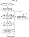
- Fig. 1 is an illustration showing the steps of polishing a substrate member in Examples.
- composition of polishing medium A. Composition of polishing medium:
- the polishing medium for CMP of the present invention comprises an oxidizing agent, a metal-oxide-dissolving agent, a protective-film-forming agent, a water-soluble polymer, and water.
- the respective components are described below.
- the oxidizing agent to be contained in the polishing medium for CMP of the present invention is a compound having oxidizing power on the polishing object. Stated specifically, it may include hydrogen peroxide, nitric acid, potassium periodate, hypochlorous acid and ozone water. Of these, hydrogen peroxide is particularly preferred. Any one compound of these may be used alone, or two or more compounds may be used in combination.
- the substrate member is a silicon substrate member including devices for integrated circuits
- the oxidizing agent it is undesirable for it to be contaminated with alkali metals, alkaline earth metals, halides and so forth.
- the oxidizing agent it is preferable for the oxidizing agent not to contain any involatile component.
- the ozone water may undergo a great compositional change with time.
- the hydrogen peroxide is most suited for the present invention.
- the substrate member to be polished is a glass substrate member not including any semiconductor devices
- an oxidizing agent containing an involatile component may be used without any problem.
- the oxidizing agent component may preferably be mixed in an amount of from 0.003 mol to 0.7 mol, more preferably from 0.03 mol to 0.5 mol, and particularly preferably from 0.2 mol to 0.3 mol, baseed on the total weight 100 g of the oxidizing agent, metal-oxide-dissolving agent, protective-film-forming agent, water-soluble polymer and water. If it is mixed in an amount of less than 0.003 mol, the metal may insufficiently be oxidized. If it is more than 0.7 mol, the polishing surface tends to be roughed.
- the metal-oxide-dissolving agent to be contained in the polishing medium for CMP of the present invention at least one of an organic acid, an organic-acid ester, an organic-acid ammonium salt and sulfuric acid is preferred.
- the metal-oxide-dissolving agent may preferably be water-soluble, and may also be mixed in the state of an aqueous solution.
- metal-oxide-dissolving agents preferable for the present invention they may include organic acids such as formic acid, acetic acid, propionic acid, butyric acid, valeric acid, 2-methylbutyric acid, n-hexanoic acid, 3,3-dimethylbutyric acid, 2-ethylbutyric acid, 4-methylpentanoic acid, n-heptanoic acid, 2-methylhexanoic acid, n-octanoic acid, 2-ethylhexanoic acid, benzoic acid, glycolic acid, salicylic acid, glyceric acid, oxalic acid, malonic acid, succinic acid, glutaric acid, adipic acid, pimelic acid, maleic acid, phthalic acid, malic acid, tartaric acid and citric acid; esters of these organic acids
- the polishing medium for CMP which makes use of any of these is suited for layered films having conductor (which may also be semiconductor) layers formed of copper, a copper alloy, a copper oxide and/or a copper alloy oxide (hereinafter these are generically termed "copper alloy" in some cases) .
- conductor which may also be semiconductor
- copper alloy copper alloy oxide
- malic acid, tartaric acid and citric acid are preferred in view of an advantage that the etching rate can effectively be controlled while practical CMP polishing rate is maintained.
- the metal-oxide-dissolving agent component in the present invention may preferably be mixed in an amount of from 0 mol to 0.005 mol, more preferably from 0.00005 mol to 0.0025 mol, and particularly preferably from 0.0005 mol to 0.0015 mol, baseed on the total weight 100 g of the oxidizing agent, metal-oxide-dissolving agent, protective-film-forming agent, water-soluble polymer and water. If it is mixed in an amount of more than 0.005 mol, the etching tends to be controlled with difficulty.
- the protective-film-forming agent is a compound which forms a protective film on the surface of the polishing object, and nitrogen-containing compounds (e.g., ammonia, alkylamines, amino acids, imines, azoles, and salts of these), mercaptans, glucose and cellulose are preferred.
- nitrogen-containing compounds e.g., ammonia, alkylamines, amino acids, imines, azoles, and salts of these
- mercaptans e.g., glucose and cellulose are preferred.
- protective-film-forming agents may include ammonia; alkylamines such as dimethylamine, trimethylamine, triethylamine, propylenediamine, ethylenediaminetetraacetic acid (EDTA), sodium diethyldithiocarbamate and chitosan; amino acids such as glycine, L-alanine, ⁇ -alanine, L-2-aminobuyric acid, L-norvaline, L-valine, L-leucine, L-norleucine, L-isoleucine, L-alloisoleucine, L-phenylalanine, L-proline, sarcocine, L-ornithine, L-lysine, taurine, L-serine, L-threonine, L-allothreonine, L-homoserine, L-tyrosine, 3,5-diiodo-L-tyrosine, ⁇ -(3,4
- chitosan ethylenediaminetetraacetic acid, L-tryptophane, cuperazone, triazinedithiol, benzotriazole, 4-hydroxybenzotriazole, 4-carboxyl-1H-benzotriazole butyl ester, tolyltriazole and naphthotriazole are preferred in order to achieve both a high CMP rate and a low etching rate.
- the protective-film-forming agent may be mixed in an amount of from 0.0001 mol to 0.05 mol, more preferably from 0.0003 mol to 0.005 mol, and particularly preferably from 0.0005 mol to 0.0035 mol, baseed on the total weight 100 g of the oxidizing agent, metal-oxide-dissolving agent, protective-film-forming agent, water-soluble polymer and water. If it is mixed in an amount of less than 0.0001 mol, the etching tends to be controlled low with difficulty. If it is in an amount of more than 0.05 mol, a low CMP rate tends to result.
- water-soluble polymers may include polysaccharides such as alginic acid, pectic acid, carboxymethylcellulose, agar, curdlan and pullulan; polycarboxylic acids such as polyaspertic acid, polyglutamic acid, polylysine, polymalic acid, polymethacrylic acid, ammonium polymethacrylate, sodium polymethacrylate, polyamic acid, polymaleic acid, polyitaconic acid, polyfumaric acid, poly(p-styrenecarboxylic acid), polyacrylic acid, polyacrylamide, aminopolyacrylamide, methyl polyacrylate, ethyl polyacrylate, ammonium polyacrylate, sodium polyacrylate, polyamic acid, polyamic acid ammonium salt and polyamic acid sodium salt and polyglyoxylic acid, polycarboxylic esters, and salts thereof; and vinyl polymers such as polyvinyl alcohol, polyvinyl pyrrolidone and polyacrolein.
- polysaccharides such
- the substrate member to be polished is a silicon substrate member for semiconductor integrated circuits, acids or ammonium salts are preferred because it is undesirable for it to be contaminated with alkali metals, alkaline earth metals, halides and so forth. Where the substrate member is a glass substrate member, this does not necessarily apply.
- pectic acid pectic acid, agar, polymalic acid, polymethacrylic acid, polyacrylic acid, polyacrylamide, polyvinyl alcohol and polyvinyl pyrrolidone, esters of these and ammonium salts of these are particularly preferred.
- the water-soluble polymer may be mixed in an amount of from 0.001 to 0.3% by weight, more preferably from 0.003 to 0.1% by weight, and particularly preferably from 0.01 to 0.08% by weight, baseed on the total weight 100 g of the oxidizing agent, metal-oxide-dissolving agent, protective-film-forming agent, water-soluble polymer and water. If it is mixed in an amount of less than 0.001% by weight, the effect attributable to its use in combination with the protective-film-forming agent tends not to be brought out in low etching control. If it is in an amount of more than 0.3% by weight, a low CMP rate tends to result.
- the polishing medium for CMP of the present invention may optionally appropriately contain additives.
- the solid abrasive grains need not substantially be contained, or may be contained. Also, in the case of the polishing medium for CMP of the present invention which does not contain any abrasive grains, the CMP proceeds by the action of the friction with a polishing pad which is mechanically much softer than the solid abrasive grains, and hence the polishing defects can be made to dramatically less occur.
- the polishing medium of the present invention can flatten polishing objects by CMP without relying on any strong mechanical friction caused by solid abrasive grains, but by the action of the friction with the polishing pad which is much softer than them.
- the protective-film-forming agent is used in combination with the water-soluble polymer, the etching is controlled but, in the friction with the polishing pad, the protective-film-forming agent does not function and the CMP proceeds, as so presumed.
- the degree at which the polishing mars occur depends on the particle diameter, particle size distribution and shape of the solid abrasive grains.
- the decrease in layer thickness (hereinafter “erosion”) due to the scrape of insulating film and the deterioration of flattening effect also depends on the particle diameter of the solid abrasive grains and the physical properties of the polishing pad.
- the dishing of the metal film is considered to depend on the hardness of the polishing pad and the chemical properties of the polishing medium. More specifically, hard solid abrasive grains are necessary for the progress of CMP, but are undesirable for the improvement of flattening effect in CMP and perfectness (free of any damage such as polishing mars) of CMP surface. From this fact, it is seen that in fact the flattening effect depends on the properties of the polishing pad which is softer than the solid abrasive grains.
- the polishing medium for CMP of the present invention is very favorable for the CMP of copper alloys and furthermore the formation of buried patterns making use of the same.
- the present invention provides a polishing method comprising polishing a polishing object film of a metal or metal oxide by the use of the above polishing medium for CMP of the present invention to remove at least part of the polishing object film.
- the polishing medium for CMP of the present invention can achieve high flattening at a high speed, even when the polishing object film is a layered film comprised of copper, a copper alloy, a copper oxide and/or a copper alloy oxide.
- the polishing method of the present invention can polish the polishing object film by feeding the polishing medium for CMP of the present invention to a polishing cloth on a polishing platen, and simultaneously bringing a substrate having the polishing object film thereon, into contact with the polishing cloth, in the state of which the polishing platen and the substrate (with film) are relatively moved.
- a metal film comprised of copper or a copper alloy (such as copper/chromium) is formed on a substrate having dales at its surface, filling the dales with the metal film.
- This substrate member is subjected to CMP using the polishing medium according to the present invention, whereupon the metal film at the part of hills of the substrate member is selectively polished away by CMP and the metal film at the part of dales is left therein, thus the desired conductor pattern is obtained.
- a commonly available polishing apparatus which has a holder for holding the polishing object such as a semiconductor substrate member and a platen to which a polishing cloth (pad) has been fastened (fitted with, e.g., a motor whose number of revolutions is variable).
- a polishing cloth commonly available nonwoven fabric, foamed polyurethane, porous fluorine resin and so forth may be used without any particular limitations.
- polishing conditions There are no particular limitations on polishing conditions. It is preferable to rotate the platen at a low revolution of 200 rpm or less so that the substrate does not rush out therefrom.
- the semiconductor substrate member having the polishing object film may preferably be pressed against the polishing cloth at a pressure of from 100 to 1,000 gf/cm 2 , and more preferably from 100 to 500 gf/cm 2 in order to satisfy the wafer in-plane uniformity of polishing rate and the flatness of patterns.
- the polishing medium for CMP is continuously fed to the polishing cloth by means of a pump or the like. There are no particular limitations on this feed quantity. It is preferable for the polishing-cloth surface to be always covered with the polishing medium.
- the semiconductor substrate member on which the polishing has been completed may preferably be washed thoroughly in running water and thereafter be set on a spin dryer or the like to blow off any drops of water adhering onto the semiconductor substrate member, followed by drying.
- the polishing method of the present invention is suited for the polishing of copper alloy wirings in semiconductor devices.
- a silicon wafer 10 [Fig. 1 (a)]
- a silicon dioxide film 11 is formed [Fig. 1 (b)]
- a resist layer 12 having a stated pattern is formed on the surface thereof [Fig. 1 (c)]
- a dale 13 is formed in the silicon dioxide film 11 by dry etching and then the resist layer 12 is removed [Fig. 1 (d)]
- a metal such as copper is deposited by vacuum deposition, plating or CVD in such a way that it covers the surface of the silicon dioxide film 11 and the uncovered part of the silicon wafer 10, to provide a wiring layer 15 [Fig. 1 (e)], and thereafter its surface is polished by CMP.
- Fig. 1 (f) a semiconductor substrate member 14 having buried wirings 15 of copper is obtained.
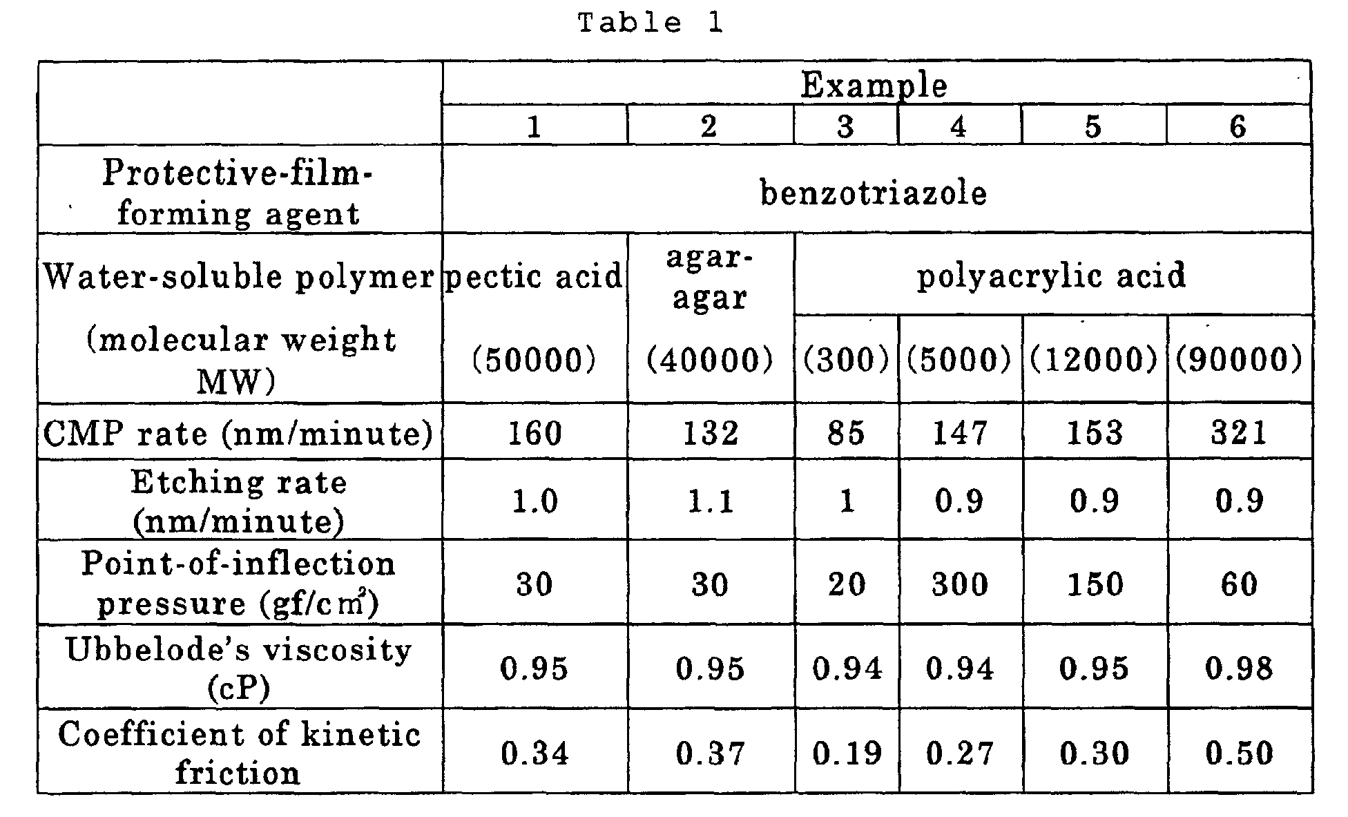
- polishing mediums for CMP were carried out under conditions shown below.
- Substrate member to be polished Silicon substrate with a copper film formed thereon in a thickness of 1 ⁇ m.
- Polishing pad IC1000 (available from Rodel Inc.).
- Polishing pressure 210 gf/cm 2 (point-of-inflection pressure: 0 to 500 gf/cm 2 ).
- Relative speed of substrate member to polishing platen 36 m/minute.
- CMP rate Determined by calculation from electrical resistance value in respect of the difference in layer thickness before and after the copper film was polished by CMP.
- Example 7 8 9 10 11 12
- Protective-film-forming agent benzotriazole Water-soluble polymer (molecular weight polyacrylamide polyvinyl alcohol (1500) (10000) (800000) (23000) (66000) (88000) CMP rate (nm/minute) 162 124 162 132 135 135 Etching rate (nm/minute) 1.0 1.0 1.0 0.9 0.9 0.9 Point-of-inflection pressure (gf/cm 2 ) 60 50 50 90 70 60 Ubbelode's viscosity (cP) 0.94 0.96 0.99 0.97 0.98 0.98 Coefficient of kinetic friction 0.27 0.32 0.35 0.48 0.54 0.57
- a silicon substrate member in which grooves of 0.5 ⁇ m in depth were formed in the insulating layer and a copper film was formed by known sputtering and was buried in the grooves by known heat treatment was subjected to CMP.
- CMP whether or not any erosion and polishing mars occurred was examined by visual observation, optical-microscope observation and electron-microscope observation of the substrate member. As the result, the erosion and the polishing mars were not seen to have occurred in all Examples.
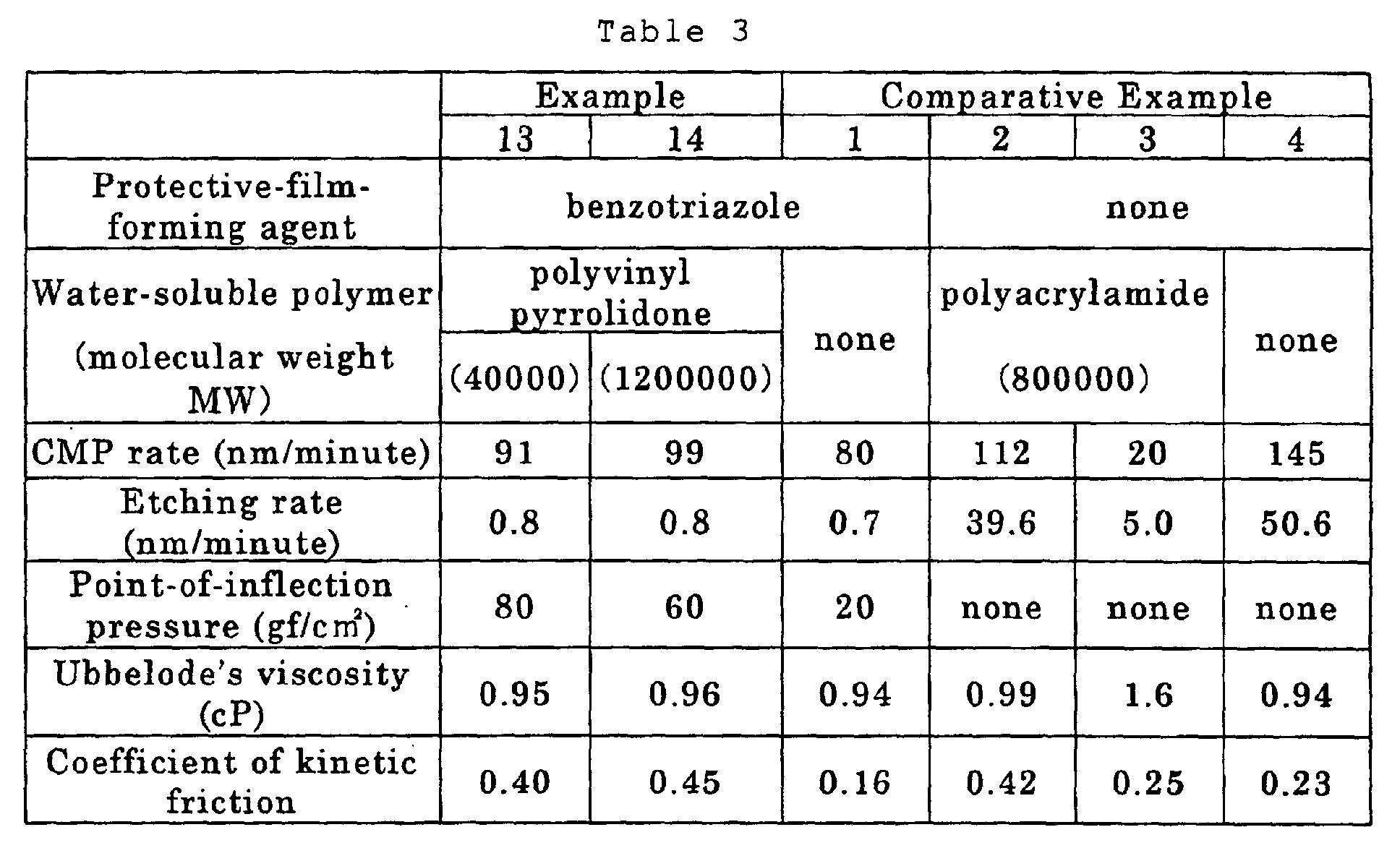
- Comparative Example 1 in which only the protective-film-forming agent was mixed in the polishing medium and the water-soluble polymer was not added, the CMP rate was low. Also, in Comparative Examples 2 and 3, in which only the water-soluble polymer was mixed and the protective-film-forming agent was not added, and in Comparative Example 4, in which both the protective-film-forming agent and the water-soluble polymer were not mixed, the etching rate was so high that the dishing occurred in a large level.
- Examples 1 to 14 in which the protective-film-forming agent and the water-soluble polymer were used in combination, the CMP rate was high although the etching rate was low, making it possible to shorten the polishing time. Moreover, the dishing was only in a small level, and the high flattening was achievable. Also, Examples 4 to 6, in which the molecular weight of the water-soluble polymer was 500 more, showed a higher CMP rate than Example 3, in which it was not more than 500, thus it was found preferable for the water-soluble polymer to have a molecular weight of 500 or more.
- Comparative Example 1 In Comparative Example 1, in which the polishing medium had a coefficient of kinetic friction of 0.16, which was lower than 0.25, the CMP rate was low. Also, the polishing medium of Comparative Example 4, too, having a low coefficient of kinetic friction of 0.23, showed a higher etching rate than the CMP rate, and hence caused the dishing in a large level. In Comparative Examples 1 and 4, having a Ubbelode's viscosity of 0.94 cP, which was lower than 0.95, the CMP rate was low. Also, in Comparative Example 1, having a point-of-inflection pressure of 20 gf/cm 2 , which was lower than 50 gf/cm 2 , the CMP rate was low. Still also, in Comparative Examples 2 to 4, in which the point-of-inflection pressure was not present, the etching rate was so high that the dishing occurred in a large level.
Landscapes
- Chemical & Material Sciences (AREA)
- Organic Chemistry (AREA)
- Engineering & Computer Science (AREA)
- Mechanical Engineering (AREA)
- Dispersion Chemistry (AREA)
- Materials Engineering (AREA)
- Mechanical Treatment Of Semiconductor (AREA)
Abstract
Description
Relative speed of substrate member to polishing platen: 36 m/minute.
| Example | ||||||
| 7 | 8 | 9 | 10 | 11 | 12 | |
| Protective-film-forming agent | benzotriazole | |||||
| Water-soluble polymer (molecular weight | polyacrylamide | polyvinyl alcohol | ||||
| (1500) | (10000) | (800000) | (23000) | (66000) | (88000) | |
| CMP rate (nm/minute) | 162 | 124 | 162 | 132 | 135 | 135 |
| Etching rate (nm/minute) | 1.0 | 1.0 | 1.0 | 0.9 | 0.9 | 0.9 |
| Point-of-inflection pressure (gf/cm2) | 60 | 50 | 50 | 90 | 70 | 60 |
| Ubbelode's viscosity (cP) | 0.94 | 0.96 | 0.99 | 0.97 | 0.98 | 0.98 |
| Coefficient of kinetic friction | 0.27 | 0.32 | 0.35 | 0.48 | 0.54 | 0.57 |
Claims (12)
- A polishing medium for chemical-mechanical polishing, comprising an oxidizing agent, a metal-oxide-dissolving agent, a protective-film-forming agent, a water-soluble polymer, and water.
- The polishing medium for chemical-mechanical polishing according to claim 1, wherein said water-soluble polymer has a weight-average molecular weight of 500 or more.
- The polishing medium for chemical-mechanical polishing according to claim 2, wherein said water-soluble polymer comprises two or more polymers each having a weight-average molecular weight of 500 or more, wherein but a weight-average molecular weight of said polymers are different from each other.
- The polishing medium for chemical-mechanical polishing according to any one of claims 1 to 3, which has a coefficient of kinetic friction of 0.25 or more.
- The polishing medium for chemical-mechanical polishing according to any one of claims 1 to 4, which has a Ubbelode's viscosity of 0.95 cP or more and 1.5 cP or less.
- The polishing medium for chemical-mechanical polishing according to any one of claims 1 to 5, which has a point-of-inflection pressure of 50 gf/cm2.
- The polishing medium for chemical-mechanical polishing according to any one of claims 1 to 6, wherein said oxidizing agent is at least one of hydrogen peroxide, nitric acid, potassium periodate, hypochlorous acid and ozone water.
- The polishing medium for chemical-mechanical polishing according to any one of claims 1 to 7, wherein said metal-oxide-dissolving agent is at least one of an organic acid, an organic-acid ester, an organic-acid ammonium salt and sulfuric acid.
- The polishing medium for chemical-mechanical polishing according to any one of claims 1 to 8, wherein said protective-film-forming agent is a nitrogen-containing compound.
- The polishing medium for chemical-mechanical polishing according to any one of claims 1 to 8, wherein said protective-film-forming agent is at least one of a mercaptan, glucose and cellulose.
- A polishing method comprising polishing a polishing object film of a metal or metal oxide with the polishing medium for chemical-mechanical polishing according to any one of claims 1 to 10.
- The polishing method according to claim 11, wherein said polishing object film comprises at least one of copper, a copper alloy, a copper oxide and a copper alloy oxide.
Applications Claiming Priority (11)
| Application Number | Priority Date | Filing Date | Title |
|---|---|---|---|
| JP23978199 | 1999-08-26 | ||
| JP23977799 | 1999-08-26 | ||
| JP23977999 | 1999-08-26 | ||
| JP23978199 | 1999-08-26 | ||
| JP23977999 | 1999-08-26 | ||
| JP23977899 | 1999-08-26 | ||
| JP23977799 | 1999-08-26 | ||
| JP23977899 | 1999-08-26 | ||
| JP23978099 | 1999-08-26 | ||
| JP23978099 | 1999-08-26 | ||
| PCT/JP2000/005765 WO2001017006A1 (en) | 1999-08-26 | 2000-08-25 | Polishing compound for chemimechanical polishing and polishing method |
Publications (2)
| Publication Number | Publication Date |
|---|---|
| EP1223609A1 true EP1223609A1 (en) | 2002-07-17 |
| EP1223609A4 EP1223609A4 (en) | 2006-03-15 |
Family
ID=27530024
Family Applications (1)
| Application Number | Title | Priority Date | Filing Date |
|---|---|---|---|
| EP00955039A Withdrawn EP1223609A4 (en) | 1999-08-26 | 2000-08-25 | CHEMOMECHANICAL POLISHING COMPOUND AND POLISHING METHOD |
Country Status (7)
| Country | Link |
|---|---|
| US (3) | US7232529B1 (en) |
| EP (1) | EP1223609A4 (en) |
| KR (1) | KR100512453B1 (en) |
| CN (1) | CN1161826C (en) |
| AU (1) | AU6731600A (en) |
| TW (2) | TWI265567B (en) |
| WO (1) | WO2001017006A1 (en) |
Cited By (15)
| Publication number | Priority date | Publication date | Assignee | Title |
|---|---|---|---|---|
| US6605537B2 (en) | 2000-10-27 | 2003-08-12 | Rodel Holdings, Inc. | Polishing of metal substrates |
| WO2004044076A1 (en) * | 2002-11-13 | 2004-05-27 | Dupont Air Products Nanomaterials Llc | A slurry composition and a polishing method using the same |
| US6827752B2 (en) | 2001-05-25 | 2004-12-07 | Ekc Technology K.K. | Cerium oxide slurry, and method of manufacturing substrate |
| EP1505134A1 (en) * | 2003-08-05 | 2005-02-09 | Rohm and Haas Electronic Materials CMP Holdings, Inc. | Chemical mechanical planarization compositions for reducing erosion in semiconductor wafers |
| US7086935B2 (en) | 2004-11-24 | 2006-08-08 | Rohm And Haas Electronic Materials Cmp Holdings, Inc. | Cellulose-containing polishing compositions and methods relating thereto |
| US7300480B2 (en) | 2003-09-25 | 2007-11-27 | Rohm And Haas Electronic Materials Cmp Holdings, Inc. | High-rate barrier polishing composition |
| US7300602B2 (en) | 2003-01-23 | 2007-11-27 | Rohm And Haas Electronic Materials Cmp Holdings, Inc. | Selective barrier metal polishing solution |
| US7303993B2 (en) | 2004-07-01 | 2007-12-04 | Rohm And Haas Electronic Materials Cmp Holdings, Inc. | Chemical mechanical polishing compositions and methods relating thereto |
| GB2443286A (en) * | 2006-08-24 | 2008-04-30 | Fujimi Inc | Polishing composition for semiconductor wafer comprising polyvinylpyrrolidone or poly(N-vinylformamide) |
| US7384871B2 (en) | 2004-07-01 | 2008-06-10 | Rohm And Haas Electronic Materials Cmp Holdings, Inc. | Chemical mechanical polishing compositions and methods relating thereto |
| US7435356B2 (en) | 2004-11-24 | 2008-10-14 | Rohm And Haas Electronic Materials Cmp Holdings, Inc. | Abrasive-free chemical mechanical polishing compositions and methods relating thereto |
| US7497967B2 (en) | 2004-03-24 | 2009-03-03 | Rohm And Haas Electronic Materials Cmp Holdings, Inc. | Compositions and methods for polishing copper |
| EP1909312A4 (en) * | 2005-06-28 | 2010-06-16 | Asahi Glass Co Ltd | ABRASIVE AND PROCESS FOR PRODUCING SEMICONDUCTOR INTEGRATED CIRCUIT UNIT |
| US8080476B2 (en) | 2006-08-02 | 2011-12-20 | Fujimi Incorporated | Polishing composition and polishing process |
| US8864860B2 (en) | 2007-12-28 | 2014-10-21 | Fujimi Incorporated | Polishing composition |
Families Citing this family (25)
| Publication number | Priority date | Publication date | Assignee | Title |
|---|---|---|---|---|
| WO2000039844A1 (en) * | 1998-12-28 | 2000-07-06 | Hitachi Chemical Company, Ltd. | Materials for polishing liquid for metal, polishing liquid for metal, method for preparation thereof and polishing method using the same |
| US7004819B2 (en) | 2002-01-18 | 2006-02-28 | Cabot Microelectronics Corporation | CMP systems and methods utilizing amine-containing polymers |
| WO2004068570A1 (en) * | 2003-01-31 | 2004-08-12 | Hitachi Chemical Co., Ltd. | Cmp polishing compound and polishing method |
| KR100960687B1 (en) * | 2003-06-24 | 2010-06-01 | 엘지디스플레이 주식회사 | Etch solution for collective etching of a double metal layer containing copper (or copper alloy layer) |
| JP2005294798A (en) * | 2004-03-08 | 2005-10-20 | Asahi Glass Co Ltd | Abrasive and polishing method |
| CN100468647C (en) * | 2004-03-08 | 2009-03-11 | 旭硝子株式会社 | Abrasives and grinding methods |
| JP4644434B2 (en) | 2004-03-24 | 2011-03-02 | 株式会社フジミインコーポレーテッド | Polishing composition |
| JP2006086462A (en) * | 2004-09-17 | 2006-03-30 | Fujimi Inc | Polishing composition and method for producing wiring structure using the same |
| KR100645957B1 (en) * | 2004-10-26 | 2006-11-14 | 삼성코닝 주식회사 | Aqueous slurry composition for chemical mechanical planarization |
| KR101254523B1 (en) * | 2004-11-02 | 2013-04-19 | 스미토모 베이클라이트 가부시키가이샤 | Epoxy resin composition and semiconductor device |
| JPWO2006112377A1 (en) | 2005-04-14 | 2008-12-11 | 三井化学株式会社 | Abrasive slurry and abrasive using the same |
| KR100624231B1 (en) * | 2005-05-24 | 2006-09-13 | 이상첨 | Eco-friendly sandwich lightweight panel manufacturing method |
| US7435162B2 (en) * | 2005-10-24 | 2008-10-14 | 3M Innovative Properties Company | Polishing fluids and methods for CMP |
| KR101260597B1 (en) * | 2005-12-27 | 2013-05-06 | 히타치가세이가부시끼가이샤 | Metal polishing liquid and method for polishing film to be polished |
| US8147712B2 (en) | 2006-03-20 | 2012-04-03 | Mitsui Chemicals, Inc. | Polishing composition |
| CN101410956B (en) * | 2006-04-03 | 2010-09-08 | Jsr株式会社 | Aqueous dispersion for chemical mechanical polishing and chemical mechanical polishing method |
| WO2008044477A1 (en) * | 2006-10-06 | 2008-04-17 | Jsr Corporation | Aqueous dispersion for chemical mechanical polishing and chemical mechanical polishing method for semiconductor device |
| TWI367524B (en) * | 2007-08-01 | 2012-07-01 | Univ Nat Taiwan Science Tech | Chemical mechanical polishing apparatus and chemical mechanical polishing method thereof |
| US8506661B2 (en) * | 2008-10-24 | 2013-08-13 | Air Products & Chemicals, Inc. | Polishing slurry for copper films |
| US20110177623A1 (en) * | 2010-01-15 | 2011-07-21 | Confluense Llc | Active Tribology Management of CMP Polishing Material |
| JP5587620B2 (en) * | 2010-01-25 | 2014-09-10 | 株式会社フジミインコーポレーテッド | Polishing composition and polishing method using the same |
| US8821215B2 (en) | 2012-09-07 | 2014-09-02 | Cabot Microelectronics Corporation | Polypyrrolidone polishing composition and method |
| US9815683B1 (en) | 2016-10-11 | 2017-11-14 | Fuel Automation Station, LLC | Method and system for mobile distribution station |
| US20210079263A1 (en) * | 2019-09-17 | 2021-03-18 | Fujimi Incorporated | High molecular weight polyvinyl pyrrolidone for low-k removal rate suppresion |
| CN116814167B (en) * | 2023-06-15 | 2025-07-11 | 大连理工大学 | Chemical mechanical polishing solution suitable for fused quartz and containing dissolved silk and preparation method and application thereof |
Family Cites Families (43)
| Publication number | Priority date | Publication date | Assignee | Title |
|---|---|---|---|---|
| US3855146A (en) * | 1971-03-03 | 1974-12-17 | Fuji Photo Film Co Ltd | Process for preparing microscopic capsules containing hydrophobic oil droplets therein |
| US4752628A (en) | 1987-05-15 | 1988-06-21 | Nalco Chemical Company | Concentrated lapping slurries |
| DE68927116T2 (en) * | 1988-01-19 | 1997-02-06 | Fujimi Inc | Polishing compound |
| US5484605A (en) * | 1988-11-25 | 1996-01-16 | Henning Berlin Gmbh Chemie-Und Pharmawerk | Agent for treating chronically inflammatory intestinal diseases |
| US5352277A (en) | 1988-12-12 | 1994-10-04 | E. I. Du Pont De Nemours & Company | Final polishing composition |
| JPH05104436A (en) | 1991-10-17 | 1993-04-27 | Fanuc Ltd | Tactile sensor integrated type polishing processing machine |
| TW263531B (en) | 1992-03-11 | 1995-11-21 | Mitsubishi Gas Chemical Co | |
| US5607718A (en) * | 1993-03-26 | 1997-03-04 | Kabushiki Kaisha Toshiba | Polishing method and polishing apparatus |
| US5630950A (en) * | 1993-07-09 | 1997-05-20 | Enthone-Omi, Inc. | Copper brightening process and bath |
| JP3556978B2 (en) * | 1993-12-14 | 2004-08-25 | 株式会社東芝 | Polishing method for copper-based metal |
| JP3397501B2 (en) | 1994-07-12 | 2003-04-14 | 株式会社東芝 | Abrasive and polishing method |
| US5860848A (en) | 1995-06-01 | 1999-01-19 | Rodel, Inc. | Polishing silicon wafers with improved polishing slurries |
| JP3192968B2 (en) | 1995-06-08 | 2001-07-30 | 株式会社東芝 | Polishing liquid for copper-based metal and method for manufacturing semiconductor device |
| JPH0963996A (en) | 1995-08-29 | 1997-03-07 | Nippon Steel Corp | Silicon wafer polishing method |
| JP3514908B2 (en) | 1995-11-13 | 2004-04-05 | 株式会社東芝 | Abrasive |
| US5743784A (en) * | 1995-12-19 | 1998-04-28 | Applied Materials, Inc. | Apparatus and method to determine the coefficient of friction of a chemical mechanical polishing pad during a pad conditioning process and to use it to control the process |
| KR970042941A (en) * | 1995-12-29 | 1997-07-26 | 베일리 웨인 피 | Polishing Compounds for Mechanical and Chemical Polishing Processes |
| JPH09194824A (en) | 1996-01-12 | 1997-07-29 | Sanyo Chem Ind Ltd | Water-soluble lapping fluid composition |
| EP0786504A3 (en) * | 1996-01-29 | 1998-05-20 | Fujimi Incorporated | Polishing composition |
| US5779910A (en) * | 1996-04-08 | 1998-07-14 | Cytec Technology Corp. | Enhanced flocculation of mineral slurry with polymer blends |
| US5780358A (en) * | 1996-04-08 | 1998-07-14 | Chartered Semiconductor Manufacturing Ltd. | Method for chemical-mechanical polish (CMP) planarizing of cooper containing conductor layers |
| JP3462052B2 (en) | 1996-09-30 | 2003-11-05 | 日立化成工業株式会社 | Cerium oxide abrasive and substrate polishing method |
| US6007592A (en) * | 1996-11-14 | 1999-12-28 | Nissan Chemical Industries, Ltd. | Polishing composition for aluminum disk and polishing process therewith |
| US5954997A (en) * | 1996-12-09 | 1999-09-21 | Cabot Corporation | Chemical mechanical polishing slurry useful for copper substrates |
| US5876490A (en) * | 1996-12-09 | 1999-03-02 | International Business Machines Corporatin | Polish process and slurry for planarization |
| US6309560B1 (en) | 1996-12-09 | 2001-10-30 | Cabot Microelectronics Corporation | Chemical mechanical polishing slurry useful for copper substrates |
| US5876268A (en) * | 1997-01-03 | 1999-03-02 | Minnesota Mining And Manufacturing Company | Method and article for the production of optical quality surfaces on glass |
| WO1998049723A1 (en) * | 1997-04-30 | 1998-11-05 | Minnesota Mining And Manufacturing Company | Method of planarizing the upper surface of a semiconductor wafer |
| US6194317B1 (en) * | 1998-04-30 | 2001-02-27 | 3M Innovative Properties Company | Method of planarizing the upper surface of a semiconductor wafer |
| JPH10321566A (en) | 1997-05-19 | 1998-12-04 | Asahi Chem Ind Co Ltd | Method for polishing semiconductor device |
| TW429271B (en) | 1997-10-10 | 2001-04-11 | Applied Materials Inc | Introducing process fluid over rotating substrates |
| JP4115562B2 (en) | 1997-10-14 | 2008-07-09 | 株式会社フジミインコーポレーテッド | Polishing composition |
| JP3371775B2 (en) | 1997-10-31 | 2003-01-27 | 株式会社日立製作所 | Polishing method |
| JP3970439B2 (en) | 1997-10-31 | 2007-09-05 | 株式会社ルネサステクノロジ | Manufacturing method of semiconductor device |
| TW455626B (en) | 1998-07-23 | 2001-09-21 | Eternal Chemical Co Ltd | Chemical mechanical abrasive composition for use in semiconductor processing |
| AU5445899A (en) | 1998-08-31 | 2000-03-21 | Hitachi Chemical Company, Ltd. | Abrasive liquid for metal and method for polishing |
| WO2000039844A1 (en) * | 1998-12-28 | 2000-07-06 | Hitachi Chemical Company, Ltd. | Materials for polishing liquid for metal, polishing liquid for metal, method for preparation thereof and polishing method using the same |
| US6402978B1 (en) | 1999-05-06 | 2002-06-11 | Mpm Ltd. | Magnetic polishing fluids for polishing metal substrates |
| US20010054706A1 (en) * | 1999-07-19 | 2001-12-27 | Joseph A. Levert | Compositions and processes for spin etch planarization |
| TW501197B (en) | 1999-08-17 | 2002-09-01 | Hitachi Chemical Co Ltd | Polishing compound for chemical mechanical polishing and method for polishing substrate |
| KR20020027571A (en) | 1999-08-24 | 2002-04-13 | 갤반 마틴 | Compositions for insulator and metal cmp and methods relating thereto |
| US6319096B1 (en) * | 1999-11-15 | 2001-11-20 | Cabot Corporation | Composition and method for planarizing surfaces |
| JP2002050595A (en) * | 2000-08-04 | 2002-02-15 | Hitachi Ltd | Polishing method, wiring forming method, and semiconductor device manufacturing method |
-
2000
- 2000-08-25 TW TW089117424A patent/TWI265567B/en not_active IP Right Cessation
- 2000-08-25 CN CNB008119635A patent/CN1161826C/en not_active Expired - Lifetime
- 2000-08-25 US US10/069,404 patent/US7232529B1/en not_active Expired - Lifetime
- 2000-08-25 AU AU67316/00A patent/AU6731600A/en not_active Abandoned
- 2000-08-25 KR KR10-2002-7002466A patent/KR100512453B1/en not_active Expired - Lifetime
- 2000-08-25 WO PCT/JP2000/005765 patent/WO2001017006A1/en not_active Ceased
- 2000-08-25 TW TW093135637A patent/TWI290740B/en not_active IP Right Cessation
- 2000-08-25 EP EP00955039A patent/EP1223609A4/en not_active Withdrawn
-
2006
- 2006-04-21 US US11/407,903 patent/US20060186373A1/en not_active Abandoned
-
2007
- 2007-04-19 US US11/737,502 patent/US20070190906A1/en not_active Abandoned
Cited By (20)
| Publication number | Priority date | Publication date | Assignee | Title |
|---|---|---|---|---|
| US6605537B2 (en) | 2000-10-27 | 2003-08-12 | Rodel Holdings, Inc. | Polishing of metal substrates |
| US6827752B2 (en) | 2001-05-25 | 2004-12-07 | Ekc Technology K.K. | Cerium oxide slurry, and method of manufacturing substrate |
| WO2004044076A1 (en) * | 2002-11-13 | 2004-05-27 | Dupont Air Products Nanomaterials Llc | A slurry composition and a polishing method using the same |
| US7300602B2 (en) | 2003-01-23 | 2007-11-27 | Rohm And Haas Electronic Materials Cmp Holdings, Inc. | Selective barrier metal polishing solution |
| EP1505134A1 (en) * | 2003-08-05 | 2005-02-09 | Rohm and Haas Electronic Materials CMP Holdings, Inc. | Chemical mechanical planarization compositions for reducing erosion in semiconductor wafers |
| US7300603B2 (en) | 2003-08-05 | 2007-11-27 | Rohm And Haas Electronic Materials Cmp Holdings, Inc. | Chemical mechanical planarization compositions for reducing erosion in semiconductor wafers |
| US7300480B2 (en) | 2003-09-25 | 2007-11-27 | Rohm And Haas Electronic Materials Cmp Holdings, Inc. | High-rate barrier polishing composition |
| US7497967B2 (en) | 2004-03-24 | 2009-03-03 | Rohm And Haas Electronic Materials Cmp Holdings, Inc. | Compositions and methods for polishing copper |
| US7384871B2 (en) | 2004-07-01 | 2008-06-10 | Rohm And Haas Electronic Materials Cmp Holdings, Inc. | Chemical mechanical polishing compositions and methods relating thereto |
| US7303993B2 (en) | 2004-07-01 | 2007-12-04 | Rohm And Haas Electronic Materials Cmp Holdings, Inc. | Chemical mechanical polishing compositions and methods relating thereto |
| US7435356B2 (en) | 2004-11-24 | 2008-10-14 | Rohm And Haas Electronic Materials Cmp Holdings, Inc. | Abrasive-free chemical mechanical polishing compositions and methods relating thereto |
| US7086935B2 (en) | 2004-11-24 | 2006-08-08 | Rohm And Haas Electronic Materials Cmp Holdings, Inc. | Cellulose-containing polishing compositions and methods relating thereto |
| KR101101169B1 (en) * | 2004-11-24 | 2012-01-05 | 롬 앤드 하스 일렉트로닉 머티리얼스 씨엠피 홀딩스 인코포레이티드 | Abrasive-free chemical mechanical polishing compositions and methods associated therewith |
| EP1909312A4 (en) * | 2005-06-28 | 2010-06-16 | Asahi Glass Co Ltd | ABRASIVE AND PROCESS FOR PRODUCING SEMICONDUCTOR INTEGRATED CIRCUIT UNIT |
| US8080476B2 (en) | 2006-08-02 | 2011-12-20 | Fujimi Incorporated | Polishing composition and polishing process |
| GB2443286A (en) * | 2006-08-24 | 2008-04-30 | Fujimi Inc | Polishing composition for semiconductor wafer comprising polyvinylpyrrolidone or poly(N-vinylformamide) |
| US7867909B2 (en) | 2006-08-24 | 2011-01-11 | Fujimi Incorporated | Polishing composition and polishing method |
| GB2443286B (en) * | 2006-08-24 | 2011-11-23 | Fujimi Inc | Polishing composition and polishing method |
| US8721909B2 (en) | 2006-08-24 | 2014-05-13 | Fujimi Incorporated | Polishing composition and polishing method |
| US8864860B2 (en) | 2007-12-28 | 2014-10-21 | Fujimi Incorporated | Polishing composition |
Also Published As
| Publication number | Publication date |
|---|---|
| AU6731600A (en) | 2001-03-26 |
| KR20020042814A (en) | 2002-06-07 |
| US7232529B1 (en) | 2007-06-19 |
| CN1371529A (en) | 2002-09-25 |
| TWI290740B (en) | 2007-12-01 |
| EP1223609A4 (en) | 2006-03-15 |
| TWI265567B (en) | 2006-11-01 |
| US20070190906A1 (en) | 2007-08-16 |
| KR100512453B1 (en) | 2005-09-07 |
| WO2001017006A1 (en) | 2001-03-08 |
| CN1161826C (en) | 2004-08-11 |
| TW200511421A (en) | 2005-03-16 |
| US20060186373A1 (en) | 2006-08-24 |
Similar Documents
| Publication | Publication Date | Title |
|---|---|---|
| US7232529B1 (en) | Polishing compound for chemimechanical polishing and polishing method | |
| EP2242091B1 (en) | Polishing solution for metal and polishing method | |
| US20030219982A1 (en) | CMP (chemical mechanical polishing) polishing liquid for metal and polishing method | |
| JP2001127018A (en) | Metal polishing method | |
| JP2001144060A (en) | Method of polishing substrate having metallic laminated film | |
| JP3902897B2 (en) | Substrate polishing method using metal polishing liquid | |
| JP2001144044A (en) | Metal polishing fluid and polishing method using it | |
| JP2002208573A (en) | Polishing liquid for metal and polishing method | |
| JP2001144055A (en) | Method of polishing substrate having metallic laminated film | |
| JP2001127027A (en) | Metal polishing method | |
| JP4062903B2 (en) | Polishing liquid for metal and polishing method | |
| JP2007019531A (en) | Abrasive for chemical mechanical polishing, and polishing method | |
| JP3627598B2 (en) | Polishing liquid for metal and polishing method | |
| JP3902896B2 (en) | Polishing liquid for metal and substrate polishing method using the same | |
| JP4486774B2 (en) | Polishing liquid for metal and polishing method using the same | |
| JP2001127017A (en) | Metal polishing method | |
| JP2001144047A (en) | Metal polishing fluid and polishing method using it | |
| JP2002198332A (en) | Metal polishing liquid and polishing method using it | |
| JP2001144052A (en) | Method of polishing substrate | |
| JP2002176015A (en) | Polishing liquid for metal and polishing method | |
| JP2002198333A (en) | Metal polishing liquid and substrate polishing method using it | |
| JP2001144042A (en) | Metal polishing method | |
| JP2001144043A (en) | Polishing method for board with layered metal film | |
| JP2001127023A (en) | Metal polishing method | |
| JP2007180568A (en) | Polishing compound for chemimechanical polishing and polishing method |
Legal Events
| Date | Code | Title | Description |
|---|---|---|---|
| PUAI | Public reference made under article 153(3) epc to a published international application that has entered the european phase |
Free format text: ORIGINAL CODE: 0009012 |
|
| 17P | Request for examination filed |
Effective date: 20020302 |
|
| AK | Designated contracting states |
Kind code of ref document: A1 Designated state(s): AT BE CH CY DE DK ES FI FR GB GR IE IT LI LU MC NL PT SE |
|
| AX | Request for extension of the european patent |
Free format text: AL;LT;LV;MK;RO;SI |
|
| RBV | Designated contracting states (corrected) |
Designated state(s): AT BE CH CY DE FR GB IT LI NL |
|
| RIC1 | Information provided on ipc code assigned before grant |
Ipc: H01L 21/321 20060101AFI20060119BHEP Ipc: C11D 11/00 20060101ALI20060119BHEP |
|
| A4 | Supplementary search report drawn up and despatched |
Effective date: 20060126 |
|
| 17Q | First examination report despatched |
Effective date: 20061017 |
|
| STAA | Information on the status of an ep patent application or granted ep patent |
Free format text: STATUS: THE APPLICATION HAS BEEN WITHDRAWN |
|
| 18W | Application withdrawn |
Effective date: 20100219 |