EP1222735B1 - Interface acoustic wave filter, especially for wireless connections - Google Patents
Interface acoustic wave filter, especially for wireless connections Download PDFInfo
- Publication number
- EP1222735B1 EP1222735B1 EP00966253A EP00966253A EP1222735B1 EP 1222735 B1 EP1222735 B1 EP 1222735B1 EP 00966253 A EP00966253 A EP 00966253A EP 00966253 A EP00966253 A EP 00966253A EP 1222735 B1 EP1222735 B1 EP 1222735B1
- Authority
- EP
- European Patent Office
- Prior art keywords
- interface
- bodies
- piezoelectric
- plane
- acoustic
- Prior art date
- Legal status (The legal status is an assumption and is not a legal conclusion. Google has not performed a legal analysis and makes no representation as to the accuracy of the status listed.)
- Revoked
Links
Images


Classifications
-
- H—ELECTRICITY
- H03—ELECTRONIC CIRCUITRY
- H03H—IMPEDANCE NETWORKS, e.g. RESONANT CIRCUITS; RESONATORS
- H03H9/00—Networks comprising electromechanical or electro-acoustic devices; Electromechanical resonators
- H03H9/02—Details
- H03H9/0222—Details of interface-acoustic, boundary, pseudo-acoustic or Stonely wave devices
-
- H—ELECTRICITY
- H03—ELECTRONIC CIRCUITRY
- H03H—IMPEDANCE NETWORKS, e.g. RESONANT CIRCUITS; RESONATORS
- H03H9/00—Networks comprising electromechanical or electro-acoustic devices; Electromechanical resonators
- H03H9/46—Filters
- H03H9/64—Filters using surface acoustic waves
Definitions
- the present invention as defined in the claims relates to an acoustic wave filter of planar structure, that is, in which acoustic waves propagate in a plane.
- wireless communication links such as those used in mobile telephony or keys intended for remote control of the opening of the doors of an automobile, or even in exchange without data wire between relocated electrical or computer devices.
- These wireless links use overhead filters, called RF (Radio Frequency Filters) and IF intermediate frequency filters with surface acoustic waves (Surface Acoustic Wave Filters).
- a surface acoustic wave filter is generally constituted by a piezoelectric substrate which under the effect of an electric field generates acoustic waves which propagate on the surface of the substrate, these waves being either located in the sagittal plane (Rayleigh waves ), either oriented transversely (Bleustein-Gulayev waves) or almost transversely with respect to their direction of propagation.
- the substrate comprises a planar metallic structure formed by a metallic deposit deposited on the substrate or buried in grooves formed on its surface, this planar metallic structure comprising a plurality of fingers forming for example interdigitated combs, or forming a SPUDT transducer (Single Phase UniDirectional Transducer), R-SPUDT type (Resonant SPUDT) or acoustically coupled resonators or electrically.
- SPUDT transducer Single Phase UniDirectional Transducer
- R-SPUDT type Resonant SPUDT
- acoustically coupled resonators or electrically electrically.
- the carrier frequencies used in mobile telephony have tendency to increase, from 900 MHz to 1800 MHz, to reach 2200 MHz, even 3000 MHz and more.
- the size of the substrate, the interval between the fingers and especially the dimension of the fingers of the metallic structure must therefore be reduced accordingly to be able to process such high frequencies. So, the precision of the lithography machines necessary for producing the engravings metal must go from 0.5 ⁇ m to 0.35 ⁇ m, or even much less (0.25 to 0.18 .mu.m).
- the presence of the slightest dust or projection of material degrades the performance of the filter, all the more so since the dimensions of the substrate must be increasingly reduced. It is therefore necessary that the substrate is protected by a housing.
- the substrate is piezoelectric, it must also be protected from electromagnetic disturbances. Therefore, the housing must be shielded.
- the present invention aims to eliminate these drawbacks. To this end, it offers a flat structure acoustic filter in which acoustic waves propagate substantially in a plane.
- this filter is characterized in that it comprises two solid bodies at least one of which is piezoelectric, these bodies being linked to each other by so as to present a plane interface between them, the acoustic waves being generated by the piezoelectric body by means of an electric field, the waves acoustic being guided by the interface between the two solid bodies and having acoustic energy which exponentially decreases in both bodies from of the interface in a direction perpendicular to the interface.
- the acoustic waves propagate not on the surface of a substrate, but at the interface between two solid bodies.
- the energy of these waves exponentially decreases in the two solid bodies from the interface, if although no energy comes out of the structure when the thickness of the solid bodies is greater than a few tens of times the wavelength of acoustic waves. Therefore, no case is necessary to protect the component (filter) from its environment.
- the acoustic waves propagating at the interface between two media solid they can have a higher propagation speed than surface waves (for example 5000 m / s instead of 3000 m / s).
- interface waves which are non-dispersive, can exhibit two types of main polarization: when the vector displaces the atoms of matter is located only in the sagittal plane (perpendicular to the interface plane), this are the Stoneley waves, when this displacement vector is located only in the direction perpendicular to the sagittal plane these are the interface waves of Maerfeld-Tournois.
- a more detailed description of these waves is for example given in documents [1], [2] and [3] mentioned at the end of this description and which are incorporated into this description by way of reference.
- transverse or quasi interface waves are used.
- transverse whose conditions of existence are less drastic than those Stoneley waves and whose propagation speed is generally more big.
- the crystallographic axes of the materials constituting the two bodies are chosen so that the transverse component of the vector displacement of the wave in the plane of the interface is the only component of the displacement vector or is dominant, and the wave is coupled piezoelectrically.
- the two bodies can be made of a piezoelectric material or the of them.
- the two piezoelectric materials can be identical. They can also be assembled so as to present the same crystalline orientations to form a single solid body.
- flat metallic structure forming the filter, formed at the interface between the two body serves as a piezoelectric guide for the transverse interface wave (SH) or quasi-transverse (Q-SH).
- the crystallographic axes of the piezoelectric material are preferably chosen in such a way that according to the direction of propagation, the vector of displacement of the acoustic waves is purely transverse-horizontal or has a dominant transverse-horizontal component, and such that these waves are piezoelectrically coupled.
- the crystallographic axes of the non-piezoelectric material can also be chosen so that, according to the direction of propagation chosen, the displacement vector of the acoustic waves is purely transverse-horizontal or has a dominant transverse-horizontal component, and such that these waves have a speed of propagation equal to or greater than the propagation speed of the transverse-horizontal or quasi-transverse-horizontal waves in the piezoelectric material.
- the dielectric constant and the density of the non piezoelectric material are less than the constant respectively dielectric and density of the piezoelectric material.
- FIG. 1 shows an acoustic wave filter according to this invention.
- This filter comprises two solid bodies 1, 2 for example of shape parallelepiped, having one face against the other so as to form a interface 3 located in an xOz plane.
- One 1 of the two solid bodies 1, 2 is in one material A piezoelectric, while the other is of material B piezoelectric, identical or not to material A, or else not piezoelectric.
- the crystallographic axes of bodies 1 and 2 are chosen so that if acoustic waves 5 propagating in the direction Ox are generated, near the interface plane 3, the energy of these waves decreases exponentially in both bodies from the interface in a direction Oy perpendicular to this one, as the exponential curves show 6. In this way, no energy comes out of the structure, if bodies 1 and 2 are sufficiently thick (in the direction Oy in FIG. 1), of the order of a few tens of times the wavelength of acoustic waves.
- These waves which are non-dispersive, can have two main types of polarization: when the displacement vector 7 of the atoms of matter is located only in the sagittal plane xOy, these are the Stoneley waves (see reference [1]), when this displacement vector is located only in the direction Oz perpendicular to the sagittal plane (case of the wave shown in Figure 1), these are transverse Maerfeld-Tournois interface waves (see references [2] and [3]) .
- the filter according to the invention uses interface waves whose conditions of existence are less drastic than those of Stoneley waves and whose propagation speed is generally greater.
- the acoustic wave filter comprises, placed at interface 3 between the two materials A and B, a flat filter structure conductive, e.g. metallic, similar to that of wave components surface, such as interdigital combs (see reference [4]), SPUDT (see reference [5]) or R-SPUDT (see reference [6]) transducers, and wave resonators acoustically coupled (see reference [7]) or coupled electrically (see reference [8]).
- This conductive structure makes it possible to generate the acoustic waves, the shape and the arrangement of this structure defining the filter characteristics.
- This structure is for example constituted by a network of conductors electric obtained by a metallic deposit formed at the interface between the two body 1, 2, buried in furrows dug in one of the two bodies 1, 2 to the interface 3, for example in the body 1. It comprises for example two reflectors consisting of segments of conductors 9, 9 'perpendicular to the direction of propagation of the acoustic waves, and between the segments of conductors 9 and 9 ', a transducer consisting of two interdigitated combs 10, by having a plurality of fingers.
- the two materials are piezoelectric
- ⁇ A and ⁇ B are the dielectric constants of the materials A and B
- e A and e B are the coefficients (e 15 ) A and (e 15 ) B of the piezoelectric tensors
- v A and v B are the transverse propagation velocities of these acoustic waves in materials A and B.
- K 2 being the piezoelectric coupling coefficient of the material.
- the interface wave is degenerate and merges with the transverse wave of speed volume v S.
- the interface wave exists and is not degenerate, and its speed v is close to the speed v CC .
- SH pure transverse interface wave
- PZT lead and zirconium titanate
- One of the two bodies is piezoelectric and the other nonpiezoelectric
- a purely transverse interface acoustic wave can exist between two materials, one of which is non-piezoelectric with density ⁇ NP and speed v NP and the other piezoelectric with density ⁇ P and speed v P , chosen from the crystal class 6 mm with the crystallographic axis C in the plane xOz of the interface, perpendicular to the direction of propagation Ox of the wave ( Figure 1).
- the coupling coefficient will therefore be all the greater as K 2 will be large, that ⁇ NP will be less than ⁇ P and that ⁇ NP will be less than ⁇ P.
- materials 1 to 8 are piezoelectric and materials 9 to 12 non piezoelectric.
- one of the materials on the surface of one of the materials, one deposit or bury in engraved furrows of controlled thickness along the axes the metal structure of the flat filter, as shown in Figure 2. Then the other material is adhered to this surface along the axes suitable for using any conceivable method of elastic adhesion.
- a non-piezoelectric YAG crystal can be adhered to a piezoelectric Lithium Niobate (LiNbO 3 ) crystal or to a piezoelectric Lithium Tantalate (LiTaO 3 ) crystal, cut along the crystallographic axis Y, the propagation taking place along the crystallographic axis X.
- LiNbO 3 piezoelectric Lithium Niobate
- LiTaO 3 piezoelectric Lithium Tantalate
- one of the two bodies 1, 2 is crystalline and the other is obtained by deposition or epitaxy.
- the metal structure which composes the flat filter and deposits or forms the second material by epitaxy along the axes appropriate to the surface thus prepared of the crystalline material we deposit or bury it in furrows engraved with controlled thickness, along the appropriate axes, the metal structure which composes the flat filter and deposits or forms the second material by epitaxy along the axes appropriate to the surface thus prepared of the crystalline material.
- Non-piezoelectric amorphous silicon Si
- a piezoelectric Lithium Niobate YX-LiNbO 3 a surface thus prepared of piezoelectric Lithium Niobate YX-LiNbO 3 , of section Y (where Y is rotated by a certain angle), the propagation taking place along the axis X.
- a piezoelectric layer of Aluminum Nitride (AlN) can also be formed by epitaxy on a surface of non piezoelectric Sapphire (Al 2 O 3 ).
Abstract
Description
La présente invention telle que definie dans les revendications concerne un filtre à ondes acoustiques de structure plane, c'est-à-dire dans lequel des ondes acoustiques se propagent dans un plan.The present invention as defined in the claims relates to an acoustic wave filter of planar structure, that is, in which acoustic waves propagate in a plane.
Elle s'applique notamment, mais non exclusivement, aux liaisons de
communication sans fil comme celles utilisées dans la téléphonie mobile ou les
clés destinées à la commande à distance de l'ouverture des portes d'une
automobile, ou encore dans l'échange sans fil de données entre appareils
électriques ou informatiques délocalisés.
Ces liaisons sans fil utilisent des filtres en tête, appelés RF (Radio Frequency
Filters) et des filtres de fréquence intermédiaire FI à ondes acoustiques de surface
(Surface Acoustic Wave Filters).It applies in particular, but not exclusively, to wireless communication links such as those used in mobile telephony or keys intended for remote control of the opening of the doors of an automobile, or even in exchange without data wire between relocated electrical or computer devices.
These wireless links use overhead filters, called RF (Radio Frequency Filters) and IF intermediate frequency filters with surface acoustic waves (Surface Acoustic Wave Filters).
Un filtre à ondes acoustiques de surface est généralement constitué par un
substrat piézoélectrique qui sous l'effet d'un champ électrique génère des ondes
acoustiques qui se propagent à la surface du substrat, ces ondes étant soit situées
dans le plan sagittal (ondes de Rayleigh), soit orientées transversalement (ondes
de Bleustein-Gulayev) ou quasi transversalement par rapport à leur direction de
propagation.
Pour générer ces ondes acoustiques, le substrat comprend une structure
métallique plane formée par un dépôt métallique déposé sur le substrat ou enterré
dans des sillons formés à sa surface, cette structure métallique plane comprenant
une pluralité de doigts formant par exemple des peignes interdigités, ou formant
un transducteur de type SPUDT (Single Phase UniDirectional Transducer), de
type R-SPUDT (Resonant SPUDT) ou des résonateurs couplés acoustiquement
ou électriquement. Pour plus d'informations sur ces dispositifs, on peut se référer
aux documents [4] à [8] qui sont mentionnés dans la liste des références figurant
à la fin de la présente description, et qui sont incorporés dans la présente
description à titre de référence.A surface acoustic wave filter is generally constituted by a piezoelectric substrate which under the effect of an electric field generates acoustic waves which propagate on the surface of the substrate, these waves being either located in the sagittal plane (Rayleigh waves ), either oriented transversely (Bleustein-Gulayev waves) or almost transversely with respect to their direction of propagation.
To generate these acoustic waves, the substrate comprises a planar metallic structure formed by a metallic deposit deposited on the substrate or buried in grooves formed on its surface, this planar metallic structure comprising a plurality of fingers forming for example interdigitated combs, or forming a SPUDT transducer (Single Phase UniDirectional Transducer), R-SPUDT type (Resonant SPUDT) or acoustically coupled resonators
or electrically. For more information on these devices, reference can be made to documents [4] to [8] which are mentioned in the list of references appearing at the end of this description, and which are incorporated in this description by way of reference.
Les avantages des filtres à ondes acoustiques de surface par rapport aux filtres utilisant une autre technologie résident dans leurs très faibles dimensions, leur faible consommation (ce sont des filtres passifs) et surtout leur faible coût de fabrication.The advantages of surface acoustic wave filters compared to filters using another technology resides in their very small dimensions, their low consumption (these are passive filters) and above all their low cost of manufacturing.
Toutefois, les fréquences porteuses utilisées dans la téléphonie mobile ont tendance à augmenter, depuis 900 MHz à 1800 MHz, pour atteindre 2200 MHz, voire 3000 MHz et plus. La taille du substrat, l'intervalle entre les doigts et surtout la dimension des doigts de la structure métallique doivent donc être réduites en conséquence pour pouvoir traiter des fréquences aussi élevées. Ainsi, la précision des machines de lithographie nécessaire à la réalisation des gravures métalliques doit passer de 0,5 µm à 0,35 µm, voire beaucoup moins (0,25 à 0,18 µm).However, the carrier frequencies used in mobile telephony have tendency to increase, from 900 MHz to 1800 MHz, to reach 2200 MHz, even 3000 MHz and more. The size of the substrate, the interval between the fingers and especially the dimension of the fingers of the metallic structure must therefore be reduced accordingly to be able to process such high frequencies. So, the precision of the lithography machines necessary for producing the engravings metal must go from 0.5 µm to 0.35 µm, or even much less (0.25 to 0.18 .mu.m).
Par ailleurs la présence de la moindre poussière ou projection de matière dégrade
les performances du filtre, et ce d'autant plus que les dimensions du substrat
doivent être de plus en plus réduites.
Il est donc nécessaire que le substrat soit protégé par un boítier.
En outre, comme le substrat est piézoélectrique, il doit également être protégé
des perturbations électromagnétiques. Par conséquent, le boítier doit être blindé.Furthermore, the presence of the slightest dust or projection of material degrades the performance of the filter, all the more so since the dimensions of the substrate must be increasingly reduced.
It is therefore necessary that the substrate is protected by a housing.
In addition, as the substrate is piezoelectric, it must also be protected from electromagnetic disturbances. Therefore, the housing must be shielded.
Il en résulte donc un problème de structure du coût des composants, puisqu'en devenant de plus en plus petites, les puces acoustiques vont coûter beaucoup moins cher que le boítier destiné à protéger la puce de l'environnement.This therefore results in a structural problem of the cost of the components, since in getting smaller and smaller, the acoustic chips will cost a lot cheaper than the case intended to protect the chip from the environment.
La présente invention a pour but de supprimer ces inconvénients. A cet effet, elle propose un filtre acoustique de structure plane dans lequel des ondes acoustiques se propagent sensiblement dans un plan.The present invention aims to eliminate these drawbacks. To this end, it offers a flat structure acoustic filter in which acoustic waves propagate substantially in a plane.
Selon l'invention, ce filtre est caractérisé en ce qu'il comprend deux corps solides dont l'un au moins est piézoélectrique, ces corps étant liés l'un à l'autre de manière à présenter une interface plane entre eux, les ondes acoustiques étant générées par le corps piézoélectrique au moyen d'un champ électrique, les ondes acoustiques étant guidées par l'interface entre les deux corps solides et présentant une énergie acoustique qui décroít exponentiellement dans les deux corps à partir de l'interface dans une direction perpendiculaire à l'interface. According to the invention, this filter is characterized in that it comprises two solid bodies at least one of which is piezoelectric, these bodies being linked to each other by so as to present a plane interface between them, the acoustic waves being generated by the piezoelectric body by means of an electric field, the waves acoustic being guided by the interface between the two solid bodies and having acoustic energy which exponentially decreases in both bodies from of the interface in a direction perpendicular to the interface.
Grâce à ces dispositions, les ondes acoustiques se propagent non pas à la surface d'un substrat, mais à l'interface entre deux corps solides. L'énergie de ces ondes décroít exponentiellement dans les deux corps solides à partir de l'interface, si bien qu'aucune énergie ne sort à l'extérieur de la structure dès lors que l'épaisseur des corps solides est supérieure à quelques dizaines de fois la longueur d'onde des ondes acoustiques. Par conséquent, aucun boítier n'est nécessaire pour protéger le composant (le filtre) de son environnement. Par ailleurs, les ondes acoustiques se propageant à l'interface entre deux milieux solides, elles peuvent présenter une vitesse de propagation supérieure à celle des ondes de surface (par exemple 5000 m/s au lieu de 3000 m/s).Thanks to these arrangements, the acoustic waves propagate not on the surface of a substrate, but at the interface between two solid bodies. The energy of these waves exponentially decreases in the two solid bodies from the interface, if although no energy comes out of the structure when the thickness of the solid bodies is greater than a few tens of times the wavelength of acoustic waves. Therefore, no case is necessary to protect the component (filter) from its environment. Through elsewhere, the acoustic waves propagating at the interface between two media solid, they can have a higher propagation speed than surface waves (for example 5000 m / s instead of 3000 m / s).
Ces ondes d'interface, qui sont non dispersives, peuvent présenter deux types de polarisation principales : lorsque le vecteur déplacement des atomes de la matière se situe uniquement dans le plan sagittal (perpendiculaire au plan d'interface), ce sont les ondes de Stoneley, lorsque ce vecteur déplacement se situe uniquement suivant la direction perpendiculaire au plan sagittal ce sont les ondes d'interface transversales de Maerfeld-Tournois. Une description plus détaillée de ces ondes est par exemple donnée dans les documents [1], [2] et [3] mentionnés à la fin de la présente description et qui sont intégrés à la présente description à titre de référence.These interface waves, which are non-dispersive, can exhibit two types of main polarization: when the vector displaces the atoms of matter is located only in the sagittal plane (perpendicular to the interface plane), this are the Stoneley waves, when this displacement vector is located only in the direction perpendicular to the sagittal plane these are the interface waves of Maerfeld-Tournois. A more detailed description of these waves is for example given in documents [1], [2] and [3] mentioned at the end of this description and which are incorporated into this description by way of reference.
De préférence on utilise les ondes d'interface transversales ou quasi transversales, dont les conditions d'existence sont moins drastiques que celles des ondes de Stoneley et dont la vitesse de propagation est généralement plus grande.Preferably, transverse or quasi interface waves are used. transverse, whose conditions of existence are less drastic than those Stoneley waves and whose propagation speed is generally more big.
Avantageusement, les axes cristallographiques des matériaux constituant les deux corps sont choisis de telle sorte que la composante transversale du vecteur déplacement de l'onde dans le plan de l'interface soit la seule composante du vecteur déplacement ou soit dominante, et que l'onde soit couplée piézoélectriquement.Advantageously, the crystallographic axes of the materials constituting the two bodies are chosen so that the transverse component of the vector displacement of the wave in the plane of the interface is the only component of the displacement vector or is dominant, and the wave is coupled piezoelectrically.
Un seul des deux corps peut être constitué d'un matériau piézoélectrique ou les deux. Dans ce dernier cas, les deux matériaux piézoélectriques peuvent être identiques. Ils peuvent également être assemblés de manière à présenter les mêmes orientations cristallines pour former un seul corps solide. Dans ce cas, la structure plane métallique formant le filtre, formée à l'interface entre les deux corps sert de guide piézoélectrique à l'onde d'interface transversale (SH) ou quasi-transversale (Q-SH).Only one of the two bodies can be made of a piezoelectric material or the of them. In the latter case, the two piezoelectric materials can be identical. They can also be assembled so as to present the same crystalline orientations to form a single solid body. In this case flat metallic structure forming the filter, formed at the interface between the two body serves as a piezoelectric guide for the transverse interface wave (SH) or quasi-transverse (Q-SH).
Dans le cas où l'un des matériaux est piézoélectrique et l'autre non
piézoélectrique, les axes cristallographiques du matériau piézoélectrique sont de
préférence choisis de telle manière que selon la direction de propagation, le
vecteur de déplacement des ondes acoustiques soit purement transversal-horizontal
ou présente une composante transversale-horizontale dominante, et
telle que ces ondes soient couplées piézoélectriquement.
Les axes cristallographiques du matériau non piézoélectrique peuvent également
être choisis pour que selon la direction de propagation choisie, le vecteur de
déplacement des ondes acoustiques soit purement transversal-horizontal ou
présente une composante transversale-horizontale dominante, et telle que ces
ondes aient une vitesse de propagation égale ou supérieure à la vitesse de
propagation des ondes transversales-horizontales ou quasi-transversales-horizontales
dans le matériau piézoélectrique.In the case where one of the materials is piezoelectric and the other not piezoelectric, the crystallographic axes of the piezoelectric material are preferably chosen in such a way that according to the direction of propagation, the vector of displacement of the acoustic waves is purely transverse-horizontal or has a dominant transverse-horizontal component, and such that these waves are piezoelectrically coupled.
The crystallographic axes of the non-piezoelectric material can also be chosen so that, according to the direction of propagation chosen, the displacement vector of the acoustic waves is purely transverse-horizontal or has a dominant transverse-horizontal component, and such that these waves have a speed of propagation equal to or greater than the propagation speed of the transverse-horizontal or quasi-transverse-horizontal waves in the piezoelectric material.
Selon une particularité de l'invention, la constante diélectrique et la densité du matériau non piézoélectrique sont inférieures respectivement à la constante diélectrique et à la densité du matériau piézoélectrique.According to a feature of the invention, the dielectric constant and the density of the non piezoelectric material are less than the constant respectively dielectric and density of the piezoelectric material.
Un mode de réalisation du filtre selon l'invention sera décrit ci-après, à titre
d'exemple non limitatif, avec référence aux dessins annexés dans lesquels
La figure 1 représente un filtre à ondes acoustiques conforme à la présente invention. Ce filtre comprend deux corps solides 1, 2 par exemple de forme parallélépipédique, ayant une face l'une contre l'autre de manière à former une interface 3 située dans un plan xOz. L'un 1 des deux corps solides 1, 2 est en un matériau A piézoélectrique, tandis que l'autre est en un matériau B piézoélectrique, identique ou non au matériau A, ou bien non piézoélectrique.Figure 1 shows an acoustic wave filter according to this invention. This filter comprises two solid bodies 1, 2 for example of shape parallelepiped, having one face against the other so as to form a interface 3 located in an xOz plane. One 1 of the two solid bodies 1, 2 is in one material A piezoelectric, while the other is of material B piezoelectric, identical or not to material A, or else not piezoelectric.
Les axes cristallographiques des corps 1 et 2 sont choisis de manière à ce que si l'on engendre des ondes acoustiques 5 se propageant dans la direction Ox, au voisinage du plan d'interface 3, l'énergie de ces ondes décroít exponentiellement dans les deux corps à partir de l'interface dans une direction Oy perpendiculaire à celle-ci, comme le montrent les courbes exponentielles 6. De cette manière, aucune énergie ne sort à l'extérieur de la structure, si les corps 1 et 2 sont suffisamment épais (dans la direction Oy sur la figure 1), de l'ordre de quelques dizaines de fois la longueur d'onde des ondes acoustiques.The crystallographic axes of bodies 1 and 2 are chosen so that if acoustic waves 5 propagating in the direction Ox are generated, near the interface plane 3, the energy of these waves decreases exponentially in both bodies from the interface in a direction Oy perpendicular to this one, as the exponential curves show 6. In this way, no energy comes out of the structure, if bodies 1 and 2 are sufficiently thick (in the direction Oy in FIG. 1), of the order of a few tens of times the wavelength of acoustic waves.
Il n'est donc pas nécessaire de prévoir un packaging pour protéger le composant
(le filtre) de son environnement.
Ces ondes, qui sont non dispersives, peuvent présenter deux types de polarisation
principales : lorsque le vecteur déplacement 7 des atomes de la matière se situe
uniquement dans le plan sagittal xOy, ce sont les ondes de Stoneley (voir
référence [1]), lorsque ce vecteur déplacement se situe uniquement suivant la
direction Oz perpendiculaire au plan sagittal (cas de l'onde représentée sur la
figure 1), ce sont des ondes d'interface transversales de Maerfeld-Tournois (voir
références [2] et [3]).It is therefore not necessary to provide packaging to protect the component (the filter) from its environment.
These waves, which are non-dispersive, can have two main types of polarization: when the displacement vector 7 of the atoms of matter is located only in the sagittal plane xOy, these are the Stoneley waves (see reference [1]), when this displacement vector is located only in the direction Oz perpendicular to the sagittal plane (case of the wave shown in Figure 1), these are transverse Maerfeld-Tournois interface waves (see references [2] and [3]) .
De préférence, le filtre selon l'invention utilise des ondes d'interface transversales dont les conditions d'existence sont moins drastiques que celles des ondes de Stoneley et dont la vitesse de propagation est généralement plus grande.Preferably, the filter according to the invention uses interface waves whose conditions of existence are less drastic than those of Stoneley waves and whose propagation speed is generally greater.
Sur la figure 2, le filtre à ondes acoustiques selon l'invention comprend, placée à l'interface 3 entre les deux matériaux A et B, une structure de filtre plane conductrice, par exemple métallique, semblable à celle des composants à ondes de surface, telle que les peignes interdigités (voir référence [4] ), les transducteurs SPUDT (voir référence [5]) ou R-SPUDT (voir référence [6]), et les résonateurs à ondes couplées acoustiquement (voir référence [7]) ou couplés électriquement (voir référence [8]). Cette structure conductrice permet de générer les ondes acoustiques, la forme et la disposition de cette structure définissant les caractéristiques du filtre.In FIG. 2, the acoustic wave filter according to the invention comprises, placed at interface 3 between the two materials A and B, a flat filter structure conductive, e.g. metallic, similar to that of wave components surface, such as interdigital combs (see reference [4]), SPUDT (see reference [5]) or R-SPUDT (see reference [6]) transducers, and wave resonators acoustically coupled (see reference [7]) or coupled electrically (see reference [8]). This conductive structure makes it possible to generate the acoustic waves, the shape and the arrangement of this structure defining the filter characteristics.
Cette structure est par exemple constituée par un réseau de conducteurs électriques obtenu par un dépôt métallique formé à l'interface entre les deux corps 1, 2, enterré dans des sillons creusés dans l'un des deux corps 1, 2 à l'interface 3, par exemple dans le corps 1. Elle comprend par exemple deux réflecteurs constitués de segments de conducteurs 9, 9' perpendiculaires à la direction de propagation des ondes acoustiques, et entre les segments de conducteurs 9 et 9', un transducteur constitué de deux peignes 10 interdigités, par ayant une pluralité de doigts.This structure is for example constituted by a network of conductors electric obtained by a metallic deposit formed at the interface between the two body 1, 2, buried in furrows dug in one of the two bodies 1, 2 to the interface 3, for example in the body 1. It comprises for example two reflectors consisting of segments of conductors 9, 9 'perpendicular to the direction of propagation of the acoustic waves, and between the segments of conductors 9 and 9 ', a transducer consisting of two interdigitated combs 10, by having a plurality of fingers.
Nous allons étudier plus en détail successivement les cas où les deux corps 1, 2 semi-infinis sont piézoélectriques, et où un seul des deux corps est piézoélectrique.We will successively study in more detail the cases where the two bodies 1, 2 semi-infinites are piezoelectric, and where only one of the two bodies is piezoelectric.
Lorsque les deux matériaux A et B sont issus de la classe cristallographique
hexagonale avec l'axe C aligné suivant l'axe Oz, perpendiculaire au plan sagittal,
la vitesse vCC de ces ondes acoustiques est donnée par :
Au contraire, lorsqu'à l'interface 3, les charges piézoélectriques ne sont pas
court-circuitées, la vitesse vNC de ces ondes est donnée est donnée par :
Dans ces équations (1) et (2), εA et εB sont les constantes diélectriques des matériaux A et B, eA et eB sont les coefficients (e15)A et (e15)B des tenseurs piézoélectriques, et vA et vB sont les vitesses de propagation transversales de ces ondes acoustiques dans les matériaux A et B.In these equations (1) and (2), ε A and ε B are the dielectric constants of the materials A and B, e A and e B are the coefficients (e 15 ) A and (e 15 ) B of the piezoelectric tensors, and v A and v B are the transverse propagation velocities of these acoustic waves in materials A and B.
Si les deux matériaux sont identiques et de même orientation ρA = ρB = ρ ; vA =
VB = VS ; εA = εB = ε ; et eA = eB = e15.
Lorsqu'à l'interface les charges piézoélectriques sont court-circuitées, la vitesse
vCC de ces ondes est donnée par :
When the piezoelectric charges are short-circuited, the speed v CC of these waves is given by:
Si au contraire, les charges piézoélectriques à l'interface ne sont pas court-circuitées,
l'onde d'interface est dégénérée et se confond avec l'onde transversale
de volume de vitesse vS.
Dans ce cas, l'onde d'interface existe et n'est pas dégénérée, et sa vitesse v est
proche de la vitesse vCC.
Le coefficient de couplage 2Δv/v de cette onde est alors voisin de :
In this case, the interface wave exists and is not degenerate, and its speed v is close to the speed v CC .
The coupling coefficient 2Δv / v of this wave is then close to:
Pour réaliser un filtre acoustique d'interface dans un matériau piézoélectrique unique, il faut donc :
- choisir une orientation des axes cristallographiques du cristal piézoélectrique telle que selon la direction de propagation Ox choisie, l'onde soit purement transversale ou dont la composante transversale du vecteur déplacement 7 soit dominante, et telle que cette onde soit piézoélectriquement couplée,
- couper le cristal suivant un plan parallèle à la composante transversale du vecteur 7 déplacement et à la direction de propagation de l'onde, et
- déposer ou mieux enterrer au moyen de sillons gravés d'épaisseur contrôlée par tous les procédés classiques relatifs aux ondes acoustiques de surface, la structure de filtre plan, de type peignes interdigités, SPUDT, R-SPUDT ou résonateurs couplés acoustiquement ou électriquement, sur la face obtenue à la suite du découpage, de l'une des parties du cristal piézoélectrique qui a été coupé (figure 2), et
- replacer suivant les mêmes orientations cristallines la deuxième partie du cristal qui a été coupée sur la première au moyen d'une adhérence moléculaire ou de tout autre moyen d'adhérence élastique.
- choosing an orientation of the crystallographic axes of the piezoelectric crystal such that, according to the direction of propagation Ox chosen, the wave is purely transverse or whose transverse component of the displacement vector 7 is dominant, and such that this wave is piezoelectrically coupled,
- cut the crystal along a plane parallel to the transverse component of the displacement vector 7 and to the direction of propagation of the wave, and
- deposit or better bury by means of engraved grooves of thickness controlled by all the conventional processes relating to surface acoustic waves, the flat filter structure, of interdigitated comb type, SPUDT, R-SPUDT or resonators acoustically or electrically coupled, on the face obtained following cutting, of one of the parts of the piezoelectric crystal which has been cut (FIG. 2), and
- replace the second part of the crystal which was cut on the first by molecular adhesion or any other means of elastic adhesion in the same crystal directions.
En ce qui concerne la conception des filtres plans, celle-ci pourra être grandement simplifiée en remarquant qu'en raison de la symétrie de son interface, la structure d'onde d'interface peut être obtenue par superposition mathématique de deux demi structures à ondes de surface transversales dont les constantes diélectriques seraient ε à l'intérieur du corps piézoélectrique et ε0 = 0 à l'extérieur du corps piézoélectrique.Regarding the design of planar filters, this can be greatly simplified by noting that due to the symmetry of its interface, the interface wave structure can be obtained by mathematical superposition of two half wave structures. of transverse surface whose dielectric constants would be ε inside the piezoelectric body and ε 0 = 0 outside the piezoelectric body.
A titre d'exemple pour l'onde d'interface transversale pure (SH), on peut prendre un matériau piézoélectrique de la classe hexagonale 6 mm dont l'axe cristallographique C est dans le plan de l'interface, perpendiculairement à la direction de propagation, comme le Titanate de Plomb et de Zirconium (PZT).As an example for the pure transverse interface wave (SH), we can take a piezoelectric material of the hexagonal class 6 mm whose axis crystallographic C is in the plane of the interface, perpendicular to the direction of propagation, such as lead and zirconium titanate (PZT).
Pour l'onde quasi-transversale (Q-SH), on peut prendre des coupes suivant l'axe cristallographique Y (où Y est tourné d'un certain angle par exemple 175°) du Niobate de Lithium (YX-LiNbO3) ou du Tantalate de Lithium (YX-LiTaO3), la propagation s'effectuant sur l'axe cristallographique X. On peut prendre aussi la coupe ST du Quartz, la propagation s'effectuant sur l'axe cristallographique X (ST-X quartz).For the quasi-transverse wave (Q-SH), we can take sections along the crystallographic axis Y (where Y is rotated by a certain angle for example 175 °) of Lithium Niobate (YX-LiNbO 3 ) or of Lithium Tantalate (YX-LiTaO 3 ), the propagation taking place on the crystallographic axis X. We can also take the ST cut of Quartz, the propagation taking place on the crystallographic axis X (ST-X quartz) .
Une onde acoustique d'interface purement transverse, peut exister entre deux matériaux dont l'un est non piézoélectrique de densité ρNP et de vitesse vNP et l'autre piézoélectrique de densité ρP et de vitesse vP, choisi dans la classe cristalline des 6 mm avec l'axe cristallographique C dans le plan xOz de l'interface, perpendiculairement à la direction de propagation Ox de l'onde (Figure 1).A purely transverse interface acoustic wave can exist between two materials, one of which is non-piezoelectric with density ρ NP and speed v NP and the other piezoelectric with density ρ P and speed v P , chosen from the crystal class 6 mm with the crystallographic axis C in the plane xOz of the interface, perpendicular to the direction of propagation Ox of the wave (Figure 1).
La vitesse v de cette onde est donnée par :
η2 étant un coefficient de couplage piézoélectrique effectif donné par :
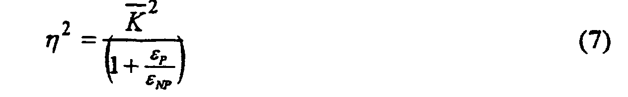
Dans ces équations, εP et εNP sont les constantes diélectriques respectivement du
corps piézoélectrique et du corps non piézoélectrique, e = e15 est un coefficient
du tenseur piézoélectrique et
Pour déterminer les conditions d'existence de ces ondes d'interface, examinons
les trois termes de l'équation (5). Ces termes doivent être réels et positifs, la
vitesse v est donc inférieure ou au plus égale à la plus petite des vitesses vP et
vNP. Si v est égale à vNP ≤ vP, le deuxième terme s'annule et lorsque v décroít, les
deux premiers termes augmentent. η2 doit donc être supérieur au premier terme
lorsque v = vNP.In these equations, ε P and ε NP are the dielectric constants respectively of the piezoelectric body and the non-piezoelectric body, e = e 15 is a coefficient of the piezoelectric tensor and
To determine the conditions of existence of these interface waves, let us examine the three terms of equation (5). These terms must be real and positive, the speed v is therefore less than or at most equal to the smallest of the speeds v P and v NP . If v is equal to v NP ≤ v P , the second term is canceled and when v decreases, the first two terms increase. η 2 must therefore be greater than the first term when v = v NP .
Si la vitesse v est égale à vP ≤ vNP, le premier terme s'annule et lorsque v décroít
les deux premiers termes augmentent η2 doit donc aussi être supérieur au
deuxième terme lorsque v = vP.
Les conditions d'existence sont donc données par le couple d'inégalités
suivantes :
The conditions of existence are therefore given by the following pair of inequalities:
Sur la figure 3, on a tracé pour différentes valeurs de η2 (0,05 ; 0,1 et 0,3) les
deux courbes vNP/vP en fonction de ρNP/ρp qui délimitent le domaine d'existence
de ces ondes, tel que défini par les inégalités (8). On peut y remarquer que ces
ondes existent toujours quelque soit ρNP/ρP, lorsque vNP = vP = vS. Dans ces
conditions leur vitesse v est donnée par :

On peut y remarquer aussi que plus ρNP est petit devant ρP, plus le domaine
d'existence s'élargit à des vitesses vNP supérieures à vP. Par ailleurs, plus η2 sera
grand et plus ρNP sera petit devant ρP, plus les ondes seront localisées près de
l'interface.
Le coefficient de couplage 2Δv/v de ces ondes peut être aisément calculé à partir
de la vitesse vCC lorsque l'interface est court-circuitée, ou de la vitesse vNC
lorsque l'interface n'est pas court-circuitée. Lorsque vNP = vP = vS. On trouve :

The coupling coefficient 2Δv / v of these waves can be easily calculated from the speed v CC when the interface is short-circuited, or from the speed v NC when the interface is not short-circuited. When v NP = v P = v S. We find :
Le coefficient de couplage sera donc d'autant plus grand que
Afin d'aider à la sélection des couples de matériaux pouvant propager ces ondes
d'interface transversales, on a indiqué dans le tableau 1 suivant la vitesse
transversale v d'un certain nombre de matériaux ainsi que leur densité p et leur
constante diélectrique relative ε.
Dans ce tableau, les matériaux 1 à 8 sont piézoélectriques et les matériaux 9 à 12 non piézoélectriques.In this table, materials 1 to 8 are piezoelectric and materials 9 to 12 non piezoelectric.
Pour réaliser un filtre acoustique à l'interface entre un matériau piézoélectrique et un matériau non piézoélectrique, il faut donc :
- choisir une orientation des axes cristallographiques du cristal piézoélectrique telle que selon la direction de propagation choisie, l'onde soit purement transversale ou dont la composante transversale du vecteur déplacement 7 soit dominante et telle que cette onde soit piézoélectriquement couplée,
- choisir une orientation des axes cristallographiques du cristal non piézoélectrique telle que selon la direction de propagation choisie, l'onde soit purement transversale ou dont la composante transversale du vecteur déplacement 7 soit dominante et telle que cette onde ait une vitesse de propagation égale ou supérieure à la vitesse des ondes transversales ou quasi-transversale dans le corps piézoélectrique,
- choisir si possible un cristal non piézoélectrique de densité inférieure à celle du cristal piézoélectrique, et
- choisir si possible un cristal non piézoélectrique de constante diélectrique inférieure à celle du cristal piézoélectrique.
- choosing an orientation of the crystallographic axes of the piezoelectric crystal such that, depending on the direction of propagation chosen, the wave is purely transverse or whose transverse component of the displacement vector 7 is dominant and such that this wave is piezoelectrically coupled,
- choose an orientation of the crystallographic axes of the non-piezoelectric crystal such that, according to the direction of propagation chosen, the wave is purely transverse or whose transverse component of the displacement vector 7 is dominant and such that this wave has a propagation speed equal to or greater than the speed of the transverse or quasi-transverse waves in the piezoelectric body,
- if possible, choose a non-piezoelectric crystal with a density lower than that of the piezoelectric crystal, and
- if possible choose a non-piezoelectric crystal with a dielectric constant lower than that of the piezoelectric crystal.
Pour satisfaire les conditions d'existence d'ondes d'interface quasi-transversales, (Q-SH), on tourne légèrement les cristaux l'un par rapport à l'autre autour d'un axe perpendiculaire à leur interface, depuis les orientations cristallines décrites.To satisfy the conditions of existence of quasi-transverse interface waves, (Q-SH), we turn the crystals slightly relative to each other around a axis perpendicular to their interface, from the crystal orientations described.
Selon une particularité de l'invention, sur la surface de l'un des matériaux, on dépose ou on enterre dans des sillons gravés d'épaisseur contrôlée selon les axes adéquats, la structure métallique du filtre plan, comme représenté sur la figure 2. Ensuite on adhère à cette surface l'autre matériau selon les axes adéquats au moyen de tout procédé envisageable d'adhérence élastique.According to a feature of the invention, on the surface of one of the materials, one deposit or bury in engraved furrows of controlled thickness along the axes the metal structure of the flat filter, as shown in Figure 2. Then the other material is adhered to this surface along the axes suitable for using any conceivable method of elastic adhesion.
A titre d'exemple, on peut adhérer un cristal de YAG non piézoélectrique sur un cristal de Niobate de Lithium (LiNbO3) piézoélectrique ou sur un cristal de Tantalate de Lithium (LiTaO3) piézoélectrique, de coupe suivant l'axe cristallographique Y, la propagation se faisant suivant l'axe cristallographique X.For example, a non-piezoelectric YAG crystal can be adhered to a piezoelectric Lithium Niobate (LiNbO 3 ) crystal or to a piezoelectric Lithium Tantalate (LiTaO 3 ) crystal, cut along the crystallographic axis Y, the propagation taking place along the crystallographic axis X.
Selon une autre variante du filtre selon l'invention, l'un des deux corps 1, 2 est cristallin et l'autre est obtenu par un dépôt ou une épitaxie. Dans ces conditions, à la surface du matériau cristallin, on dépose ou on enterre dans des sillons gravés d'épaisseur contrôlée, selon les axes adéquats, la structure métallique qui compose le filtre plan et on dépose ou on forme par épitaxie le second matériau selon les axes adéquats à la surface ainsi préparée du matériau cristallin.According to another variant of the filter according to the invention, one of the two bodies 1, 2 is crystalline and the other is obtained by deposition or epitaxy. In these conditions, on the surface of the crystalline material, we deposit or bury it in furrows engraved with controlled thickness, along the appropriate axes, the metal structure which composes the flat filter and deposits or forms the second material by epitaxy along the axes appropriate to the surface thus prepared of the crystalline material.
On peut ainsi déposer du silicium amorphe (Si) non piézoélectrique sur une surface ainsi préparée de Niobate de Lithium YX-LiNbO3 piézoélectrique, de coupe Y (où Y est tourné d'un certain angle) la propagation s'effectuant suivant l'axe X. On peut aussi former par épitaxie une couche de Nitrure d'Aluminium (AlN) piézoélectrique sur une surface de Saphir (Al2O3) non piézoélectrique.It is thus possible to deposit non-piezoelectric amorphous silicon (Si) on a surface thus prepared of piezoelectric Lithium Niobate YX-LiNbO 3 , of section Y (where Y is rotated by a certain angle), the propagation taking place along the axis X. A piezoelectric layer of Aluminum Nitride (AlN) can also be formed by epitaxy on a surface of non piezoelectric Sapphire (Al 2 O 3 ).
Claims (15)
- Plane structure acoustic filter in which acoustic waves spread substantially inside a plane,
characterised in that it includes two solid bodies (1, 2), at least one of these being piezoelectric, these bodies being linked to each other so as to have a plane interface (3) between them, the acoustic waves being generated by the piezoelectric body with the aid of an electric field and guided by the interface between the two solid bodies, the latter being selected so that these waves have an acoustic energy these decreases exponentially in the two bodies from the interface in a direction (Oy) perpendicular to the interface, the displacement vector of the atoms of the materials linked to these waves situated in the perpendicular plane to said plane interface (3) separating said two solid bodies (1, 2). - Acoustic filter according to claim 1,
characterised in that the crystallographic axes of the materials constituting the two bodies (1, 2) are selected so as to obtain at the interface (3) transversal acoustic waves (SH) or quasi-transversal waves (Q-SH) whose displacement vector (7) has a single component which is transversal inside the plane of the interface (3) or a dominant transversal component, and when the wave is coupled piezoelectrically. - Acoustic filter according to claim 1 or 2,
characterised in that the two bodies (1, 2) are made of the same piezoelectric material and have the same crystalline orientations so as to form a single solid body inside which a plane metal structure (9, 9', 10) forming the filter serves as a piezoelectric guide for the transversal (SH) or quasi-transversal (Q-SH) interface acoustic waves. - Acoustic filter according to claim 3,
characterised in that the crystallographic axes of the material constituting the two solid bodies are selected so that the transversal component of the displacement vector (7) of the acoustic waves inside the plane of the interface (3) is the sole component of the displacement vector, the material being piezoelectric from the 6 mm hexagonal category whose crystallographic axis C is inside the plane of the interface perpendicular to the direction (Ox) of propagation of the acoustic waves. - Acoustic filter according to claim 3,
characterised in that the crystallographic axes of the material constituting the two bodies (1, 2) are selected so that the transversal component of the displacement vector (7) of the acoustic waves inside the plane of the interface (3) is dominant, the two bodies being obtained by making a cut along the crystallographic axis Y, this axis Y being orientated by a certain angle in lithium niobate (YX-LiNbO3) or lithium tantalate (YX-LiTaO3), the acoustic waves spreading along the crystallographic axis X of the material. - Acoustic filter according to claim 3,
characterised in that the crystallographic axes of the material constituting the two bodies (1, 2) are selected so that the transversal component of the displacement vector (7) of the acoustic waves inside the plane of the interface (3) is dominant, the two bodies being obtained by making cuts along the crystallographic axis ST of the quartz (ST-X quartz), the acoustic waves spreading along the crystallographic axis X of the material. - Acoustic filter according to one of claims 3 to 6,
characterised in that it is obtained from a sole piezoelectric crystal which has been cut along a plane containing the propagation axis (Ox) of the acoustic waves and the axis of the sole transverse (SH) or dominant (Q-SH) displacement vector (7) of the selected transversal or quasi-transversal interface acoustic waves, the surface obtained by the cut of one of the portions of the cut crystal including etched grooves with a controlled thickness in which a plane metal filter structure (9, 9', 10) is formed, the two cut portions (1, 2) having been replaced by each other along the same crystalline orientations and fixed to each other by an elastic adherence element. - Acoustic filter according to claim 1 or 2,
characterised in that one (1) of the bodies (1, 2) is piezoelectric and the other (2) is non-piezoelectric, the materials constituting the bodies (1, 2) being selected so that the speed of propagation of the transversal or quasi-transversal acoustic waves inside a plane parallel to the interface plane (3) in the non-piezoelectric material is equal to or greater than that in the piezoelectric material. - Acoustic filter according to claim 8,
characterised in that the dielectric constant and density of the non-piezoelectric material are less than the dielectric constant and density of the piezoelectric material. - Acoustic filter according to claim 8 or 9,
characterised in that so as to satisfy the conditions of existence of the interface acoustic waves (Q-SH) for which the transversal component of the displacement vector (7) inside the plane of the interface is dominant, the crystal of one of the two bodies (1, 2) is orientated slightly with respect to the other around an axis perpendicular the plane of their interface (3) from the crystalline orientations required so that the piezoelectric waves are purely transversal (SH) at the interface (3) between the two bodies (1, 2). - Acoustic filter according to one of claims 8 to 10,
characterised in that the two bodies (1, 2) are obtained from the cut of two crystalline materials (A, B) along suitable crystallographic axes, the surface of one of the materials forming said interface (3) including a plane metal filter structure (9, 9', 10), the two bodies being fixed to each other along suitable axes by means of an elastic adherence method. - Acoustic filter according to one of claims 8 to 11,
characterised in that the non-piezoelectric body (2) is a YAG crystal, whereas the piezoelectric body (1) is a lithium niobate crystal (YX-LiNbO3) or a lithium tantalate crystal (YX-LiTaO3), with a cut along the crystallographic axis Y, propagation being effected along the crystallographic axis X, the two bodies being fixed to each other along the suitable axes by means of any elastic adherence method. - Acoustic filter according to one of claims 8 to 11,
characterised in that it is formed by a crystalline material having a surface including a plane metallic filter structure, the other body being formed on this surface by a deposit or epitaxial growth along the suitable axes. - Acoustic filter according to claim 13,
characterised in that it is embodied by a deposit of amorphous silicon on a surface of lithium niobate (YX-LiNbO3) with a cut along the crystallographic axis Y where Y is orientated by a certain angle, propagation of the acoustic waves being effected along the crystallographic axis X. - Acoustic filter according to claim 13,
characterised in that it is embodied by an epitaxial growth of a film of aluminium nitride (AlN) on a sapphire surface (Al2O3).
Applications Claiming Priority (3)
| Application Number | Priority Date | Filing Date | Title |
|---|---|---|---|
| FR9912992 | 1999-10-15 | ||
| FR9912992A FR2799906B1 (en) | 1999-10-15 | 1999-10-15 | INTERFACE ACOUSTIC WAVE FILTER, PARTICULARLY FOR WIRELESS LINKS |
| PCT/FR2000/002727 WO2001029964A1 (en) | 1999-10-15 | 2000-09-28 | Interface acoustic wave filter, especially for wireless connections |
Publications (2)
| Publication Number | Publication Date |
|---|---|
| EP1222735A1 EP1222735A1 (en) | 2002-07-17 |
| EP1222735B1 true EP1222735B1 (en) | 2004-02-25 |
Family
ID=9551074
Family Applications (1)
| Application Number | Title | Priority Date | Filing Date |
|---|---|---|---|
| EP00966253A Revoked EP1222735B1 (en) | 1999-10-15 | 2000-09-28 | Interface acoustic wave filter, especially for wireless connections |
Country Status (7)
| Country | Link |
|---|---|
| US (1) | US6737941B1 (en) |
| EP (1) | EP1222735B1 (en) |
| JP (1) | JP4820037B2 (en) |
| AT (1) | ATE260516T1 (en) |
| DE (1) | DE60008569T9 (en) |
| FR (1) | FR2799906B1 (en) |
| WO (1) | WO2001029964A1 (en) |
Families Citing this family (24)
| Publication number | Priority date | Publication date | Assignee | Title |
|---|---|---|---|---|
| FR2799906B1 (en) * | 1999-10-15 | 2002-01-25 | Pierre Tournois | INTERFACE ACOUSTIC WAVE FILTER, PARTICULARLY FOR WIRELESS LINKS |
| FR2837636B1 (en) * | 2002-03-19 | 2004-09-24 | Thales Sa | LITHIUM TANTALATE INTERFACE ACOUSTIC WAVE DEVICE |
| JP3815424B2 (en) * | 2002-11-08 | 2006-08-30 | 株式会社村田製作所 | Boundary acoustic wave device |
| KR100766263B1 (en) | 2003-02-10 | 2007-10-15 | 가부시키가이샤 무라타 세이사쿠쇼 | Elastic boundary wave device |
| US7453184B2 (en) * | 2003-04-18 | 2008-11-18 | Murata Manufacturing Co., Ltd. | Boundary acoustic wave device |
| DE10325281B4 (en) * | 2003-06-04 | 2018-05-17 | Snaptrack, Inc. | Electroacoustic component and method of manufacture |
| KR100850861B1 (en) * | 2004-01-19 | 2008-08-06 | 가부시키가이샤 무라타 세이사쿠쇼 | Acoustic boundary wave device |
| CN100576733C (en) * | 2004-03-05 | 2009-12-30 | 株式会社村田制作所 | Boundary acoustic wave device |
| WO2005099091A1 (en) * | 2004-04-08 | 2005-10-20 | Murata Manufacturing Co., Ltd. | Elastic boundary wave filter |
| WO2006011417A1 (en) * | 2004-07-26 | 2006-02-02 | Murata Manufacturing Co., Ltd. | Surface acoustic wave device |
| JP2006203304A (en) * | 2005-01-18 | 2006-08-03 | Hitachi Media Electoronics Co Ltd | Piezoelectric thin-film resonator, oscillator using the same, and semiconductor integrated circuit containing the same |
| US7619347B1 (en) | 2005-05-24 | 2009-11-17 | Rf Micro Devices, Inc. | Layer acoustic wave device and method of making the same |
| WO2007007462A1 (en) * | 2005-07-14 | 2007-01-18 | Murata Manufacturing Co., Ltd. | Elastic boundary wave device and method of manufacturing the same |
| JP4001157B2 (en) * | 2005-07-22 | 2007-10-31 | 株式会社村田製作所 | Boundary acoustic wave device |
| DE102005055871A1 (en) | 2005-11-23 | 2007-05-24 | Epcos Ag | Guided bulk acoustic wave operated component for e.g. ladder filter, has dielectric layer with low acoustic impedance, and metal layer including partial layer with high impedance, where ratio between impedances lies in certain range |
| DE102005055870A1 (en) | 2005-11-23 | 2007-05-24 | Epcos Ag | Electroacoustic component, has layer system arranged between carrier substrate and piezo substrate, and comprising metal layer and dielectric layer, where thickness of piezo substrate is maximally half of thickness of carrier substrate |
| CN101454974B (en) * | 2006-05-30 | 2012-05-30 | 株式会社村田制作所 | Boundary acoustic wave device |
| JP4760911B2 (en) * | 2006-09-21 | 2011-08-31 | 株式会社村田製作所 | Boundary acoustic wave device |
| WO2008044411A1 (en) * | 2006-10-12 | 2008-04-17 | Murata Manufacturing Co., Ltd. | Elastic boundary-wave device |
| US8490260B1 (en) | 2007-01-17 | 2013-07-23 | Rf Micro Devices, Inc. | Method of manufacturing SAW device substrates |
| US7408286B1 (en) * | 2007-01-17 | 2008-08-05 | Rf Micro Devices, Inc. | Piezoelectric substrate for a saw device |
| CN102057571B (en) | 2008-06-06 | 2014-03-19 | 松下电器产业株式会社 | Acoustic wave duplexer |
| US20110133858A1 (en) * | 2008-08-07 | 2011-06-09 | Goto Rei | Elastic wave element and electronic device using the same |
| TW202401007A (en) * | 2022-03-14 | 2024-01-01 | 日商蓋亞尼克斯股份有限公司 | Component, electronic device, electronic equipment, and system |
Family Cites Families (8)
| Publication number | Priority date | Publication date | Assignee | Title |
|---|---|---|---|---|
| FR2145750A5 (en) * | 1971-07-09 | 1973-02-23 | Thomson Csf | |
| US4328472A (en) * | 1980-11-03 | 1982-05-04 | United Technologies Corporation | Acoustic guided wave devices |
| US4484098A (en) * | 1983-12-19 | 1984-11-20 | United Technologies Corporation | Environmentally stable lithium niobate acoustic wave devices |
| US5633616A (en) * | 1994-10-07 | 1997-05-27 | Mitsubishi Denki Kabushiki Kaisha | Thin film saw filter including doped electrodes |
| JPH09107264A (en) * | 1995-10-11 | 1997-04-22 | Toyo Commun Equip Co Ltd | Channel wave local confinement type piezoelectric oscillator and filter |
| US6046656A (en) * | 1997-05-08 | 2000-04-04 | Kabushiki Kaisha Toshiba | Elastic boundary wave device and method of its manufacture |
| WO1998052279A1 (en) * | 1997-05-12 | 1998-11-19 | Hitachi, Ltd. | Elastic wave device |
| FR2799906B1 (en) * | 1999-10-15 | 2002-01-25 | Pierre Tournois | INTERFACE ACOUSTIC WAVE FILTER, PARTICULARLY FOR WIRELESS LINKS |
-
1999
- 1999-10-15 FR FR9912992A patent/FR2799906B1/en not_active Expired - Lifetime
-
2000
- 2000-09-28 US US10/110,403 patent/US6737941B1/en not_active Expired - Lifetime
- 2000-09-28 EP EP00966253A patent/EP1222735B1/en not_active Revoked
- 2000-09-28 JP JP2001531203A patent/JP4820037B2/en not_active Expired - Fee Related
- 2000-09-28 DE DE60008569T patent/DE60008569T9/en active Active
- 2000-09-28 WO PCT/FR2000/002727 patent/WO2001029964A1/en active IP Right Grant
- 2000-09-28 AT AT00966253T patent/ATE260516T1/en not_active IP Right Cessation
Also Published As
| Publication number | Publication date |
|---|---|
| US6737941B1 (en) | 2004-05-18 |
| JP4820037B2 (en) | 2011-11-24 |
| DE60008569D1 (en) | 2004-04-01 |
| ATE260516T1 (en) | 2004-03-15 |
| WO2001029964A1 (en) | 2001-04-26 |
| JP2003512637A (en) | 2003-04-02 |
| EP1222735A1 (en) | 2002-07-17 |
| FR2799906A1 (en) | 2001-04-20 |
| FR2799906B1 (en) | 2002-01-25 |
| DE60008569T9 (en) | 2005-04-07 |
| DE60008569T2 (en) | 2004-12-16 |
Similar Documents
| Publication | Publication Date | Title |
|---|---|---|
| EP1222735B1 (en) | Interface acoustic wave filter, especially for wireless connections | |
| CA2553861C (en) | Hybrid resonant structure | |
| JP5193051B2 (en) | Electroacoustic element | |
| EP3113362B1 (en) | Device with elastic surface waves comprising a single-crystal piezoelectric film and a crystalline substrate, with low viscoelastic coefficients | |
| EP2909932B1 (en) | Transducer with bulk waves surface-guided by synchronous excitation structures | |
| EP2301150B1 (en) | Hbar resonator with increased temperature stability | |
| EP2351214B1 (en) | Transversally coupled filter elements on bulk acoustic wave resonance structures with multiple harmonic resonances. | |
| EP2665999B1 (en) | Temperature sensor comprising a high-overtone bulk acoustic resonator | |
| FR2785473A1 (en) | LOW ACOUSTIC SURFACE WAVE LOW FILTER ON OPTIMIZED CUTTER QUARTZ SUBSTRATE | |
| EP2291911B1 (en) | Hbar resonator with a high level of integration | |
| EP1500191B1 (en) | Device with interface sound waves made of lithium tantalate | |
| EP0116800B1 (en) | Excitable piezoelectric epitaxial structure and electronic device for the generation of surface acoustic waves therein | |
| EP0369835B1 (en) | Interdigital transducer for an saw filter | |
| WO2014079912A1 (en) | Surface acoustic wave transducer of which the waves propagate on a lithium niobate or lithium tantalate substrate | |
| EP3032742B1 (en) | Surface acoustic wave sensor that can be polled remotely | |
| WO2004102796A1 (en) | Integrated resonators and time base incorporating said resonators | |
| WO2022063231A1 (en) | Surface acoustic wave devices with ultra-thin transducers | |
| FR3135868A1 (en) | SURFACE ACOUSTIC WAVE DEVICE INTEGRATING A THIN LAYER OF METALLIC MATERIAL |
Legal Events
| Date | Code | Title | Description |
|---|---|---|---|
| PUAI | Public reference made under article 153(3) epc to a published international application that has entered the european phase |
Free format text: ORIGINAL CODE: 0009012 |
|
| 17P | Request for examination filed |
Effective date: 20020412 |
|
| AK | Designated contracting states |
Kind code of ref document: A1 Designated state(s): AT BE CH CY DE DK ES FI FR GB GR IE IT LI LU MC NL PT SE |
|
| AX | Request for extension of the european patent |
Free format text: AL;LT;LV;MK;RO;SI |
|
| 17Q | First examination report despatched |
Effective date: 20021219 |
|
| GRAP | Despatch of communication of intention to grant a patent |
Free format text: ORIGINAL CODE: EPIDOSNIGR1 |
|
| GRAS | Grant fee paid |
Free format text: ORIGINAL CODE: EPIDOSNIGR3 |
|
| GRAA | (expected) grant |
Free format text: ORIGINAL CODE: 0009210 |
|
| AK | Designated contracting states |
Kind code of ref document: B1 Designated state(s): AT BE CH CY DE DK ES FI FR GB GR IE IT LI LU MC NL PT SE |
|
| PG25 | Lapsed in a contracting state [announced via postgrant information from national office to epo] |
Ref country code: IT Free format text: LAPSE BECAUSE OF FAILURE TO SUBMIT A TRANSLATION OF THE DESCRIPTION OR TO PAY THE FEE WITHIN THE PRESCRIBED TIME-LIMIT;WARNING: LAPSES OF ITALIAN PATENTS WITH EFFECTIVE DATE BEFORE 2007 MAY HAVE OCCURRED AT ANY TIME BEFORE 2007. THE CORRECT EFFECTIVE DATE MAY BE DIFFERENT FROM THE ONE RECORDED. Effective date: 20040225 Ref country code: FI Free format text: LAPSE BECAUSE OF FAILURE TO SUBMIT A TRANSLATION OF THE DESCRIPTION OR TO PAY THE FEE WITHIN THE PRESCRIBED TIME-LIMIT Effective date: 20040225 Ref country code: CY Free format text: LAPSE BECAUSE OF FAILURE TO SUBMIT A TRANSLATION OF THE DESCRIPTION OR TO PAY THE FEE WITHIN THE PRESCRIBED TIME-LIMIT Effective date: 20040225 Ref country code: GB Free format text: LAPSE BECAUSE OF FAILURE TO SUBMIT A TRANSLATION OF THE DESCRIPTION OR TO PAY THE FEE WITHIN THE PRESCRIBED TIME-LIMIT Effective date: 20040225 Ref country code: NL Free format text: LAPSE BECAUSE OF FAILURE TO SUBMIT A TRANSLATION OF THE DESCRIPTION OR TO PAY THE FEE WITHIN THE PRESCRIBED TIME-LIMIT Effective date: 20040225 Ref country code: AT Free format text: LAPSE BECAUSE OF FAILURE TO SUBMIT A TRANSLATION OF THE DESCRIPTION OR TO PAY THE FEE WITHIN THE PRESCRIBED TIME-LIMIT Effective date: 20040225 Ref country code: IE Free format text: LAPSE BECAUSE OF FAILURE TO SUBMIT A TRANSLATION OF THE DESCRIPTION OR TO PAY THE FEE WITHIN THE PRESCRIBED TIME-LIMIT Effective date: 20040225 |
|
| REG | Reference to a national code |
Ref country code: GB Ref legal event code: FG4D Free format text: NOT ENGLISH |
|
| REG | Reference to a national code |
Ref country code: CH Ref legal event code: EP |
|
| REG | Reference to a national code |
Ref country code: IE Ref legal event code: FG4D Free format text: FRENCH |
|
| REF | Corresponds to: |
Ref document number: 60008569 Country of ref document: DE Date of ref document: 20040401 Kind code of ref document: P |
|
| REG | Reference to a national code |
Ref country code: CH Ref legal event code: NV Representative=s name: BUGNION S.A. |
|
| PG25 | Lapsed in a contracting state [announced via postgrant information from national office to epo] |
Ref country code: DK Free format text: LAPSE BECAUSE OF FAILURE TO SUBMIT A TRANSLATION OF THE DESCRIPTION OR TO PAY THE FEE WITHIN THE PRESCRIBED TIME-LIMIT Effective date: 20040525 Ref country code: GR Free format text: LAPSE BECAUSE OF FAILURE TO SUBMIT A TRANSLATION OF THE DESCRIPTION OR TO PAY THE FEE WITHIN THE PRESCRIBED TIME-LIMIT Effective date: 20040525 Ref country code: SE Free format text: LAPSE BECAUSE OF FAILURE TO SUBMIT A TRANSLATION OF THE DESCRIPTION OR TO PAY THE FEE WITHIN THE PRESCRIBED TIME-LIMIT Effective date: 20040525 |
|
| PG25 | Lapsed in a contracting state [announced via postgrant information from national office to epo] |
Ref country code: ES Free format text: LAPSE BECAUSE OF FAILURE TO SUBMIT A TRANSLATION OF THE DESCRIPTION OR TO PAY THE FEE WITHIN THE PRESCRIBED TIME-LIMIT Effective date: 20040605 |
|
| NLV1 | Nl: lapsed or annulled due to failure to fulfill the requirements of art. 29p and 29m of the patents act | ||
| GBV | Gb: ep patent (uk) treated as always having been void in accordance with gb section 77(7)/1977 [no translation filed] |
Effective date: 20040225 |
|
| LTIE | Lt: invalidation of european patent or patent extension |
Effective date: 20040225 |
|
| REG | Reference to a national code |
Ref country code: IE Ref legal event code: FD4D |
|
| PG25 | Lapsed in a contracting state [announced via postgrant information from national office to epo] |
Ref country code: LU Free format text: LAPSE BECAUSE OF NON-PAYMENT OF DUE FEES Effective date: 20040928 |
|
| PG25 | Lapsed in a contracting state [announced via postgrant information from national office to epo] |
Ref country code: BE Free format text: LAPSE BECAUSE OF NON-PAYMENT OF DUE FEES Effective date: 20040930 Ref country code: MC Free format text: LAPSE BECAUSE OF NON-PAYMENT OF DUE FEES Effective date: 20040930 |
|
| PLBI | Opposition filed |
Free format text: ORIGINAL CODE: 0009260 |
|
| PLAX | Notice of opposition and request to file observation + time limit sent |
Free format text: ORIGINAL CODE: EPIDOSNOBS2 |
|
| 26 | Opposition filed |
Opponent name: DR. TAM AXEL VON BUELOW Effective date: 20041123 |
|
| BERE | Be: lapsed |
Owner name: *TOURNOIS PIERRE Effective date: 20040930 |
|
| PLAX | Notice of opposition and request to file observation + time limit sent |
Free format text: ORIGINAL CODE: EPIDOSNOBS2 |
|
| PLBB | Reply of patent proprietor to notice(s) of opposition received |
Free format text: ORIGINAL CODE: EPIDOSNOBS3 |
|
| BERE | Be: lapsed |
Owner name: *TOURNOIS PIERRE Effective date: 20040930 |
|
| PG25 | Lapsed in a contracting state [announced via postgrant information from national office to epo] |
Ref country code: PT Free format text: LAPSE BECAUSE OF NON-PAYMENT OF DUE FEES Effective date: 20040725 |
|
| PGFP | Annual fee paid to national office [announced via postgrant information from national office to epo] |
Ref country code: CH Payment date: 20080930 Year of fee payment: 9 |
|
| PLAB | Opposition data, opponent's data or that of the opponent's representative modified |
Free format text: ORIGINAL CODE: 0009299OPPO |
|
| REG | Reference to a national code |
Ref country code: CH Ref legal event code: PL |
|
| PG25 | Lapsed in a contracting state [announced via postgrant information from national office to epo] |
Ref country code: LI Free format text: LAPSE BECAUSE OF NON-PAYMENT OF DUE FEES Effective date: 20090930 Ref country code: CH Free format text: LAPSE BECAUSE OF NON-PAYMENT OF DUE FEES Effective date: 20090930 |
|
| PLAY | Examination report in opposition despatched + time limit |
Free format text: ORIGINAL CODE: EPIDOSNORE2 |
|
| PLBC | Reply to examination report in opposition received |
Free format text: ORIGINAL CODE: EPIDOSNORE3 |
|
| REG | Reference to a national code |
Ref country code: FR Ref legal event code: ST Effective date: 20110531 |
|
| PG25 | Lapsed in a contracting state [announced via postgrant information from national office to epo] |
Ref country code: FR Free format text: LAPSE BECAUSE OF NON-PAYMENT OF DUE FEES Effective date: 20100930 |
|
| PGFP | Annual fee paid to national office [announced via postgrant information from national office to epo] |
Ref country code: FR Payment date: 20091006 Year of fee payment: 10 |
|
| RDAF | Communication despatched that patent is revoked |
Free format text: ORIGINAL CODE: EPIDOSNREV1 |
|
| REG | Reference to a national code |
Ref country code: DE Ref legal event code: R064 Ref document number: 60008569 Country of ref document: DE Ref country code: DE Ref legal event code: R103 Ref document number: 60008569 Country of ref document: DE |
|
| APBM | Appeal reference recorded |
Free format text: ORIGINAL CODE: EPIDOSNREFNO |
|
| APBP | Date of receipt of notice of appeal recorded |
Free format text: ORIGINAL CODE: EPIDOSNNOA2O |
|
| APAH | Appeal reference modified |
Free format text: ORIGINAL CODE: EPIDOSCREFNO |
|
| APBQ | Date of receipt of statement of grounds of appeal recorded |
Free format text: ORIGINAL CODE: EPIDOSNNOA3O |
|
| PGFP | Annual fee paid to national office [announced via postgrant information from national office to epo] |
Ref country code: DE Payment date: 20160926 Year of fee payment: 17 |
|
| APBU | Appeal procedure closed |
Free format text: ORIGINAL CODE: EPIDOSNNOA9O |
|
| RAP2 | Party data changed (patent owner data changed or rights of a patent transferred) |
Owner name: EPCOS AG |
|
| RIN2 | Information on inventor provided after grant (corrected) |
Inventor name: EPCOS AG |
|
| RDAG | Patent revoked |
Free format text: ORIGINAL CODE: 0009271 |
|
| STAA | Information on the status of an ep patent application or granted ep patent |
Free format text: STATUS: PATENT REVOKED |
|
| 27W | Patent revoked |
Effective date: 20130309 |