EP1221761A1 - Method for controlling neutral point potential of inverter of neutral point clamping type - Google Patents
Method for controlling neutral point potential of inverter of neutral point clamping type Download PDFInfo
- Publication number
- EP1221761A1 EP1221761A1 EP00951922A EP00951922A EP1221761A1 EP 1221761 A1 EP1221761 A1 EP 1221761A1 EP 00951922 A EP00951922 A EP 00951922A EP 00951922 A EP00951922 A EP 00951922A EP 1221761 A1 EP1221761 A1 EP 1221761A1
- Authority
- EP
- European Patent Office
- Prior art keywords
- vector
- phase
- inverter
- voltage
- neutral point
- Prior art date
- Legal status (The legal status is an assumption and is not a legal conclusion. Google has not performed a legal analysis and makes no representation as to the accuracy of the status listed.)
- Granted
Links
Images




Classifications
-
- H—ELECTRICITY
- H02—GENERATION; CONVERSION OR DISTRIBUTION OF ELECTRIC POWER
- H02M—APPARATUS FOR CONVERSION BETWEEN AC AND AC, BETWEEN AC AND DC, OR BETWEEN DC AND DC, AND FOR USE WITH MAINS OR SIMILAR POWER SUPPLY SYSTEMS; CONVERSION OF DC OR AC INPUT POWER INTO SURGE OUTPUT POWER; CONTROL OR REGULATION THEREOF
- H02M7/00—Conversion of AC power input into DC power output; Conversion of DC power input into AC power output
- H02M7/42—Conversion of DC power input into AC power output without possibility of reversal
- H02M7/44—Conversion of DC power input into AC power output without possibility of reversal by static converters
- H02M7/48—Conversion of DC power input into AC power output without possibility of reversal by static converters using discharge tubes with control electrode or semiconductor devices with control electrode
- H02M7/483—Converters with outputs that each can have more than two voltages levels
- H02M7/487—Neutral point clamped inverters
-
- H—ELECTRICITY
- H02—GENERATION; CONVERSION OR DISTRIBUTION OF ELECTRIC POWER
- H02M—APPARATUS FOR CONVERSION BETWEEN AC AND AC, BETWEEN AC AND DC, OR BETWEEN DC AND DC, AND FOR USE WITH MAINS OR SIMILAR POWER SUPPLY SYSTEMS; CONVERSION OF DC OR AC INPUT POWER INTO SURGE OUTPUT POWER; CONTROL OR REGULATION THEREOF
- H02M7/00—Conversion of AC power input into DC power output; Conversion of DC power input into AC power output
- H02M7/42—Conversion of DC power input into AC power output without possibility of reversal
- H02M7/44—Conversion of DC power input into AC power output without possibility of reversal by static converters
- H02M7/48—Conversion of DC power input into AC power output without possibility of reversal by static converters using discharge tubes with control electrode or semiconductor devices with control electrode
-
- H—ELECTRICITY
- H02—GENERATION; CONVERSION OR DISTRIBUTION OF ELECTRIC POWER
- H02M—APPARATUS FOR CONVERSION BETWEEN AC AND AC, BETWEEN AC AND DC, OR BETWEEN DC AND DC, AND FOR USE WITH MAINS OR SIMILAR POWER SUPPLY SYSTEMS; CONVERSION OF DC OR AC INPUT POWER INTO SURGE OUTPUT POWER; CONTROL OR REGULATION THEREOF
- H02M7/00—Conversion of AC power input into DC power output; Conversion of DC power input into AC power output
- H02M7/42—Conversion of DC power input into AC power output without possibility of reversal
- H02M7/44—Conversion of DC power input into AC power output without possibility of reversal by static converters
- H02M7/48—Conversion of DC power input into AC power output without possibility of reversal by static converters using discharge tubes with control electrode or semiconductor devices with control electrode
- H02M7/483—Converters with outputs that each can have more than two voltages levels
- H02M7/4833—Capacitor voltage balancing
Definitions
- the present invention relates to a neutral point potential control method of a power conversion device, such as a three-phase neutral point clamp type inverter, for performing variable speed driving of a motor or system interconnection, and a power conversion device, such as an inverter servo drive, for performing variable speed driving of a motor, or a power conversion device for performing system interconnection.
- a power conversion device such as a three-phase neutral point clamp type inverter
- a power conversion device such as an inverter servo drive
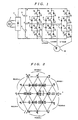
- FIG. 1 shows a basic structure of a three-phase neutral point clamp type inverter, and in the drawing, reference numeral 1 designates a three-phase AC power source; 2, a rectifying element; 3, 4, smoothing capacitors; 6 to 23, diodes; 24 to 35, IGBTs; and 36, a motor.
- Vcn when a potential difference between a neutral point voltage (voltage of a connection point O of serial-connected smoothing capacitors of the inverter) and a negative bus voltage is Vcn, in the neutral point potential control, Vcn must be controlled to be a half voltage of a bus voltage Vpn of the inverter.
- FIG. 1 selects an output vector shown in FIG. 2 and controls Vcn, as voltage vectors which can be used for control of Vcn, there are only twelve vector of xp(1), xn(1), xp(2), xn(2), xp(3), xn(3), yp(1), yn(1), yp(2), yn(2), yp(3), and yn(3).
- FIG. 3 shows connection states of a load and the smoothing capacitors of the inverter in the case where the twelve vectors are outputted.
- Vcn can be controlled.
- a first problem to be solved by the present invention is to provide a neutral point potential control method of a three-phase neutral point clamp type inverter in which without degrading the quality of an inter-phase output voltage, neutral point potential control can be carried out irrespective of a power factor by simple measurement or prediction of a phase current, and neutral point potential fluctuation due to load current unbalance at the time of load ground fault can also be suppressed, whereby the quality, stability and safety of the inverter can be improved.
- FIG. 5 is a vector diagram in which output voltage vectors of a three-phase neutral point clamp type inverter are shown on a plane.
- the three-phase neutral point clamp type PWM inverter outputs a certain voltage vector A in the regions shown in FIG. 5, vectors in a switch state nearest to the tip of the voltage vector are used, these vectors are successively generated, and a pulse width modulation (PWM) is performed so that a composite value of the vectors in a unit time becomes equal to the voltage vector A and the output voltage is obtained.
- PWM pulse width modulation
- reference numeral 1 designates a three-phase AC power source; 2, a rectifying diode bridge; 6 to 11, clamp diodes; 12 to 23, reflux diodes; 24 to 35, IGBTs; 36 to 38, current sensors; and 39, a load motor.
- the neutral line 0 is connected as shown in FIGS. 7 and 8 according to the PWM inverter output load (the load motor 39) and a switch state of the PWM inverter.
- the potential of the neutral line (neutral point potential) is changed by a current for charging the capacitor from the positive bus/negative bus and a current from the connected load.
- switch states shown in FIG. 7 a set of switch states in which although line-to-line voltages outputted to the load are the same, load phases connected to the neutral line are different (adjacent switch states in FIG. 7 are made a set), is used, and a time ratio of generation of the switch states of this set is adjusted, so that the neutral point potential can be finely controlled.
- a zero-phase voltage is added to a percent modulation, and generation times of the switch states of the set shown in FIG. 7 are adjusted, so that the neutral point potential fluctuation is controlled without changing the line-to-line output voltage supplied to the load.
- a voltage vector to be outputted is outputted so as to use the set of the switch states shown in FIG. 7, and the generation times of the switch states of the set are adjusted so that the neutral point potential is controlled.
- the neutral point potential fluctuation at the time of the switch state of FIG. 8 is determined by the phase current of the load connected to the neutral line from FIG. 8.
- the generation time ratio of the switch state shown in FIG. 8 becomes higher than that of the switch state shown in FIG. 7, and in an excessive modulation state in which the percent modulation exceeds about 1.15, there has been a problem that the generation time ratio of the switch state shown in FIG. 7 becomes completely zero, and the fluctuation of the neutral point potential caused by the switch state shown in FIG. 8 can not be suppressed.
- a second problem to be solved by the present invention is to suppress the neutral point potential fluctuation of the three-phase neutral point clamp type inverter, to enable adjustment of the neutral point potential at the time of excessive modulation, which has been conventionally impossible, and to realize the improvement of safety and the improvement of output voltage quality.
- a neutral point potential control method of a neutral point clamp type inverter of the present invention is
- the neutral point potential control method of the three-phase neutral point clamp type inverter as described in (1) and (2) the neutral point potential control becomes possible irrespective of the load power factor, and the control becomes simple since the direction of the load current is merely detected.
- the neutral point potential control of the three-phase neutral point clamp type inverter as described in (3) it is possible to suppress an abrupt neutral point potential fluctuation in a case where the inverter output is grounded, and the stability is improved.
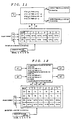
- FIG. 10 shows a control block of the embodiment 1.
- the direction of a current flowing to the neutral point current can be adjusted according to the judgement of the positive or negative of the phase current, and the neutral point potential can be obtained in which when ⁇ is made large irrespective of the load power factor, Vcn rises, and when ⁇ is made small, Vcn drops.
- the embodiment 1 in which the direction of a current of only one phase is measured is modified such that the direction of the sum of current values of two phases is measured as in table 2.
- FIG. 11 shows a control block of the embodiment 2.
- the neutral point potential control method of the neutral point clamp type inverter of the present invention when used, it becomes possible to carry out the neutral point potential control irrespective of the power factor by the simple method in which the direction of the load current is measured or predicted, and the stability and safety of the inverter is remarkably improved. Besides, the neutral point potential fluctuation due to the load current unbalance at the time of the load ground fault can be suppressed, and the safety is further improved.
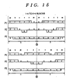
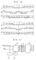
- FIGS. 13 to 16 are examples of PWM output pulse trains of the present invention.
- FIGS. 13 to 16 the illustration is made such that a period of a PWM output is 2 x T, the horizontal axis is made a time series, and a pulse is outputted in order from the left to the right.
- a transfer can be made by the change of the switch state of only one phase from the z vector, and the a or b vector not included in the three adjacent vectors is also outputted.
- Example 1 yp ⁇ b ⁇ z ⁇ yn ⁇ xn ⁇ a ⁇ z ⁇ xp ⁇ yp 1-2 to 6-2 regions (FIG. 14)
- Example 2 xp ⁇ z ⁇ b ⁇ z ⁇ a ⁇ xn, xn ⁇ a ⁇ z ⁇ b ⁇ z ⁇ xp
- Example 3 b ⁇ z ⁇ xp ⁇ a ⁇ xn, xn ⁇ a ⁇ xp ⁇ z ⁇ b 1-4 to 6-4 regions (FIG. 15)
- the generation time (T2) of the z vector shown in FIG. 8 can be determined to be an arbitrary value not less than zero, and the fluctuation of the neutral point potential due to the z vector can be suppressed by shortening T2, and in the case where the percent modulation is large (in the case where the generation times of the x and y vectors become short), the generation time of the z vector which changes the neutral point potential can be made short, so that it is possible to suppress the neutral point potential fluctuation fluctuating at a speed three times as fast as the output frequency.
- the PWM pulse trains of the present invention as described above are adopted, since the switch state of only one phase is changed at the transfer of the PWM pulse, the fluctuation width of the output line-to-line voltage becomes almost equal to the neutral point potential, and a load surge can be suppressed.
- the above PWM pulse trains are examples, and there is a pulse train other than the above examples, which satisfies the feature of the present invention.
- FIG. 17 is a block diagram showing an example of the present invention.
- reference numeral 101 designates a z vector generation time computing unit 1; 102, a z vector generation time upper limit setting unit; 103, a PWM generation time computing unit; 104, a respective vector generation time setting unit; and 105, a PWM pattern generator.
- the generation time of the z vector is greatly changed by the percent modulation, in the case where the percent modulation is small and the generation time of the z vector is also small, when the generation time of the z vector is further shortened, the generation time of both the z vector and the a or b vector to be outputted to compensate the z vector become minute, and in the case where the response of a switch element is slow, a correct pulse can not be outputted, and there is a case where the output voltage becomes insufficient. Then, as shown in FIG.
- the structure is adopted in which the z vector generation time computing unit 1 (101) for changing the set value of T2 in accordance with the percent modulation is added, and the set value of T2 is optimized in accordance with the percent modulation to make an adjust so that the generation of each of the z, a and b vectors does not become too short and the output voltage does not become insufficient.
- FIG. 18 is a block diagram showing an example of the present invention.
- reference numeral 106 designates a z vector generation time computing unit 2.
- the fluctuation direction of the neutral point potential when the z vector is generated is determined according to the direction of the load current of the phase connected to the neutral line, and when the current flows to the neutral line, the neutral point potential becomes high, and when the current flows out, the neutral point potential becomes low.
- a circuit of a structure shown in FIG. 18 is used and the percent modulation and phase of a voltage vector and the direction of a phase current of a load connected to the neutral line are measured by the current sensors 36, 37 and 38 shown in FIG. 6, and in accordance with the current direction and neutral point potential control instructions, an operation of time setting of T2 is carried out by the z vector generation time computing unit 2 (106).
- the neutral point potential fluctuation of the three-phase neutral point clamp type PWM inverter device is suppressed, and further, the adjustment of the neutral point potential at the time of the excessive modulation, which was conventionally impossible, becomes possible, and the improvement of safety and the improvement of output voltage quality can be realized.
- the present invention can be applied to an inverter for carrying out variable speed driving of a motor.
Landscapes
- Engineering & Computer Science (AREA)
- Power Engineering (AREA)
- Inverter Devices (AREA)
Abstract
Description
in an electrical driving state,
when α is made large, Vcn rises,
when α is made small, Vcn drops,
besides, in a regenerative state,
when α is made large, Vcn drops,
when α is made small, Vcn rises,
whereby, the neutral point potential can be controlled by adjusting α.
- regions surrounded by the zero vector, the x vector and the y vector are 1-1 to 6-1,
- regions surrounded by the x vector, the a vector and the z vector are 1-2 to 6-2,
- regions surrounded by the x vector, the y vector and the z vector are 1-3 to 6-3, and
- regions surrounded by the y vector, the b vector and the z vector are 1-4 to 6-4.
if |lu| < |lv+lw|, then generation of the vector xp(1) is suppressed,
if |lu > |lv+lw|, then generation of the vector xn(1) is suppressed,
if |lv| < |lu+lw|, then generation of the vector xp(2) is suppressed,
if |lv| > |lu+lw|, then generation of the vector xn(2) is suppressed,
if |lw| < |lu+lv|, then generation of the vector xp(3) is suppressed,
if |lw| > |lu + lv|, then generation of the vector xn(3) is suppressed,
if |lw | < |lu+lv|, then generation of the vector yn(1) is suppressed,
if |lw > |lu+lv|, then generation of the vector yp(1) is suppressed,
if |lu| < |lv+lw|, then generation of the vector yn(2) is suppressed,
if |lu| > |lv+lw|, then generation of the vector yp(2) is suppressed, and
if |lv| < |lu+lw|, then generation of the vector yn(3) is suppressed,
if |lv| > |lu+lw|, then generation of the vector yp(3) is suppressed,
| | 1 | 2 | 3 | 4 | 5 | 6 |
| X1= | lu | Iv | Iv | Iw | Iw | lu |
| X2= | Iw | Iw | lu | lu | Iv | Iv |
| (note: in the phase current, the direction of inverter → motor is made positive) |
| | 1 | 2 | 3 | 4 | 5 | 6 |
| X1= | Iv+Iw | lu+lw | lu+lw | lu+lv | lu+lv | lv+lw |
| X2= | lu+lv | lu+lv | Iv+Iw | lv+lw | lu+lw | lu+lw |
| (note: in the phase current, the direction of the inverter → the motor is made positive) |
1-2 to 6-2 regions (FIG. 14)
1-4 to 6-4 regions (FIG. 15)
when the current flows into the neutral line according to the switch state and the state of the phase current, the generation time ratio of the z vector is made large, and in the other case, the generation time ratio of the z vector is made small,
when the current is flows out of the neutral line according to the switch state and the state of the phase current, the generation time ratio of the z vector is made large, and in the other case, the generation time ratio of the z vector is made small, or
the generation time ratio of the z vector is made a constant value.
Claims (8)
- A neutral point potential control method characterized in thatwhen a state in which a phase output terminal of a three-phase neutral point clamp type inverter is connected to a positive bus voltage point of the inverter is P, a state in which it is connected to a neutral point of a bus of the inverter is O, and a state in which it is connected to a negative bus voltage point of the inverter is N, andwhen an output voltage is expressed as a space vector such that as a three-phase output state of the inverter in order of a U phase, a V phase and a W phase,an output state which becomes POO is a vector xp(1),an output state which becomes ONN is a vector xn(1),an output state which becomes PPO is a vector yp(1),an output state which becomes OON is a vector yn(1),an output state which becomes OPO is a vector xp(2),an output state which becomes NON is a vector xn(2),an output state which becomes OPP is a vector yp(2),an output state which becomes NOO is a vector yn(2),an output state which becomes OOP is a vector xp(3),an output state which becomes NNO is a vector xn(3),an output state which becomes POP is a vector yp(3), andan output state which becomes ONO is a vector yn(3),in the three-phase neutral point clamp type inverter,in a case where an angle of a voltage vector to be outputted by the inverter is contained by the vector yp(3) and the vector yp(1), a generation time ratio of the vector xp(1) to the vector xn(1) is changed according to a direction of a current of the U phase,in a case where the angle of the voltage vector to be outputted by the inverter is contained by the vector yp(1) and the vector yp(2), a generation time ratio of the vector xp(2) to the vector xn(2) is changed according to a direction of a current of the V phase,in a case where the angle of the voltage vector to be outputted by the inverter is contained by the vector yp(2) and the vector yp(3), a generation time ratio of the vector xp(3) to the vector xn(3) is changed according to a direction of a current of the W phase,in a case where the angle of the voltage vector to be outputted by the inverter is contained by the vector xp(1) and the vector xp(2), a generation time ratio of the vector yp(1) to the vector yn(1) is changed according to the direction of the current of the W phase,in a case where the angle of the voltage vector to be outputted by the inverter is contained by the vector xp(2) and the vector xp(3), a generation time ratio of the vector yp(2) to the vector yn(2) is changed according to the direction of the current of the U phase, andin a case where the angle of the voltage vector to be outputted by the inverter is contained by the vector xp(3) and the vector xp(1), a generation time ratio of the vector yp(3) to the vector yn(3) is changed according to the direction of the current of the V phase,whereby a neutral point voltage of the three-phase neutral point clamp type inverter is stabilized.
- A neutral point potential control method characterized in thatwhen a state in which a phase output terminal of a three-phase neutral point clamp type inverter is connected to a positive bus voltage point of the inverter is P, a state in which it is connected to a neutral point of a bus of the inverter is O, and a state in which it is connected to a negative bus voltage point of the inverter is N, andwhen an output voltage is expressed as a space vector such that as a three-phase output state of the inverter in order of a U phase, a V phase and a W phase,an output state which becomes POO is a vector xp(1),an output state which becomes ONN is a vector xn(1),an output state which becomes PPO is a vector yp(1),an output state which becomes OON is a vector yn(1),an output state which becomes OPO is a vector xp(2),an output state which becomes NON is a vector xn(2),an output state which becomes OPP is a vector yp(2),an output state which becomes NOO is a vector yn(2),an output state which becomes OOP is a vector xp(3),an output state which becomes NNO is a vector xn(3),an output state which becomes POP is a vector yp(3), andan output state which becomes ONO is a vector yn(3),in the three-phase neutral point clamp type inverter,in a case where an angle of a voltage vector to be outputted by the inverter is contained by the vector yp(3) and the vector yp(1), a generation time ratio of the vector xp(1) to the vector xn(1) is changed according to a direction of a sum of currents of the V phase and the W phase,in a case where the angle of the voltage vector to be outputted by the inverter is contained by the vector yp(1) and the vector yp(2), a generation time ratio of the vector xp(2) to the vector xn(2) is changed according to a direction of a sum of currents of the U phase and the W phase,in a case where the angle of the voltage vector to be outputted by the inverter is contained by the vector yp(2) and the vector yp(3), a generation time ratio of the vector xp(3) and the vector xn(3) is changed according to a direction of a sum of currents of the U phase and the V phase,in a case where the angle of the voltage vector to be outputted by the inverter is contained by the vector xp(1) and the vector xp(2), a generation time ratio of the vector yp(1) to the vector yn(1) is changed according to the direction of the sum of the currents of the U phase and the V phase,in a case where the angle of the voltage vector to be outputted by the inverter is contained by the vector xp(2) and the vector xp(3), a generation time ratio of the vector yp(2) to the vector yn(2) is changed according to the direction of the sum of the currents of the V phase and the W phase, andin a case where the angle of the voltage vector to be outputted by the inverter is contained by the vector xp(3) and the vector xp(1), a generation time ratio of the vector yp(3) to the vector yn(3) is changed according to the direction of the sum of the currents of the U phase and the W phase,whereby a neutral point voltage of the three-phase neutral point clamp type inverter is stabilized.
- A neutral point potential control method characterized in thatwhen a state in which a phase output terminal of a three-phase neutral point clamp type inverter is connected to a positive bus voltage point of the inverter is P, a state in which it is connected to a neutral point of a bus of the inverter is O, and a state in which it is connected to a negative bus voltage point of the inverter is N, andwhen an output voltage is expressed as a space vector such that as a three-phase output state of the inverter in order of a U phase, a V phase and a W phase,an output state which becomes POO is a vector xp(1),an output state which becomes ONN is a vector xn(1),an output state which becomes PPO is a vector yp(1),an output state which becomes OON is a vector yp(1),an output state which becomes OPO is a vector xp(2),an output state which becomes NON is a vector xn(2),an output state which becomes OPP is a vector yp(2),an output state which becomes NOO is a vector yp(2),an output state which becomes OOP is a vector xp(3),an output state which becomes NNO is a vector xn(3),an output state which becomes POP is a vector yp(3), andan output state which becomes ONO is a vector yn(3),in the three-phase neutral point clamp type inverter,in a case where an angle of a voltage vector to be outputted by the inverter is contained by the vector yp(3) and the vector yp(1), a current lu of the U phase is compared with a sum of a current Iv of the V phase and a current Iw of the W phase, and if lu and Iv + Iw have a same sign and
if |lu| < |lv+lw|, then generation of the vector xp(1) is suppressed,
if |lu| > |lv+lw|, then generation of the vector xn(1) is suppressed,in a case where the angle of the voltage vector to be outputted by the inverter is contained by the vector yp(1) and the vector yp(2), the current Iv of the V phase is compared with a sum of the current lu of the U phase and the current Iw of the W phase, and if Iv and lu + Iw have a same sign and
if |Iv | < |lu+lw|, then generation of the vector xp(2) is suppressed,
if |lv > |lu+lw|, then generation of the vector xn(2) is suppressed,in a case where the angle of the voltage vector to be outputted by the inverter is contained by the vector yp(2) and the vector yp(3), the current Iw of the W phase is compared with a sum of the current lu of the U phase and the current Iv of the V phase, and if Iw and lu + Iv have a same sign and
if |lw < |lu+lv|, then generation of the vector xp(3) is suppressed,
if |lw > |lu+lv|, then generation of the vector xn(3) is suppressed,in a case where the angle of the voltage vector to be outputted by the inverter is contained by the vector xp(1) and the vector xp(2), the current Iw of the W phase is compared with the sum of the current lu of the U phase and the current Iv of the V phase, and if Iw and lu + Iv have a same sign and
if |lw | < |lu+lv|, then generation of the vector yn(1) is suppressed,
if |lw | > |lu+lv|, then generation of the vector yp(1) is suppressed,in a case where the angle of the voltage vector to be outputted by the inverter is contained by the vector xp(2) and the vector xp(3), the current lu of the U phase is compared with the sum of the current Iv of the V phase and the current lw of the W phase, and if lu and Iv + lw have a same sign and
if |lu| < |lv+lw|, then generation of the vector yn(2) is suppressed,
if |lu| > |lv+lw|, then generation of the vector yp(2) is suppressed, andin a case where the angle of the voltage vector to be outputted by the inverter is contained by the vector xp(3) and the vector xp(1), the current Iv of the V phase is compared with the sum of the current lu of the U phase and the current Iw of the W phase, and if Iv and lu + Iw have a same sign and
if |lv |< |lu+lw|, then generation of the vector yn(3) is suppressed,
if |lv > |lu+lw|, then generation of the vector yp(3) is suppressed,whereby a neutral point voltage of the three-phase neutral point clamp type inverter is stabilized. - A three-phase neutral point clamp type PWM inverter device comprising neutral point clamp type PWM inverters for three phases, each of which includes a positive bus, a negative bus, and a neutral line, and in each of which a first and a second switch elements and a third and a fourth switch elements are connected in series between the positive bus and a phase voltage output terminal and between the negative bus and the phase output terminal, respectively, and a connection point of the first and the second switch elements and a connection point of the third and the fourth switch elements are connected to the neutral line through clump elements, respectively, and characterized in that
a time of a three-phase output voltage of six switch states in which the positive bus, the negative bus, and the neutral line are respectively connected to the three-phase phase output terminals is suppressed to be a first set value or less, and an insufficiency of the output voltage resulting from suppression to the first set value or less is compensated by six switch states among eight switch states in which the three-phase phase output terminals are respectively connected to the positive bus or the negative bus except two switch states in which all of the three-phase phase output terminals are connected to the positive bus or the negative bus at the same time. - A three-phase neutral point clamp type PWM inverter device according to claim 4, characterized in that when the six switch states in which the suppression to the first set value or less is carried out are transferred to the six switch states for compensating the insufficiency of the output voltage, the switch state of only one phase of the neutral point clamp type PWM inverter is changed.
- A three-phase neutral point clamp type PWM inverter device according to claim 4 or 5, characterized in that the first set value is changed according to a value of a percent modulation index.
- A three-phase neutral point clamp type PWM inverter device according to claim 4 or 5, characterized in that the first set value is changed according to a direction of a current flowing to the neutral line or a phase of an output current.
- A three-phase neutral point clamp type PWM inverter device according to claim 4 or 5, characterized in that the first set value is changed according to a voltage value of the neutral line.
Applications Claiming Priority (5)
| Application Number | Priority Date | Filing Date | Title |
|---|---|---|---|
| JP22889399 | 1999-08-12 | ||
| JP22889399A JP3841253B2 (en) | 1999-08-12 | 1999-08-12 | Neutral point potential control method for neutral point clamp inverter |
| JP23328799 | 1999-08-19 | ||
| JP23328799A JP3841254B2 (en) | 1999-08-19 | 1999-08-19 | Three-phase neutral point clamp type PWM inverter device |
| PCT/JP2000/005347 WO2001013504A1 (en) | 1999-08-12 | 2000-08-09 | Method for controlling neutral point potential of inverter of neutral point clamping type |
Publications (3)
| Publication Number | Publication Date |
|---|---|
| EP1221761A1 true EP1221761A1 (en) | 2002-07-10 |
| EP1221761A4 EP1221761A4 (en) | 2004-12-22 |
| EP1221761B1 EP1221761B1 (en) | 2009-07-22 |
Family
ID=26528515
Family Applications (1)
| Application Number | Title | Priority Date | Filing Date |
|---|---|---|---|
| EP00951922A Expired - Lifetime EP1221761B1 (en) | 1999-08-12 | 2000-08-09 | Method for controlling neutral point potential of inverter of neutral point clamping type |
Country Status (7)
| Country | Link |
|---|---|
| US (1) | US6490185B1 (en) |
| EP (1) | EP1221761B1 (en) |
| KR (1) | KR100651222B1 (en) |
| CN (1) | CN100492856C (en) |
| DE (1) | DE60042601D1 (en) |
| TW (1) | TW476183B (en) |
| WO (1) | WO2001013504A1 (en) |
Cited By (2)
| Publication number | Priority date | Publication date | Assignee | Title |
|---|---|---|---|---|
| EP1544994A3 (en) * | 2003-12-15 | 2007-04-11 | Abb Research Ltd. | Improved method for balancing the DC link of a three level inverter |
| EP1968186A1 (en) * | 2007-03-07 | 2008-09-10 | ABB Schweiz AG | Method for operating an electric machine |
Families Citing this family (29)
| Publication number | Priority date | Publication date | Assignee | Title |
|---|---|---|---|---|
| JP4131079B2 (en) * | 2000-07-12 | 2008-08-13 | 株式会社安川電機 | Inverter device and current limiting method thereof |
| JP3864307B2 (en) * | 2002-06-12 | 2006-12-27 | 株式会社安川電機 | PWM inverter control device and control method |
| US7130205B2 (en) * | 2002-06-12 | 2006-10-31 | Michigan State University | Impedance source power converter |
| CN1299426C (en) * | 2003-08-01 | 2007-02-07 | 清华大学 | Method for reducing three-level frequency converter swithcing loss |
| CN100382426C (en) * | 2004-05-26 | 2008-04-16 | 上海磁浮交通工程技术研究中心 | Vector optimization control method for medium-voltage high-power three-level inverter |
| FR2895598B1 (en) * | 2005-12-22 | 2008-09-05 | Valeo Equip Electr Moteur | METHOD FOR CONTROLLING A POLYPHASE VOLTAGE ONDULATOR |
| JP4862477B2 (en) * | 2006-05-10 | 2012-01-25 | 株式会社明電舎 | Input / output duty control method for AC-AC direct conversion device |
| GB2455144B (en) * | 2007-12-01 | 2012-08-15 | Converteam Technology Ltd | Voltage clamping and energy recovery circuits |
| US7952896B2 (en) * | 2008-08-20 | 2011-05-31 | Hamilton Sundstrand Corporation | Power conversion architecture with zero common mode voltage |
| US8228695B2 (en) * | 2009-11-16 | 2012-07-24 | General Electric Company | Multilevel converter operation |
| FR2958815B1 (en) | 2010-04-07 | 2012-03-16 | Schneider Toshiba Inverter | METHOD FOR CONTROLLING AN INVERTER OF NPC TYPE |
| US8472223B2 (en) | 2010-05-12 | 2013-06-25 | Abb Inc. | Bootstrap gate drive for full bridge neutral point clamped inverter |
| JP5126302B2 (en) * | 2010-06-30 | 2013-01-23 | 株式会社安川電機 | 3-level inverter, power conditioner and power generation system |
| EP2413489B1 (en) * | 2010-07-30 | 2013-09-11 | Vinotech Holdings S.à.r.l. | Highly efficient half-bridge DC/AC converter |
| EP2590312A1 (en) * | 2011-11-04 | 2013-05-08 | Alstom Technology Ltd | Voltage source converter (VSC) with neutral-point-clamped (NPC) topology and method for operating such voltage source converter |
| CN102761285B (en) * | 2012-07-08 | 2015-08-19 | 张翔 | A kind of can the three-level three-phase electric power conversion apparatus of active balancing neutral point clamp voltage |
| CN102868291B (en) * | 2012-09-19 | 2015-08-19 | 华为技术有限公司 | Diode neutral point clamp type three-level inverter Current limited Control method and interlock circuit |
| JP2014090581A (en) * | 2012-10-30 | 2014-05-15 | Toshiba Corp | Power conversion device and power conversion method |
| US9130482B2 (en) * | 2013-02-20 | 2015-09-08 | Infineon Technologies Ag | Pseudo zero vectors for space vector modulation and enhanced space vector modulation |
| CN105099241B (en) | 2014-04-18 | 2019-03-19 | 通用电气公司 | Controller, power conversion system and method |
| JP6426462B2 (en) * | 2014-12-24 | 2018-11-21 | 株式会社東芝 | Power converter and control method thereof |
| US9716444B2 (en) * | 2015-11-05 | 2017-07-25 | Ge Energy Power Conversion Technology Ltd | Pulse width modulation (PWM) for multi-level power inverters |
| JP6658369B2 (en) * | 2016-07-13 | 2020-03-04 | オムロン株式会社 | Power converter |
| TWI630784B (en) * | 2016-11-30 | 2018-07-21 | 國立清華大學 | Neutral point clamp converter |
| CN107300655A (en) * | 2017-07-17 | 2017-10-27 | 广东美的制冷设备有限公司 | The failure detector of air conditioner and wherein electric heater, method |
| US20200350833A1 (en) * | 2019-05-03 | 2020-11-05 | The Regents Of The University Of California | Pyramid-type multilevel converter topology |
| CN112701951B (en) * | 2021-01-27 | 2022-04-22 | 苏州大学 | Inverter Voltage State Predictive Control Method Based on Tolerant Hierarchical Sequence Method |
| CN113114061B (en) * | 2021-03-26 | 2022-06-24 | 台达电子企业管理(上海)有限公司 | Converter and method for suppressing circulating current interference of converter |
| CN120110203B (en) * | 2025-05-07 | 2025-07-29 | 浙江大学 | Control method of current converter and current converter |
Family Cites Families (7)
| Publication number | Priority date | Publication date | Assignee | Title |
|---|---|---|---|---|
| DE3303454A1 (en) * | 1983-02-02 | 1984-08-02 | Siemens AG, 1000 Berlin und 8000 München | METHOD AND DEVICE FOR LOW-NOISE FREQUENCY MEASUREMENT IN A MULTI-PHASE ELECTRICAL POWER TRANSMISSION |
| JP3229897B2 (en) * | 1992-04-13 | 2001-11-19 | 三菱電機株式会社 | Three-level three-phase inverter device |
| JP2888104B2 (en) * | 1993-09-01 | 1999-05-10 | 株式会社日立製作所 | Power converter |
| JPH08331863A (en) * | 1995-06-01 | 1996-12-13 | Meidensha Corp | Neutral point clamping inverter |
| JPH0937592A (en) * | 1995-07-21 | 1997-02-07 | Toyo Electric Mfg Co Ltd | PWM control method and control device for three-level inverter |
| US5910892A (en) * | 1997-10-23 | 1999-06-08 | General Electric Company | High power motor drive converter system and modulation control |
| US6058031A (en) * | 1997-10-23 | 2000-05-02 | General Electric Company | Five level high power motor drive converter and control system |
-
2000
- 2000-08-09 CN CNB008114609A patent/CN100492856C/en not_active Expired - Lifetime
- 2000-08-09 DE DE60042601T patent/DE60042601D1/en not_active Expired - Lifetime
- 2000-08-09 US US10/048,343 patent/US6490185B1/en not_active Expired - Lifetime
- 2000-08-09 KR KR1020027001665A patent/KR100651222B1/en not_active Expired - Fee Related
- 2000-08-09 EP EP00951922A patent/EP1221761B1/en not_active Expired - Lifetime
- 2000-08-09 WO PCT/JP2000/005347 patent/WO2001013504A1/en not_active Ceased
- 2000-08-11 TW TW089116277A patent/TW476183B/en not_active IP Right Cessation
Cited By (2)
| Publication number | Priority date | Publication date | Assignee | Title |
|---|---|---|---|---|
| EP1544994A3 (en) * | 2003-12-15 | 2007-04-11 | Abb Research Ltd. | Improved method for balancing the DC link of a three level inverter |
| EP1968186A1 (en) * | 2007-03-07 | 2008-09-10 | ABB Schweiz AG | Method for operating an electric machine |
Also Published As
| Publication number | Publication date |
|---|---|
| KR20020041409A (en) | 2002-06-01 |
| TW476183B (en) | 2002-02-11 |
| EP1221761B1 (en) | 2009-07-22 |
| US6490185B1 (en) | 2002-12-03 |
| CN100492856C (en) | 2009-05-27 |
| DE60042601D1 (en) | 2009-09-03 |
| CN1369133A (en) | 2002-09-11 |
| EP1221761A4 (en) | 2004-12-22 |
| KR100651222B1 (en) | 2006-11-29 |
| WO2001013504A1 (en) | 2001-02-22 |
Similar Documents
| Publication | Publication Date | Title |
|---|---|---|
| US6490185B1 (en) | Method for controlling neutral point potential of inverter of neutral point clamping type | |
| US11038435B2 (en) | Converter, electrical polyphase system and method for efficient power exchange | |
| KR100240905B1 (en) | NPC Inverter Control System | |
| US11601064B2 (en) | Power conversion device having a frequency of a first control signal higher than a frequency of a second control signal | |
| JP3249380B2 (en) | Power converter | |
| US6594164B2 (en) | PWM controlled power conversion device | |
| US8649196B2 (en) | Power converting apparatus with an output voltage that is the sum of voltages generated by individual inverters | |
| EP2491644B1 (en) | System and method for offsetting the input voltage unbalance in multilevel inverters or the like | |
| US9660482B2 (en) | Power conversion device with momentary voltage drop compensation | |
| EP3068029A1 (en) | Inverter system | |
| GB2394129A (en) | Control of parallel connected bridge converters | |
| EP3093976B1 (en) | Electric power conversion system | |
| US12273045B2 (en) | Power conversion device with individual cell and arm balancing | |
| EP4084316A1 (en) | Power conversion device | |
| WO2020136698A1 (en) | Power conversion device | |
| US6288921B1 (en) | Control apparatus for power converter | |
| Laumen et al. | Optimized space vector modulation for DC-link balancing in three-level neutral-point-clamped inverters for electric drives | |
| EP3396841A1 (en) | Control circuit for controlling power conversion circuit, inverter apparatus including the control circuit, and interconnection inverter system including the inverter apparatus | |
| CN106160540A (en) | Power-converting device | |
| CN119013885A (en) | Power conversion device | |
| US20230087350A1 (en) | Three-phase multilevel electric power converter | |
| JP3841254B2 (en) | Three-phase neutral point clamp type PWM inverter device | |
| Sheir et al. | A novel power balancing technique in neutral point clamping multilevel inverters for the electric vehicle industry under distributed unbalance battery powering scheme | |
| JPH0937592A (en) | PWM control method and control device for three-level inverter | |
| Oliveira et al. | Load-sharing between two paralleled UPS systems using Model Predictive Control |
Legal Events
| Date | Code | Title | Description |
|---|---|---|---|
| PUAI | Public reference made under article 153(3) epc to a published international application that has entered the european phase |
Free format text: ORIGINAL CODE: 0009012 |
|
| 17P | Request for examination filed |
Effective date: 20020212 |
|
| AK | Designated contracting states |
Kind code of ref document: A1 Designated state(s): AT BE CH CY DE DK ES FI FR GB GR IE IT LI LU MC NL PT SE |
|
| RBV | Designated contracting states (corrected) |
Designated state(s): AT BE CH DE GB LI NL |
|
| A4 | Supplementary search report drawn up and despatched |
Effective date: 20041105 |
|
| GRAP | Despatch of communication of intention to grant a patent |
Free format text: ORIGINAL CODE: EPIDOSNIGR1 |
|
| RBV | Designated contracting states (corrected) |
Designated state(s): DE GB NL |
|
| GRAS | Grant fee paid |
Free format text: ORIGINAL CODE: EPIDOSNIGR3 |
|
| GRAA | (expected) grant |
Free format text: ORIGINAL CODE: 0009210 |
|
| AK | Designated contracting states |
Kind code of ref document: B1 Designated state(s): DE GB NL |
|
| REG | Reference to a national code |
Ref country code: GB Ref legal event code: FG4D |
|
| REF | Corresponds to: |
Ref document number: 60042601 Country of ref document: DE Date of ref document: 20090903 Kind code of ref document: P |
|
| NLV1 | Nl: lapsed or annulled due to failure to fulfill the requirements of art. 29p and 29m of the patents act | ||
| PG25 | Lapsed in a contracting state [announced via postgrant information from national office to epo] |
Ref country code: NL Free format text: LAPSE BECAUSE OF FAILURE TO SUBMIT A TRANSLATION OF THE DESCRIPTION OR TO PAY THE FEE WITHIN THE PRESCRIBED TIME-LIMIT Effective date: 20090722 |
|
| PLBE | No opposition filed within time limit |
Free format text: ORIGINAL CODE: 0009261 |
|
| STAA | Information on the status of an ep patent application or granted ep patent |
Free format text: STATUS: NO OPPOSITION FILED WITHIN TIME LIMIT |
|
| 26N | No opposition filed |
Effective date: 20100423 |
|
| PG25 | Lapsed in a contracting state [announced via postgrant information from national office to epo] |
Ref country code: GB Free format text: LAPSE BECAUSE OF NON-PAYMENT OF DUE FEES Effective date: 20091022 |
|
| PGFP | Annual fee paid to national office [announced via postgrant information from national office to epo] |
Ref country code: DE Payment date: 20160802 Year of fee payment: 17 |
|
| REG | Reference to a national code |
Ref country code: DE Ref legal event code: R119 Ref document number: 60042601 Country of ref document: DE |
|
| PG25 | Lapsed in a contracting state [announced via postgrant information from national office to epo] |
Ref country code: DE Free format text: LAPSE BECAUSE OF NON-PAYMENT OF DUE FEES Effective date: 20180301 |