JP4131079B2 - Inverter device and current limiting method thereof - Google Patents
Inverter device and current limiting method thereof Download PDFInfo
- Publication number
- JP4131079B2 JP4131079B2 JP2000211426A JP2000211426A JP4131079B2 JP 4131079 B2 JP4131079 B2 JP 4131079B2 JP 2000211426 A JP2000211426 A JP 2000211426A JP 2000211426 A JP2000211426 A JP 2000211426A JP 4131079 B2 JP4131079 B2 JP 4131079B2
- Authority
- JP
- Japan
- Prior art keywords
- current
- voltage
- limit value
- vector
- inverter device
- Prior art date
- Legal status (The legal status is an assumption and is not a legal conclusion. Google has not performed a legal analysis and makes no representation as to the accuracy of the status listed.)
- Expired - Fee Related
Links
- 230000000670 limiting effect Effects 0.000 title claims description 53
- 238000000034 method Methods 0.000 title claims description 30
- 239000013598 vector Substances 0.000 claims description 81
- 230000001133 acceleration Effects 0.000 claims description 54
- 238000001514 detection method Methods 0.000 claims description 11
- 230000001681 protective effect Effects 0.000 claims description 3
- 238000001914 filtration Methods 0.000 claims 2
- 238000010586 diagram Methods 0.000 description 13
- 230000001172 regenerating effect Effects 0.000 description 8
- 230000002441 reversible effect Effects 0.000 description 5
- 241000030538 Thecla Species 0.000 description 4
- 230000002829 reductive effect Effects 0.000 description 4
- 230000008929 regeneration Effects 0.000 description 4
- 238000011069 regeneration method Methods 0.000 description 4
- 230000001629 suppression Effects 0.000 description 4
- 238000006243 chemical reaction Methods 0.000 description 3
- 230000006378 damage Effects 0.000 description 3
- 230000006698 induction Effects 0.000 description 3
- 239000004065 semiconductor Substances 0.000 description 3
- 230000010354 integration Effects 0.000 description 2
- 230000002265 prevention Effects 0.000 description 2
- 241000284466 Antarctothoa delta Species 0.000 description 1
- 230000002411 adverse Effects 0.000 description 1
- 230000000903 blocking effect Effects 0.000 description 1
- 230000003247 decreasing effect Effects 0.000 description 1
- 230000003111 delayed effect Effects 0.000 description 1
- 230000000694 effects Effects 0.000 description 1
Images


Classifications
-
- H—ELECTRICITY
- H02—GENERATION; CONVERSION OR DISTRIBUTION OF ELECTRIC POWER
- H02P—CONTROL OR REGULATION OF ELECTRIC MOTORS, ELECTRIC GENERATORS OR DYNAMO-ELECTRIC CONVERTERS; CONTROLLING TRANSFORMERS, REACTORS OR CHOKE COILS
- H02P27/00—Arrangements or methods for the control of AC motors characterised by the kind of supply voltage
- H02P27/04—Arrangements or methods for the control of AC motors characterised by the kind of supply voltage using variable-frequency supply voltage, e.g. inverter or converter supply voltage
- H02P27/06—Arrangements or methods for the control of AC motors characterised by the kind of supply voltage using variable-frequency supply voltage, e.g. inverter or converter supply voltage using dc to ac converters or inverters
-
- H—ELECTRICITY
- H02—GENERATION; CONVERSION OR DISTRIBUTION OF ELECTRIC POWER
- H02P—CONTROL OR REGULATION OF ELECTRIC MOTORS, ELECTRIC GENERATORS OR DYNAMO-ELECTRIC CONVERTERS; CONTROLLING TRANSFORMERS, REACTORS OR CHOKE COILS
- H02P29/00—Arrangements for regulating or controlling electric motors, appropriate for both AC and DC motors
- H02P29/02—Providing protection against overload without automatic interruption of supply
-
- H—ELECTRICITY
- H02—GENERATION; CONVERSION OR DISTRIBUTION OF ELECTRIC POWER
- H02P—CONTROL OR REGULATION OF ELECTRIC MOTORS, ELECTRIC GENERATORS OR DYNAMO-ELECTRIC CONVERTERS; CONTROLLING TRANSFORMERS, REACTORS OR CHOKE COILS
- H02P21/00—Arrangements or methods for the control of electric machines by vector control, e.g. by control of field orientation
- H02P21/22—Current control, e.g. using a current control loop
-
- H—ELECTRICITY
- H02—GENERATION; CONVERSION OR DISTRIBUTION OF ELECTRIC POWER
- H02P—CONTROL OR REGULATION OF ELECTRIC MOTORS, ELECTRIC GENERATORS OR DYNAMO-ELECTRIC CONVERTERS; CONTROLLING TRANSFORMERS, REACTORS OR CHOKE COILS
- H02P23/00—Arrangements or methods for the control of AC motors characterised by a control method other than vector control
- H02P23/0004—Control strategies in general, e.g. linear type, e.g. P, PI, PID, using robust control
-
- H—ELECTRICITY
- H02—GENERATION; CONVERSION OR DISTRIBUTION OF ELECTRIC POWER
- H02P—CONTROL OR REGULATION OF ELECTRIC MOTORS, ELECTRIC GENERATORS OR DYNAMO-ELECTRIC CONVERTERS; CONTROLLING TRANSFORMERS, REACTORS OR CHOKE COILS
- H02P27/00—Arrangements or methods for the control of AC motors characterised by the kind of supply voltage
- H02P27/04—Arrangements or methods for the control of AC motors characterised by the kind of supply voltage using variable-frequency supply voltage, e.g. inverter or converter supply voltage
- H02P27/047—V/F converter, wherein the voltage is controlled proportionally with the frequency
Description
【0001】
【発明の属する技術分野】
本発明は、V/f制御により誘導電動機等を駆動する際の過電流の抑制を強化したインバータ装置に関するものである。
【0002】
【従来の技術】
従来、誘導電動機をV/f制御する際、急加速や負荷の急変があると電流が大きくなる。その場合、インバータ装置の半導体素子に許容量を超える電流が流れると素子が破壊されるため過電流レベルを設定して、これを超える電流が流れると過電流保護機能が働き、ゲート遮断により素子の破壊を抑止するようにしている。
また、過電流保護機能によるゲート遮断は再起動の必要が出てくるために、先の過電流レベルより低いレベルで自動復帰させる機能を持つゲート遮断回路や、更に低いレベルに0電圧パターンを出力する電流制限回路を用いて電流制限と半導体の保護を行っていた。
また、電流の大きさを検出して周波数を修正する方法や、加速中に電流が増加した場合に加速を停止し、定常運転中に電流が増加した場合は周波数を下げるなど、電流の大きさのみに注目した制御が行われていた。
【0003】
次に、従来のV/f制御の実際について具体例を示して説明する。
図5は従来のV/f制御の制御ブロック図である。図8は図5に示すようなV/f制御の、ある力行状態における電圧指令Vq* と電流I、および電動機の電圧成分の一例を示したもので、ここではd軸を制御出力の基準位相に取り、d軸から90度の位置に設定したq軸の電圧を制御する制御形態を示している。
図5に示すV/f制御では、θはある基準位置(例えばU相)からみたd軸の位置を表している。周波数指令演算部1は周波数指令Frefを入力し加速指令演算手段2により設定した加速時間から加速周波数を計算し、加速周波数積分手段3により積分して、指令値制限手段4により設定した周波数指令値になると、加速を停止するようにして現時点での周波数指令を作成する。
また、減速時には加速周波数積分手段3により積分した速度を指令値制限手段4により下限値が周波数指令値になると減速を停止するようにする。滑り周波数手段5はトルク分電流検出値から電動機の滑り周波数を計算し、出力周波数6を求める。
V/f演算部7は出力周波数から、図7に示すような周波数−電圧パターンより、電圧指令Vq* を求める。また、出力周波数から位相演算手段8により積分して出力位相θを求め、電圧指令Vq* 、Vd* (値0)とθからPWM指令演算部9により3相(UVW相)の電圧指令を求めてPWMパターンに変換し、ゲートドライバ回路10へ出力して電動機IMに電圧を印加する。
また、従来はストール(停止状態)防止策として電流検出手段12bにより電流の大きさI1を検出し、加速度補正手段11bによりI1の大きさが大きくなった時に、加速中であれば加速を遅くし、定常運転中であれば負の値で加速(減速)するようにしていた。しかし急加速や急激な負荷変動があった場合には、電流の増加を抑えることができず、ハードの過電流保護に掛りストールすることがある。
【0004】
この問題に対しては、図6に示すような電流制限回路を作成して電流を抑制しながら、ストールを防止する対策が取られている。
図6のように、PWM指令演算部9内の電圧変換手段9aによりdq軸からUVW相の電圧に変換され、これを三角波比較器9bによりPWM変調を行い、反転回路とオンディレイ回路26を介してゲートドライブ信号を作成するという通常の構成に、電流制限回路を加えて半導体素子の破壊を防止している。図では過電流レベルを、
Ioc>Iclb>Icla
の3段階に分け、先ず、電流検出値I1と過電流レベルIocを比較器21により比較して、I1がIocより大きい時にはラッチ回路24によりラッチされゲート遮断選択回路27によりゲート遮断信号を選択して出力する。なお、ラッチ回路24は所定のタイミングでコントローラからのreset信号によりリセットされる。
電流がそれより小さい場合は電流検出値I1と次の電流制限レベルIclbとを比較器20により比較した結果がラッチ回路23にラッチされ、ゲート遮断選択回路27によりゲート遮断信号が出力される。この比較器20とラッチ回路23をCLB回路と呼ぶ。
更に電流が小さい場合は、電流検出値I1とその次の電流制限レベルIclaとを比較器19により比較し、I1の方が大きければon信号をラッチ回路22によりラッチし、その信号を0電圧切替え回路25により、0電圧パターン発生器18で作成された0電圧パターンを出力する。この比較器19とラッチ回路22、0電圧パターン発生回路18と0電圧切替え回路25を総称してCLA回路と呼ぶ。
ラッチ回路22、23はある設定されたタイミングCLKにより自動的にリセットされる。これによって電流検出値I1が過電流レベルIocより低く、電流制限レベルIclaより大きい場合は固定パターンのゲートドライブ信号になるが、ゲート遮断ではないので電流を制限しながら運転は継続することができる。但し、こうした電流の大きさだけによる過電流防止策では、電動機の回生状態の時に電圧を小さくすると逆に電流が増加したり、又、CLA、CLB回路が動作している間は電動機に対してパワーが供給されないために効率が落ちる点は否めない。
次に、電流の大きさによる補正以外の方式としては、検出した電流と逆方向の電圧制限ベクトルを用いて電圧の補正を行い、電圧制限ベクトルの大きさに対してPI制御を施して速度指令の補正を行うようにした方式がある。
【0005】
【発明が解決しようとする課題】
しかしながら、図6の方式の場合は、電流の大きさから電圧の大きさを補正して電流制限を行っているので、電動機が回生状態の時に電圧を小さくすると逆に電流を増加させてしまう、このように電動機の状態によっては電流を制限することができず、逆に電流が大きくなって過電流保護機能が働きゲート遮断によりストールする場合がある。
また、0電圧を使う方式では電流が歪み電動機へのパワーの供給が無くなるため、結果的に効率が悪くなってしまう。このため電流を確実に落としながらパワー効率の良い電流制限方法が望まれているにも関わらず、未だ要望が満たされていないという問題があった。
更に、検出した電流と逆方向の電圧制限ベクトルを用いて電圧の補正を行い、電圧制限ベクトルに対してPI制御を施して速度指令を補正する場合は、電流と逆方向のベクトルで電圧を補償することにより電流を減らすことが可能になっているが、速度指令に対して電流の大きさのみに注目したPI制御を施すために、電動機が力行状態の場合は補正が働くが、回生の場合には周波数補正が逆に悪影響を及ぼし電流を制限できなくなる場合がある。また、速度の補正方法がPI制御であるため、瞬間的に大きな負荷が掛かった場合には、それに応じた大きな周波数補正が入るため不安定になりやすい。また、不安定な状態の時には積分が溜まり暴走の危険性がある。それに電圧の補正DVq、DVdの方向が電圧制御軸方向のみでなく、それと直交する方向にまで補正を加えるため、乱調などの不具合の発生を抑制することが難しく、安定性を確保できないという問題があった。依って、本発明の目的は、電動機の状態に関わらず確実に電流を制限して素子の破壊とストールを防止して、電動機を効率良く安定に運転させることが可能なインバータ装置およびその電流制限方法を提供することにある。
【0006】
【課題を解決するための手段】
上記目的を達成するため、請求項1に記載のインバータ装置の発明は、周波数指令値と、前記周波数指令値からV/f演算により求めた電圧指令値より電圧指令ベクトルを求め、前記電圧指令ベクトルに基づいてPWM変調して電圧を出力するインバータ装置において、前記インバータ装置の出力電流を検出して前記出力電流から電流の大きさと電流位相とからなる電流ベクトルを求める電流検出手段と、前記電流の大きさが電流制限値を超えた時に超過分に比例した電圧制限値を求める電圧制限値演算手段と、前記電圧制限値を前記電流位相に基づいて電圧制限ベクトルに変換する電圧制限ベクトル演算手段と、前記電圧指令ベクトルに前記電圧制限ベクトルを加算する電圧補正手段と、前記電流位相に基づいて加速度修正方向を求め、前記電圧制限値に基づいて加速度修正量を求め、前記加速度修正方向と前記加速度修正量により周波数の加速度指令を修正する加速度修正手段とを備えたことを特徴としている。
また、請求項2に記載の発明は、請求項1記載のインバータ装置において、前記電圧制限値演算手段が、前記電流制限値を超えた時に超過分に比例した値に対して一次遅れフィルタによりフィルタリングした結果を電圧制限値として出力することを特徴としている。
また、請求項3に記載の発明は、請求項1又は2記載のインバータ装置において、前記電圧制限ベクトル演算手段が、前記電圧制限値を前記電流位相と逆方向のベクトルに変換することを特徴としている。
また、請求項4に記載の発明は、請求項3記載のインバータ装置において、前記電圧制限ベクトル演算手段が、前記電圧制限値を前記電流位相と逆方向のベクトルのうち前記電圧指令ベクトル方向に直交する電圧制限ベクトル成分を0にて出力することを特徴としている。
また、請求項5に記載の発明は、請求項1又は2記載のインバータ装置において、電流の大きさが前記電流制限値より大きな第2の電流制限値を超えている間は強制的にゼロ電圧のPWMパターンを出力する第2の電流制限手段と、電流の大きさが前記第2の電流制限値より大きな第3の電流制限値を超えている間はゲートを遮断する第3の電流制限手段とを備えたことを特徴としている。
また、請求項6に記載の発明は、請求項5記載のインバータ装置において、前記第2の電流制限手段と前記第3の電流制限手段に対し機能を無効にする手段を備えたことを特徴としている。
また、請求項7に記載のインバータ装置の電流制限方法の発明は、周波数指令値と、前記周波数指令値からV/f演算により求めた電圧指令値より電圧指令ベクトルを求め、前記電圧指令ベクトルに基づいてPWM変調して電圧を出力し、過電流が検出された場合には保護動作を行うインバータ装置の電流制限方法において、前記インバータ装置の出力電流を検出して前記出力電流から電流の大きさI1と電流位相θiからなる電流ベクトルを求め、前記電流の大きさが電流制限値Imaxを超えた時に超過分に比例した電圧制限値ΔVを求め、前記電圧制限値ΔVを前記電流位相θiに基づいて電圧制限ベクトルΔVq、ΔVdに変換し前記電圧指令ベクトルに加算して電圧補正を行い瞬時に電流を制限し、前記電流位相に基づいて加速度修正方向を求め、前記電圧制限値に基づいて加速度修正量を求め、前記加速度修正方向と前記加速度修正量により周波数の加速度指令を修正してパワー効率の良い電流制限を行うことを特徴としている。
また、請求項8に記載の発明は、請求項7記載のインバータ装置の電流制限方法において、前記電圧制限値ΔVが、前記電流の大きさが電流制限値Imaxを超えた時に超過分に比例した値に対して一次遅れフィルタによりフィルタリングし高調波を除去して出力することを特徴としている。
また、請求項9に記載の発明は、請求項7又は8記載のインバータ装置の電流制限方法において、前記電圧制限ベクトルΔVq、ΔVdが、前記電圧制限値ΔVを、電流位相θiと逆方向のベクトルΔVq=−ΔVsinθi、(又は、ΔVq=−ΔV×Iq/I1)、およびΔVd=−ΔVcosθi、(又は、Δd=−ΔV×Id/I1)、に変換して作成することを特徴としている。
また、請求項10に記載の発明は、請求項9記載のインバータ装置の電流制限方法において、前記電圧制限ベクトルが、前記電圧制限値ΔVを前記電流位相θiと逆方向のベクトルΔVq、ΔVdのうち前記電圧指令ベクトル方向に直交する電圧制限ベクトル成分ΔVdを0にて出力することを特徴としている。
また、請求項11に記載の発明は、請求項7又は8記載のインバータ装置の電流制限方法において、電流の大きさが前記電流制限値Imaxより大きな第2の電流制限値Icla’を超えている間は強制的にゼロ電圧のPWMパターンを出力し、更に、電流の大きさが前記第2の電流制限値Icla’より大きな第3の電流制限値Iclb’、Ioc’を超えている間はゲートを遮断して保護動作を行うことを特徴としている。
また、請求項12に記載の発明は、請求項11記載のインバータ装置の電流制限方法において、前記第2および第3の電流制限値による保護機能を無効にすることが可能であることを特徴としている。
【0007】
このインバータ装置およびその過電流抑制方法によれば、図1で過電流制限値Imaxを超えた超過分に比例した電圧制限値ΔVを求め、電圧制限値を電流位相に基づいた電圧制限ベクトルΔVq、ΔVdに変換し、電圧指令ベクトルに加算することによって、瞬時の過電流を抑止可能にすると共に、電圧制限値ΔVと電流位相θiに基づいて周波数の加速度指令を修正することによって、電流を制限しながらストールを避けて効率良く運転することができる。
その際、電圧制限値ΔVに対しては一次遅れフィルタ(K/1+Ts)を通した後に電圧制限ベクトルを求めるようにしたので、電流に含まれる高調波成分を除去した安定な補償を可能にしている。
また、電圧制限値ΔVを電圧制限ベクトルΔVq、ΔVdに変換する際に、電流方向と逆方向になるように電圧制限ベクトルを求めて補償を行うので、抵抗負荷などの用途に対しては瞬時に電流を制限することが可能になる。又、モータ等を制御する場合には、電圧制限ベクトルの電流と逆方向の成分のうち、電圧指令ベクトルと直交する方向成分ΔVdを0となるようにして、V/f制御される電圧指令ベクトルの方向のみに対して補償を行うようにすることで、安定な電流制限制御が可能になる。
以上のような電流制限が正常に働かなかった場合の保護対策としては、電流の大きさI1が、過電流制限値Imaxより大きな第2の過電流制限値Icla’を超えている間は、強制的にゼロ電圧のPWMパターンを出力して保護動作を行い、電流の大きさが第2の過電流制限値Icla’より大きな第3の過電流制限値Iclb’あるいはIoc’を超えている間は、ゲートを遮断して保護するようにしているので、電流の大きさI1が過電流制限値Imaxを大きく超えても、第2、第3の過電流制限値1c1a’、Iclb’、Ioc’の3段階の保護が行われるので、確実・安全な過電流抑制が可能になる。この場合の設定レベルの大小関係は、Ioc’>Iclb’>Icla’>Imax、となる。
従って、本発明の場合は、過電流制限値Imaxによる抑制によって、殆ど抑制できるので、従来の場合の過電流レベルが設定されたCLA、CLB回路の設定レベルIoc、Iclb、Icla、の値を上げることができる。
また、過電流制限値Imaxの制御で殆ど足りることから、CLA、CLB回路を無効にする切替え手段29a、bを設け、CLA、CLB回路をON/OFFできるようにして幅広い制御を可能にしている。
【0008】
【発明の実施の形態】
以下、本発明の実施の形態について図を参照して説明する。
図1は本発明の実施の形態に係るインバータ装置によるV/f制御の制御ブロック図である。
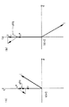
図2は図1に示すインバータ装置の制御時のベクトル図である。
図3は図2においてVdを0とした場合のベクトル図である。
図4は図1に示すインバータ装置の電流制限回路のブロック図である。
図1において、11aは加速度を修正する電流制限加速度補正手段、11a’は周波数指令と電流制限時出力周波数とを切替える周波数指令切替え手段、12aは電流の大きさI1と電流位相θiを出力する電流検出手段、13は検出電流I1と過電流制限値Imaxを比較する電流比較手段、14は比較結果を出力するリミット回路、15は電圧制限値ΔVを演算する電圧制限値演算手段、16は電圧制限ベクトルΔVq、ΔVdを求める電圧制限ベクトル演算手段、17a、bは電圧制限ベクトルの加算手段である。
なお、その他の図5と同一構成には同一符号を付し重複する説明は省略する
図4において、29a、29bは電流制限回路の無効手段であり、Icla’は第2の電流制限値、Iclb’、Ioc’は第3の電流制限値である。
なお、その他の図6と同一構成には同一符号を付し重複する説明は省略する。
【0009】
つぎに動作について説明する。
先ず、電流検出手段12aにより電流の大きさI1と、基準位相θに対する電流位相θiを求め、電流比較手段13によって設定した電流制限値Imaxから電流の大きさI1を減算し、リミット回路14によって減算結果が負の場合は0とし、電圧制限演算手段15でゲイン及びフィルタ処理(K/1+Ts)を施して電圧制限値ΔVを求める。電圧制限ベクトル演算手段16では、求めた電圧制限値ΔVと電流位相θiより次式で、
ΔVq=−ΔVsinθi
ΔVd=−ΔVcosθi
dq軸電圧制限値ΔVq、ΔVdを求める。
なお、電流検出値Id、Iqを用いて、
ΔVq=−ΔV×Iq/I1
ΔVd=−ΔV×Id/I1
として求めても同じ結果が得られる。
次に、演算したΔVq、ΔVdを電圧指令Vq* 、Vd* に加算手段17a、17bにより加算して出力電圧指令Vq、Vdを求めPWM指令演算部9により3相(UVW相)の電圧指令を求めてPWMパターンに変換し、ゲートドライバ回路10へ出力し電動機IMに電圧を印加する。これにより瞬時に電流を制限することが可能になる。
この間の電圧制限ベクトルΔV、電圧指令ベクトルV* 、電流ベクトルIの関係は、図2(a)に力行状態の場合を、図2(b)に回生状態の場合を示している。
図2(a)ではq軸上の電圧指令V*に対して電流と逆方向の電圧制限ベクトルΔVを加算し、印加電圧Vを小さくして、電流ベクトルIを制限する様子を示している。
図2(b)に示す回生状態では、逆に同方向にΔVを加算して印加電圧Vを大きくして電流ベクトルIを制限する様子を示している。
このように電動機の状態に関係なく瞬時に電流を制限することが可能になる。
【0010】
また、V/f制御によりモータ等を制御する場合、モータや負荷の状態によって不安定になる場合がある。このような状態の時、図2のようにdq軸それぞれに対して電圧補正を行うと、q軸方向は制御可能であるが、d軸方向は制御を行っていないため不安定状態を回避できなくなる場合がある。
従って、図3に示すように、ΔVdを0としてΔVqのみを電圧指令V* に加算するように制御することによって、これを回避できるようにしている。
図3(a)は力行状態を、図3(b)は回生状態を示し、図3(a)では電圧指令V*に逆方向の電圧制限ベクトルΔVqを加算し電圧Vを小さくして、電流Iを制限している。図3(b)の場合は、逆に電圧Vを大きくして電流Iを制限している。実際に、電流が大きくなる場合は、制御が正常で回転数がある程度あれば、q軸の方向に増加するため、電流の抑制能力はΔVqのみの補正で十分である。
以上の操作によって電流を瞬時に制限することが可能になるが、定常的に電流を制限して、電動機の効率を考慮する場合は周波数を修正する必要がある。これに対応するために、図1に示す電流制限加速度補正手段11aは、電流位相θiを用いて電動機の状態が力行か回生かを判断して加速度の修正方向を設定し、電圧制限値ΔVを用いて加速度の大きさを修正する。修正量は設定値又は、電圧制限値ΔVの負荷方向成分計算値などを用いて計算する。
また、電流制限加速度補正手段11aは、負荷の状態により回生の場合は最大値が最高周波数、力行の場合は最小値が0となるように電流制限時の周波数指令を出力し、周波数指令切替え手段11a’により、周波数指令と電流制限時出力周波数とを切替える。
【0011】
なお、力行/回生の判断はq軸電流のみを参照する方法、無効電力から演算する方法等各種あるがここでは割愛する。
回転方向と負荷方向により加速度補正を次のようにして行う。
a)正回転で力行の場合は正側に補正。
b)正回転で回生の場合は負側に補正。
c)逆回転で力行の場合は負側に補正。
d)逆回転で回生の場合は正側に補正。
加速度補正の最も単純な方法は、加速中であれば電圧制限値ΔVが0でない場合に力行負荷であれば加速を停止し、定常運転中であればΔVが0でない場合に力行中なら減速、回生中なら加速となるように加減速度設定値を加速度に代入する方法であるが、これらの方法でも十分に過電流を抑制できる。
また、予期せぬ電流変動があった場合のための保護対策として、図4に示す電流制限回路を用いる。図4の回路では、検出電流I1が電流制限値Imaxより大きい過電流レベルIoc’より大きい場合は、ゲート遮断回路27によりゲート遮断信号を選択・出力する。
電流I1がそれより小さい場合は、更に、電流制限レベルIclb’と比較して電流I1の方が大きければ、同様にゲート遮断信号を出力する。
電流I1がそれより小さく、電流制限レベルIcla’よりも大きい場合は、0電圧パターンを出力することになる。
この場合の各レベルの大小関係は次のようになっている。
Ioc’>Iclb’>Icla’>Imax
しかも、図1に示した電圧制限ベクトルΔVq、ΔVd及び電流制限加速度補正等の制御によって、かなりの部分で制限が可能となるため、各過電流レベルIoc’、Iclb’、Icla’は図6の従来例で示した対応する各過電流レベルIoc、Iclb、Iclaをアップした値(Ioc’>Ioc、Iclb’>Ic1b、Icla’>Icla)と設定することが可能になり、ストール防止が図られる。
また、用途によっては図1の制御で十分な場合もあるので、無効手段29a、29bにより図4の電流制限回路を切離し無効にして、O電圧切替え回路25とゲート遮断選択回路27の切替え部を除外することができる。
なお、この無効手段29は電流制限回路を所望の形態(自動/手動も含み)でON/OFFできれば如何なる方式でも構わない。
このように、本実施の形態によれば、電流の位相θiと電流の大きさI1を検出して、電流の大きさI1と電流制限値Imaxを比較して電圧制限値ΔVを求め、これを電流位相と逆方向になるように変換して電圧制限ベクトルΔVq、ΔVdを求め、電圧指令に加算して瞬時の電流制限を可能にすると共に、電圧制限値ΔVと電流位相θiを用いて加速度を修正することにより、ストールを防止して効率良く運転することが可能になる。
【0012】
【発明の効果】
以上説明したように、本発明によれば、電圧指令に対して電流制限値を超過した分に比例し電流ベクトルと逆方向あるいは逆方向の内の電圧指令軸上の成分の電圧制限ベクトルを加えることにより、瞬時に電流を制限することができるようになり、更に、3つのレベルの電流制限方法を持たせることによって、電流による素子の破壊と、ストールを確実に防止することができる。
また、電圧制限値と電流位相とから加速度を補正することによって定常的に電流を制限し、誘導電動機等を効率良く運転することができる。
【図面の簡単な説明】
【図1】本発明の実紙の形態に係るインバータ装置によるV/f制御の制御ブロック図である。
【図2】図1に示すインバータ装置の制御時のベクトル図である。
【図3】図2においてVdを0とした場合のベクトル図である。
【図4】図1に示すインバータ装置の電流制限回路のブロック図である。
【図5】従来のインバータ装置によるV/f制御の制御ブロック図である。
【図6】図5に示すインバータ装置の電流制限回路のブロック図である。
【図7】従来の周波数−電圧パターンを示す図である。
【図8】従来のインバータ装置の制御時のベクトル図である。
【符号の説明】
1 周波数指令演算部
2 加速指令演算手段
3 加速周波数積分手段
4 指令値制限手段
5 滑り周波数演算手段
6 出力周波数
7 V/f演算部
8 位相演算手段
9 PWM指令演算部
10 ゲートドライバ回路
11a 電流制限加速度補正手段
11a’ 周波数指令切替え手段
12a 電流検出手段
13 電流比較手段
14 リミット回路
15 電圧制限値演算手段
16 電圧制限ベクトル演算手段
17a q軸加算手段
17b d軸加算手段
18 0電圧パターン発生回路
19、20、21 比較器
22、23、24 ラッチ回路
25 0電圧切替え回路
26 オンディレイ回路
27 ゲート遮断選択回路
28 ゲート遮断選択回路
29 無効手段[0001]
BACKGROUND OF THE INVENTION
The present invention relates to an inverter device that enhances suppression of overcurrent when an induction motor or the like is driven by V / f control.
[0002]
[Prior art]
Conventionally, when V / f control of an induction motor is performed, if there is a sudden acceleration or a sudden change in load, the current increases. In that case, if a current exceeding the allowable amount flows to the semiconductor element of the inverter device, the element is destroyed, so an overcurrent level is set. I try to deter destruction.
In addition, since the gate cut-off by the overcurrent protection function needs to be restarted, a gate cut-off circuit with a function of automatically returning at a level lower than the previous overcurrent level and a 0 voltage pattern output to a lower level The current limiting circuit is used to limit the current and protect the semiconductor.
In addition, the magnitude of the current can be corrected by detecting the magnitude of the current, or by stopping the acceleration if the current increases during acceleration and decreasing the frequency if the current increases during steady operation. Control focused only on it.
[0003]
Next, the actual V / f control will be described with a specific example.
FIG. 5 is a control block diagram of conventional V / f control. FIG. 8 shows an example of the voltage command Vq * and current I and the voltage component of the motor in a certain power running state of the V / f control as shown in FIG. 5, where the d axis is the reference phase of the control output. 2 shows a control mode for controlling the q-axis voltage set at a position of 90 degrees from the d-axis.
In the V / f control shown in FIG. 5, θ represents the position of the d axis viewed from a certain reference position (for example, U phase). The frequency
Further, at the time of deceleration, when the lower limit value of the speed integrated by the acceleration frequency integrating means 3 becomes the frequency command value by the command value limiting means 4, the deceleration is stopped. The slip frequency means 5 calculates the slip frequency of the motor from the detected torque current value to obtain the
The V / f calculation unit 7 obtains a voltage command Vq * from the output frequency from a frequency-voltage pattern as shown in FIG. Further, the output phase θ is obtained by integration by the phase calculating means 8 from the output frequency, and the three-phase (UVW phase) voltage command is obtained by the PWM command calculating unit 9 from the voltage commands Vq *, Vd * (value 0) and θ. The PWM pattern is converted and output to the
Conventionally, as a measure for preventing a stall (stop state), the current detection means 12b detects the current magnitude I1, and when the acceleration correction means 11b increases the magnitude of I1, the acceleration is delayed if acceleration is in progress. During steady operation, the vehicle was accelerated (decelerated) with a negative value. However, if there is a sudden acceleration or a sudden load change, the increase in current cannot be suppressed and a stall may occur due to hard overcurrent protection.
[0004]
To solve this problem, a measure is taken to prevent a stall while creating a current limiting circuit as shown in FIG. 6 and suppressing the current.
As shown in FIG. 6, the voltage conversion means 9a in the PWM command calculation unit 9 converts the voltage from the dq axis to the UVW phase voltage, performs PWM modulation by the
Ioc>Iclb> Icla
First, the current detection value I1 and the overcurrent level Ioc are compared by the
When the current is smaller than that, the result of comparing the current detection value I1 and the next current limit level Iclb by the
If the current is smaller, the current detection value I1 is compared with the next current limit level Icl by the
The
Next, as a method other than the correction based on the magnitude of the current, the voltage is corrected using a voltage limit vector in the direction opposite to the detected current, and PI control is performed on the magnitude of the voltage limit vector to perform a speed command. There is a method for performing the correction.
[0005]
[Problems to be solved by the invention]
However, in the case of the method of FIG. 6, since the current is limited by correcting the magnitude of the voltage from the magnitude of the current, if the voltage is reduced when the motor is in the regenerative state, the current is increased. As described above, the current cannot be limited depending on the state of the electric motor, and conversely, the current becomes large and the overcurrent protection function works to cause a stall due to the gate interruption.
Further, in the method using zero voltage, the current is distorted and power is not supplied to the electric motor, resulting in poor efficiency. For this reason, there has been a problem that the demand has not been satisfied even though a current limiting method with high power efficiency is desired while reliably dropping the current.
Furthermore, when correcting the voltage using the voltage limit vector in the opposite direction to the detected current, and correcting the speed command by applying PI control to the voltage limit vector, the voltage is compensated with the vector in the direction opposite to the current. It is possible to reduce the current, but in order to perform PI control focusing only on the magnitude of the current with respect to the speed command, the correction works when the motor is in a power running state, but in the case of regeneration In some cases, the frequency correction may adversely affect the current. Further, since the speed correction method is PI control, when a large load is applied instantaneously, a large frequency correction corresponding to the load is applied, so that the speed tends to become unstable. In addition, the integral accumulates in the unstable state and there is a risk of runaway. In addition, the correction of voltage DVq and DVd is performed not only in the direction of the voltage control axis but also in the direction orthogonal thereto, so that it is difficult to suppress the occurrence of problems such as turbulence and stability cannot be secured. there were. Therefore, an object of the present invention is to provide an inverter device capable of operating the motor efficiently and stably by reliably limiting the current regardless of the state of the motor to prevent element destruction and stalling, and current limitation thereof. It is to provide a method.
[0006]
[Means for Solving the Problems]
In order to achieve the above object, the invention of the inverter device according to
According to a second aspect of the present invention, in the inverter device according to the first aspect, when the voltage limit value calculation means filters the value proportional to the excess when the current limit value is exceeded, the first limit delay filter is used. The result is output as a voltage limit value.
According to a third aspect of the present invention, in the inverter device according to the first or second aspect, the voltage limit vector computing means converts the voltage limit value into a vector in a direction opposite to the current phase. Yes.
According to a fourth aspect of the present invention, in the inverter device according to the third aspect, the voltage limit vector computing means orthogonally intersects the voltage command vector direction with respect to the voltage limit value in a vector in a direction opposite to the current phase. The voltage limiting vector component to be output is output as 0.
According to a fifth aspect of the invention, in the inverter device according to the first or second aspect, the zero voltage is forcibly applied while the magnitude of the current exceeds a second current limit value larger than the current limit value. Second current limiting means for outputting the PWM pattern, and third current limiting means for interrupting the gate while the magnitude of the current exceeds a third current limit value larger than the second current limit value. It is characterized by having.
According to a sixth aspect of the invention, there is provided the inverter device according to the fifth aspect, further comprising means for invalidating the function with respect to the second current limiting means and the third current limiting means. Yes.
The invention of the current limiting method for an inverter device according to claim 7 is to obtain a voltage command vector from a frequency command value and a voltage command value obtained from the frequency command value by V / f calculation, and In the current limiting method of the inverter device that performs a protection operation when an overcurrent is detected based on PWM modulation based on the PWM modulation, the output current of the inverter device is detected and the magnitude of the current is calculated from the output current A current vector composed of I1 and a current phase θi is obtained , and when the magnitude of the current exceeds a current limit value Imax, a voltage limit value ΔV proportional to the excess is obtained, and the voltage limit value ΔV is based on the current phase θi. voltage limitation Te vector? Vq, limit the current to instantaneously perform the voltage correction by adding the voltage command vector into a .DELTA.Vd, acceleration corrected based on the current phase Seeking direction, obtains the acceleration correction amount based on the voltage limit value, it is characterized by performing a good current limiting of the power efficiency by modifying the acceleration command of the frequency by the acceleration correction amount and the acceleration correction direction.
In the current limiting method of the inverter device according to claim 7, the voltage limiting value ΔV is proportional to the excess when the magnitude of the current exceeds the current limiting value Imax. The value is filtered by a first-order lag filter to remove harmonics and output.
In addition, according to a ninth aspect of the present invention, in the current limiting method for an inverter device according to the seventh or eighth aspect, the voltage limiting vectors ΔVq and ΔVd have the voltage limiting value ΔV as a vector in a direction opposite to the current phase θi. It is characterized in that it is created by conversion into ΔVq = −ΔVsinθi (or ΔVq = −ΔV × Iq / I1) and ΔVd = −ΔVcosθi (or Δd = −ΔV × Id / I1).
In the current limiting method for an inverter device according to claim 9, the voltage limiting vector may be configured such that the voltage limiting value ΔV is a vector Δ Vq or Δ Vd in a direction opposite to the current phase θi. The voltage limit vector component ΔVd orthogonal to the voltage command vector direction is output at 0.
According to an eleventh aspect of the present invention, in the current limiting method of the inverter device according to the seventh or eighth aspect, the magnitude of the current exceeds a second current limit value Icl ′ that is larger than the current limit value Imax. A zero voltage PWM pattern is forcibly output during the interval, and the gate is maintained while the current exceeds the third current limit values Iclb ′ and Ioc ′ larger than the second current limit value Icl ′. It is characterized in that the protection operation is performed by blocking.
According to a twelfth aspect of the present invention, in the current limiting method for an inverter device according to the eleventh aspect, the protection function by the second and third current limit values can be invalidated. Yes.
[0007]
According to this inverter device and its overcurrent suppression method, a voltage limit value ΔV proportional to the excess exceeding the overcurrent limit value Imax in FIG. 1 is obtained, and the voltage limit value ΔVq based on the current phase is obtained as the voltage limit value. By converting to ΔVd and adding it to the voltage command vector, instantaneous overcurrent can be suppressed, and the current is limited by correcting the frequency acceleration command based on the voltage limit value ΔV and the current phase θi. While avoiding stalls, it is possible to drive efficiently.
At that time, since the voltage limit vector is obtained after passing through the first-order lag filter (K / 1 + Ts) for the voltage limit value ΔV, it is possible to perform stable compensation by removing harmonic components contained in the current. Yes.
In addition, when the voltage limit value ΔV is converted into the voltage limit vectors ΔVq and ΔVd, the voltage limit vector is obtained so as to be in the opposite direction to the current direction, and compensation is performed. It becomes possible to limit the current. Also, when controlling a motor or the like, a voltage command vector that is V / f controlled by setting a direction component ΔVd orthogonal to the voltage command vector among components in the direction opposite to the current of the voltage limit vector to 0. By performing compensation only in the direction of, stable current limit control becomes possible.
As a protective measure in the case where the current limit as described above does not work normally, the current limit I1 is forced while the current magnitude I1 exceeds the second overcurrent limit value Icl ′ larger than the overcurrent limit value Imax. When a protection operation is performed by outputting a zero voltage PWM pattern, and while the magnitude of the current exceeds the third overcurrent limit value Iclb ′ or Ioc ′ larger than the second overcurrent limit value Icl ′, Since the gate is cut off for protection, even if the current magnitude I1 greatly exceeds the overcurrent limit value Imax, the second and third overcurrent limit values 1c1a ′, Iclb ′, and Ioc ′ Since three levels of protection are performed, reliable and safe overcurrent suppression is possible. In this case, the magnitude relationship between the setting levels is Ioc ′> Iclb ′>Icla> Imax.
Therefore, in the case of the present invention, since it can be almost suppressed by suppression by the overcurrent limit value Imax, the values of the setting levels Ioc, Iclb, Icl of the CLA and CLB circuits in which the overcurrent level in the conventional case is set are increased. be able to.
Further, since the control of the overcurrent limit value Imax is almost sufficient, switching means 29a and 29b for disabling the CLA and CLB circuits are provided so that the CLA and CLB circuits can be turned on / off to enable a wide range of control. .
[0008]
DETAILED DESCRIPTION OF THE INVENTION
Hereinafter, embodiments of the present invention will be described with reference to the drawings.
FIG. 1 is a control block diagram of V / f control by the inverter apparatus according to the embodiment of the present invention.
FIG. 2 is a vector diagram when controlling the inverter device shown in FIG.
FIG. 3 is a vector diagram when Vd is 0 in FIG.
FIG. 4 is a block diagram of a current limiting circuit of the inverter device shown in FIG.
In FIG. 1, 11a is a current limiting acceleration correcting means for correcting acceleration, 11a 'is a frequency command switching means for switching between a frequency command and a current limiting output frequency, and 12a is a current that outputs a current magnitude I1 and a current phase θi. Detection means, 13 is a current comparison means for comparing the detected current I1 and the overcurrent limit value Imax, 14 is a limit circuit for outputting the comparison result, 15 is a voltage limit value calculation means for calculating the voltage limit value ΔV, and 16 is a voltage limit Voltage limit vector calculation means for obtaining vectors ΔVq and ΔVd, and 17a and b are voltage limit vector addition means.
In FIG. 4, the same components as those in FIG. 5 are assigned the same reference numerals and redundant description is omitted. In FIG. 4, 29 a and 29 b are invalid means of the current limiting circuit, Icl ′ is the second current limiting value, Iclb ', Ioc' is the third current limit value.
In addition, the same code | symbol is attached | subjected to the other same structure as FIG. 6, and the overlapping description is abbreviate | omitted.
[0009]
Next, the operation will be described.
First, the current magnitude I1 and the current phase θi with respect to the reference phase θ are obtained by the current detection means 12a, the current magnitude I1 is subtracted from the current limit value Imax set by the current comparison means 13, and the
ΔVq = −ΔVsin θi
ΔVd = −ΔVcos θi
The dq axis voltage limit values ΔVq and ΔVd are obtained.
In addition, using the current detection values Id and Iq,
ΔVq = −ΔV × Iq / I1
ΔVd = −ΔV × Id / I1
The same result can be obtained even if
Then, the calculated? Vq, voltage command Vq * to .DELTA.Vd, Vd * to the
The relationship between the voltage limit vector ΔV, the voltage command vector V * , and the current vector I during this period is shown in FIG. 2A for the power running state and FIG. 2B for the regenerative state.
FIG. 2A shows a state in which the voltage vector V in the direction opposite to the current is added to the voltage command V * on the q axis, the applied voltage V is reduced, and the current vector I is limited.
In the regenerative state shown in FIG. 2B, on the contrary, ΔV is added in the same direction to increase the applied voltage V to limit the current vector I.
In this way, the current can be instantaneously limited regardless of the state of the electric motor.
[0010]
Moreover, when controlling a motor etc. by V / f control, it may become unstable by the state of a motor or load. In such a state, if voltage correction is performed for each of the dq axes as shown in FIG. 2, the q-axis direction can be controlled, but an unstable state can be avoided because the d-axis direction is not controlled. It may disappear.
Therefore, as shown in FIG. 3, this can be avoided by controlling ΔVd to be 0 and adding only ΔVq to the voltage command V * .
3A shows a power running state, FIG. 3B shows a regenerative state, and in FIG. 3A, a voltage limit vector ΔVq in the reverse direction is added to the voltage command V * to reduce the voltage V to reduce the current. I is limited. In the case of FIG. 3B, the voltage V is increased to limit the current I. In fact, when the current increases, if the control is normal and the rotation speed is some, the current increases in the q-axis direction. Therefore, it is sufficient to correct the current only by correcting ΔVq.
Although the current can be instantaneously limited by the above operation, the frequency needs to be corrected when the current is constantly limited and the efficiency of the motor is taken into consideration. In order to cope with this, the current limit acceleration correction means 11a shown in FIG. 1 determines whether the state of the motor is power running or regenerative using the current phase θi, sets the acceleration correction direction, and sets the voltage limit value ΔV. Use to correct the magnitude of acceleration. The correction amount is calculated using a set value or a load direction component calculated value of the voltage limit value ΔV.
Further, the current limit acceleration correction means 11a outputs a frequency command at the time of current limit so that the maximum value is the maximum frequency in the case of regeneration and the minimum value is 0 in the case of powering depending on the load state, and the frequency command switching means The frequency command and the current limiting output frequency are switched by 11a ′.
[0011]
Note that there are various methods such as a method of referring to only the q-axis current and a method of calculating from the reactive power for the determination of power running / regeneration, but these are omitted here.
Acceleration correction is performed as follows according to the rotation direction and load direction.
a) In the case of power running with forward rotation, correct to the positive side.
b) When regenerating in positive rotation, correct to negative side.
c) In the case of power running with reverse rotation, correct to the negative side.
d) When regenerating with reverse rotation, correct to the positive side.
The simplest method of acceleration correction is to stop acceleration if the power limit load is not 0 when the voltage limit value ΔV is 0, and to decelerate if power is running when ΔV is not 0 during steady operation, In this method, the acceleration / deceleration set value is substituted for acceleration so that acceleration is achieved during regeneration, but these methods can also sufficiently suppress overcurrent.
Further, a current limiting circuit shown in FIG. 4 is used as a protective measure when there is an unexpected current fluctuation. In the circuit of FIG. 4, when the detected current I1 is larger than the overcurrent level Ioc ′ larger than the current limit value Imax, the
When the current I1 is smaller than that, if the current I1 is larger than the current limit level Iclb ′, the gate cutoff signal is similarly output.
When the current I1 is smaller than that and larger than the current limit level Icl ′, a zero voltage pattern is output.
In this case, the level relationship between the levels is as follows.
Ioc ′> Iclb ′>Icla> Imax
In addition, since control is possible in a considerable part by the control such as the voltage limit vectors ΔVq and ΔVd and the current limit acceleration correction shown in FIG. 1, the overcurrent levels Ioc ′, Iclb ′, and Icl ′ are shown in FIG. The corresponding overcurrent levels Ioc, Iclb, and Icl shown in the conventional example can be set to values (Ioc ′> Ioc, Iclb ′> Ic1b, Icl ′> Icl), and stall prevention can be achieved. .
Further, depending on the application, the control of FIG. 1 may be sufficient, so that the current limiting circuit of FIG. 4 is disconnected and disabled by the invalidating means 29a and 29b, and the switching unit of the O
The invalidating means 29 may be of any type as long as the current limiting circuit can be turned on / off in a desired form (including automatic / manual).
As described above, according to the present embodiment, the current phase θi and the current magnitude I1 are detected, the current magnitude I1 and the current limit value Imax are compared, and the voltage limit value ΔV is obtained. The voltage limit vectors ΔVq and ΔVd are obtained by conversion so as to be in the opposite direction to the current phase, and added to the voltage command to enable instantaneous current limit, and the acceleration is calculated using the voltage limit value ΔV and the current phase θi. By correcting, it becomes possible to prevent stall and to operate efficiently.
[0012]
【The invention's effect】
As described above, according to the present invention, the voltage limit vector of the component on the voltage command axis in the reverse direction or the reverse direction of the current vector is added in proportion to the amount exceeding the current limit value with respect to the voltage command. As a result, the current can be instantaneously limited, and further, by providing a current limiting method of three levels, it is possible to reliably prevent the destruction of the element and the stall due to the current.
In addition, by correcting the acceleration from the voltage limit value and the current phase, the current is constantly limited, and the induction motor or the like can be operated efficiently.
[Brief description of the drawings]
FIG. 1 is a control block diagram of V / f control by an inverter device according to a form of real paper of the present invention.
FIG. 2 is a vector diagram when controlling the inverter device shown in FIG. 1;
FIG. 3 is a vector diagram when Vd is 0 in FIG. 2;
4 is a block diagram of a current limiting circuit of the inverter device shown in FIG. 1; FIG.
FIG. 5 is a control block diagram of V / f control by a conventional inverter device.
6 is a block diagram of a current limiting circuit of the inverter device shown in FIG. 5. FIG.
FIG. 7 is a diagram showing a conventional frequency-voltage pattern.
FIG. 8 is a vector diagram during control of a conventional inverter device.
[Explanation of symbols]
DESCRIPTION OF
Claims (12)
前記インバータ装置の出力電流を検出して前記出力電流から電流の大きさと電流位相とからなる電流ベクトルを求める電流検出手段と、前記電流の大きさが電流制限値を超えた時に超過分に比例した電圧制限値を求める電圧制限値演算手段と、前記電圧制限値を前記電流位相に基づいて電圧制限ベクトルに変換する電圧制限ベクトル演算手段と、前記電圧指令ベクトルに前記電圧制限ベクトルを加算する電圧補正手段と、前記電流位相に基づいて加速度修正方向を求め、前記電圧制限値に基づいて加速度修正量を求め、前記加速度修正方向と前記加速度修正量により周波数の加速度指令を修正する加速度修正手段とを備えたことを特徴とするインバータ装置。In an inverter device for obtaining a voltage command vector from a frequency command value and a voltage command value obtained by V / f calculation from the frequency command value, and performing PWM modulation based on the voltage command vector to output a voltage,
Current detection means for detecting an output current of the inverter device to obtain a current vector comprising a current magnitude and a current phase from the output current; and when the current magnitude exceeds a current limit value, the current detection means is proportional to the excess Voltage limit value calculating means for obtaining a voltage limit value, voltage limit vector calculating means for converting the voltage limit value into a voltage limit vector based on the current phase, and voltage correction for adding the voltage limit vector to the voltage command vector And an acceleration correction means for determining an acceleration correction direction based on the current phase , determining an acceleration correction amount based on the voltage limit value, and correcting an acceleration command of a frequency based on the acceleration correction direction and the acceleration correction amount. An inverter device comprising:
前記インバータ装置の出力電流を検出して前記出力電流から電流の大きさI1と電流位相θiからなる電流ベクトルを求め、前記電流の大きさが電流制限値Imaxを超えた時に超過分に比例した電圧制限値ΔVを求め、前記電圧制限値ΔVを前記電流位相θiに基づいて電圧制限ベクトルΔVq、ΔVdに変換し前記電圧指令ベクトルに加算して電圧補正を行い瞬時に電流を制限し、前記電流位相に基づいて加速度修正方向を求め、前記電圧制限値に基づいて加速度修正量を求め、前記加速度修正方向と前記加速度修正量により周波数の加速度指令を修正してパワー効率の良い電流制限を行うことを特徴とするインバータ装置の電流制限方法。When a voltage command vector is obtained from a frequency command value and a voltage command value obtained by V / f calculation from the frequency command value, a voltage is output by PWM modulation based on the voltage command vector, and an overcurrent is detected In the current limiting method of the inverter device that performs the protective operation,
A voltage proportional to the excess when the magnitude of the current exceeds the current limit value Imax is obtained by detecting the output current of the inverter device, obtaining a current vector composed of the current magnitude I1 and the current phase θi from the output current . A limit value ΔV is obtained, the voltage limit value ΔV is converted into voltage limit vectors ΔVq and ΔVd based on the current phase θi, added to the voltage command vector, voltage correction is performed to instantaneously limit the current, and the current phase It obtains an acceleration correction direction based on, obtains an acceleration correction amount based on the voltage limit value, to make a good current limiting of the power efficiency by modifying the acceleration command of the frequency by the acceleration correction amount and the acceleration correction direction A current limiting method for an inverter device.
Priority Applications (7)
| Application Number | Priority Date | Filing Date | Title |
|---|---|---|---|
| JP2000211426A JP4131079B2 (en) | 2000-07-12 | 2000-07-12 | Inverter device and current limiting method thereof |
| EP20010947964 EP1306967B1 (en) | 2000-07-12 | 2001-07-10 | Inverter device and current limiting method therefor |
| PCT/JP2001/005986 WO2002005415A1 (en) | 2000-07-12 | 2001-07-10 | Inverter device and current limiting method therefor |
| CNB018126472A CN1227805C (en) | 2000-07-12 | 2001-07-10 | Inverter device and current limiting method therefor |
| KR1020037000031A KR100798511B1 (en) | 2000-07-12 | 2001-07-10 | Inverter device and current limiting method therefor |
| US10/332,509 US6804130B2 (en) | 2000-07-12 | 2001-07-10 | Inverter device and current limiting method therefor |
| TW090116895A TWI243532B (en) | 2000-07-12 | 2001-07-10 | Inverter device and current limiting method therefor |
Applications Claiming Priority (1)
| Application Number | Priority Date | Filing Date | Title |
|---|---|---|---|
| JP2000211426A JP4131079B2 (en) | 2000-07-12 | 2000-07-12 | Inverter device and current limiting method thereof |
Publications (2)
| Publication Number | Publication Date |
|---|---|
| JP2002034289A JP2002034289A (en) | 2002-01-31 |
| JP4131079B2 true JP4131079B2 (en) | 2008-08-13 |
Family
ID=18707535
Family Applications (1)
| Application Number | Title | Priority Date | Filing Date |
|---|---|---|---|
| JP2000211426A Expired - Fee Related JP4131079B2 (en) | 2000-07-12 | 2000-07-12 | Inverter device and current limiting method thereof |
Country Status (7)
| Country | Link |
|---|---|
| US (1) | US6804130B2 (en) |
| EP (1) | EP1306967B1 (en) |
| JP (1) | JP4131079B2 (en) |
| KR (1) | KR100798511B1 (en) |
| CN (1) | CN1227805C (en) |
| TW (1) | TWI243532B (en) |
| WO (1) | WO2002005415A1 (en) |
Families Citing this family (38)
| Publication number | Priority date | Publication date | Assignee | Title |
|---|---|---|---|---|
| JP2002238293A (en) * | 2001-02-14 | 2002-08-23 | Mitsubishi Electric Corp | Motor control apparatus |
| KR101034129B1 (en) | 2004-11-11 | 2011-05-13 | 엘지전자 주식회사 | Over current limit apparatus and method for inverter system |
| FR2881296B1 (en) * | 2005-01-27 | 2007-03-09 | Schneider Toshiba Inverter | METHOD AND SYSTEM FOR LIMITING THE CURRENT OUTPUT OF A SPEED DRIVE OPERATING ACCORDING TO A U / F CONTROL ACT |
| JP4746107B2 (en) * | 2005-11-21 | 2011-08-10 | アーベーベー・シュバイツ・アーゲー | Method for operating a converter circuit and apparatus for performing the method |
| KR101149125B1 (en) * | 2005-12-19 | 2012-05-25 | 두산산업차량 주식회사 | Apparatus of controlling the motor for driving an electric forklift truck |
| KR20070072088A (en) * | 2005-12-30 | 2007-07-04 | 엘지전자 주식회사 | Apparatus and method for conrolling inverter |
| KR100761268B1 (en) * | 2006-01-06 | 2007-09-28 | 엘지전자 주식회사 | Driving control apparatus and method for reciprocating compressor |
| US7193388B1 (en) | 2006-02-02 | 2007-03-20 | Emerson Electric Co. | Offset PWM signals for multiphase motor |
| KR100734530B1 (en) * | 2006-04-12 | 2007-07-04 | 주식회사 피플웍스 | Limited current circuit for lcd backlight inverter |
| JP5131725B2 (en) * | 2006-10-23 | 2013-01-30 | 国立大学法人長岡技術科学大学 | Control device for power converter |
| JP2008167630A (en) * | 2007-01-05 | 2008-07-17 | Fuji Electric Fa Components & Systems Co Ltd | Control unit for electric power converter |
| CN101453191B (en) * | 2007-12-07 | 2010-07-14 | 上海智维电子科技有限公司 | Ultra-start-up control driving power for digital controlled air weaving machine |
| JP5251104B2 (en) * | 2007-12-11 | 2013-07-31 | 富士電機株式会社 | Inverter device |
| US7843162B2 (en) * | 2008-03-13 | 2010-11-30 | Gm Global Technology Operations, Inc. | Current regulator and current control method and system for AC motors |
| JP2011176918A (en) * | 2010-02-23 | 2011-09-08 | On Semiconductor Trading Ltd | Motor driver circuit |
| WO2011108169A1 (en) * | 2010-03-03 | 2011-09-09 | 株式会社安川電機 | Inverter device and control method thereof |
| IT1402368B1 (en) * | 2010-04-15 | 2013-09-04 | Ansaldo Electric Drives S P A Ora Ansaldo En Holding S P A | ELECTRIC MACHINE, CONTROL DEVICE FOR CHECKING ITS ELECTRIC MACHINE, ELECTRIC PROPULSION SYSTEM INCLUDING THE ELECTRIC MACHINE AND THE DEVICE FOR CONTROL AND THE METHOD OF CHECKING THAT ELECTRIC MACHINE |
| US9287812B2 (en) * | 2013-06-29 | 2016-03-15 | Rockwell Automation Technologies, Inc. | Method and apparatus for stability control of open loop motor drive operation |
| US9490738B2 (en) | 2013-01-16 | 2016-11-08 | Rockwell Automation Technologies, Inc. | Sensorless motor drive vector control |
| US10158314B2 (en) | 2013-01-16 | 2018-12-18 | Rockwell Automation Technologies, Inc. | Feedforward control of motor drives with output sinewave filter |
| JP5811363B2 (en) * | 2013-03-13 | 2015-11-11 | 株式会社デンソー | Rotating electrical machine control device and electric power steering device using the same |
| JP5835272B2 (en) * | 2013-05-30 | 2015-12-24 | トヨタ自動車株式会社 | Control device for vehicle power unit |
| DE102014103027A1 (en) * | 2014-03-07 | 2015-09-10 | Baumüller Nürnberg GmbH | Tracking controller for a V / f-controlled asynchronous machine |
| KR101601444B1 (en) | 2014-07-04 | 2016-03-21 | 현대자동차주식회사 | Device and method for controlling inverter of motor driving system |
| US9654035B1 (en) * | 2014-09-30 | 2017-05-16 | Sandia Corporation | High-temperature brushless DC motor controller |
| CN104868799B (en) * | 2014-12-08 | 2017-08-04 | 北京车和家信息技术有限责任公司 | A kind of acquisition motor rotor position, the method and device of speed |
| US9716460B2 (en) | 2015-01-28 | 2017-07-25 | Rockwell Automation Technologies, Inc. | Method and apparatus for speed reversal control of motor drive |
| US9774284B2 (en) | 2015-02-19 | 2017-09-26 | Rockwell Automation Technologies, Inc. | Rotor position estimation apparatus and methods |
| US9595896B1 (en) | 2015-12-16 | 2017-03-14 | Rockwell Automation Technologies, Inc. | Methods and systems for sensorless closed loop motor speed and torque control |
| US9800190B2 (en) | 2016-02-03 | 2017-10-24 | Rockwell Automation Technologies, Inc. | Control of motor drives with output sinewave filter capacitor current compensation using sinewave filter transfer function |
| EP3437182A4 (en) * | 2016-03-30 | 2019-08-07 | Ideal Power Inc. | Microgrid power architecture |
| US9985565B2 (en) | 2016-04-18 | 2018-05-29 | Rockwell Automation Technologies, Inc. | Sensorless motor drive vector control with feedback compensation for filter capacitor current |
| US10020766B2 (en) | 2016-11-15 | 2018-07-10 | Rockwell Automation Technologies, Inc. | Current control of motor drives with output sinewave filter |
| JP2019080419A (en) | 2017-10-24 | 2019-05-23 | 株式会社日立産機システム | Power conversion device and control method thereof |
| JP6676830B1 (en) * | 2018-11-21 | 2020-04-08 | 東芝三菱電機産業システム株式会社 | Power converter |
| WO2021117459A1 (en) * | 2019-12-13 | 2021-06-17 | 株式会社安川電機 | Power conversion device, conveyance system, power conversion method, program, and diagnostic device |
| JP2021136730A (en) * | 2020-02-25 | 2021-09-13 | 株式会社Flosfia | Power conversion device and power conversion system |
| CN112398400A (en) * | 2020-09-12 | 2021-02-23 | 上海新时达电气股份有限公司 | Current limiting method and device for three-phase motor |
Family Cites Families (6)
| Publication number | Priority date | Publication date | Assignee | Title |
|---|---|---|---|---|
| JP2743382B2 (en) | 1988-05-27 | 1998-04-22 | 三菱電機株式会社 | Inverter device for driving induction motor |
| US4994950A (en) * | 1990-07-31 | 1991-02-19 | Eaton Corporation | Waveform generator for inverter control |
| JP3299417B2 (en) | 1995-07-28 | 2002-07-08 | 松下電工株式会社 | Inverter device |
| KR100237306B1 (en) * | 1997-03-25 | 2000-01-15 | 윤종용 | Vibration control method and device of 2nd order system |
| JP3684793B2 (en) * | 1997-11-17 | 2005-08-17 | 株式会社明電舎 | Inverter device |
| KR100651222B1 (en) * | 1999-08-12 | 2006-11-29 | 가부시키가이샤 야스카와덴키 | Method for controlling neutral point potential of inverter of neutral point clamping type |
-
2000
- 2000-07-12 JP JP2000211426A patent/JP4131079B2/en not_active Expired - Fee Related
-
2001
- 2001-07-10 EP EP20010947964 patent/EP1306967B1/en not_active Expired - Lifetime
- 2001-07-10 WO PCT/JP2001/005986 patent/WO2002005415A1/en active Application Filing
- 2001-07-10 TW TW090116895A patent/TWI243532B/en not_active IP Right Cessation
- 2001-07-10 CN CNB018126472A patent/CN1227805C/en not_active Expired - Fee Related
- 2001-07-10 KR KR1020037000031A patent/KR100798511B1/en not_active IP Right Cessation
- 2001-07-10 US US10/332,509 patent/US6804130B2/en not_active Expired - Lifetime
Also Published As
| Publication number | Publication date |
|---|---|
| KR20030027933A (en) | 2003-04-07 |
| CN1227805C (en) | 2005-11-16 |
| WO2002005415A1 (en) | 2002-01-17 |
| EP1306967B1 (en) | 2015-04-22 |
| CN1441994A (en) | 2003-09-10 |
| EP1306967A1 (en) | 2003-05-02 |
| EP1306967A4 (en) | 2014-03-12 |
| TWI243532B (en) | 2005-11-11 |
| KR100798511B1 (en) | 2008-01-28 |
| US6804130B2 (en) | 2004-10-12 |
| JP2002034289A (en) | 2002-01-31 |
| US20040052097A1 (en) | 2004-03-18 |
Similar Documents
| Publication | Publication Date | Title |
|---|---|---|
| JP4131079B2 (en) | Inverter device and current limiting method thereof | |
| JP4737087B2 (en) | Control device for permanent magnet synchronous motor | |
| JP6226566B2 (en) | Motor control device and construction machine having the same | |
| JP3684793B2 (en) | Inverter device | |
| JP4300831B2 (en) | Braking method and inverter apparatus for inverter-driven induction motor | |
| US20230327592A1 (en) | Electric motor control method and electric motor system | |
| JPH10313592A (en) | Motor control device and motor control method | |
| JP5392532B2 (en) | Induction motor control device | |
| CA2714698C (en) | Method and system for braking an ac motor | |
| JP2861418B2 (en) | Torque limiting method and control method for induction motor | |
| CN111418144B (en) | Motor control method and motor control device | |
| JP2013123288A (en) | Controller of motor | |
| CN111971892A (en) | Motor drive device, controller, and electric vehicle system | |
| KR102485408B1 (en) | Method for controlling inverter | |
| JPWO2019106729A1 (en) | Electric motor control method and electric motor control device | |
| JP2008167630A (en) | Control unit for electric power converter | |
| JP2008109719A (en) | Controller of power converter | |
| JP4771035B2 (en) | Control device for permanent magnet synchronous machine | |
| JP4488415B2 (en) | Power converter | |
| JP3462347B2 (en) | Control device for variable speed generator motor | |
| JP4774796B2 (en) | Permanent magnet synchronous motor drive device | |
| JP4051601B2 (en) | Variable speed control device for electric motor | |
| JP2004104959A (en) | Regenerative control method of power converter for driving motor | |
| JP2023072565A (en) | Motor control method and motor control device | |
| JP7424109B2 (en) | Power conversion device and its control method |
Legal Events
| Date | Code | Title | Description |
|---|---|---|---|
| A621 | Written request for application examination |
Free format text: JAPANESE INTERMEDIATE CODE: A621 Effective date: 20050831 |
|
| RD04 | Notification of resignation of power of attorney |
Free format text: JAPANESE INTERMEDIATE CODE: A7424 Effective date: 20060324 |
|
| RD04 | Notification of resignation of power of attorney |
Free format text: JAPANESE INTERMEDIATE CODE: A7424 Effective date: 20071129 |
|
| A131 | Notification of reasons for refusal |
Free format text: JAPANESE INTERMEDIATE CODE: A131 Effective date: 20080213 |
|
| A521 | Request for written amendment filed |
Free format text: JAPANESE INTERMEDIATE CODE: A523 Effective date: 20080404 |
|
| TRDD | Decision of grant or rejection written | ||
| A01 | Written decision to grant a patent or to grant a registration (utility model) |
Free format text: JAPANESE INTERMEDIATE CODE: A01 Effective date: 20080430 |
|
| A01 | Written decision to grant a patent or to grant a registration (utility model) |
Free format text: JAPANESE INTERMEDIATE CODE: A01 |
|
| A61 | First payment of annual fees (during grant procedure) |
Free format text: JAPANESE INTERMEDIATE CODE: A61 Effective date: 20080513 |
|
| FPAY | Renewal fee payment (event date is renewal date of database) |
Free format text: PAYMENT UNTIL: 20110606 Year of fee payment: 3 |
|
| R150 | Certificate of patent or registration of utility model |
Free format text: JAPANESE INTERMEDIATE CODE: R150 |
|
| FPAY | Renewal fee payment (event date is renewal date of database) |
Free format text: PAYMENT UNTIL: 20120606 Year of fee payment: 4 |
|
| FPAY | Renewal fee payment (event date is renewal date of database) |
Free format text: PAYMENT UNTIL: 20130606 Year of fee payment: 5 |
|
| FPAY | Renewal fee payment (event date is renewal date of database) |
Free format text: PAYMENT UNTIL: 20140606 Year of fee payment: 6 |
|
| LAPS | Cancellation because of no payment of annual fees |