Technical Field
The present invention relates to an image sensor for
ultrahigh-speed image capturing suitable for continuous image
capturing of high-speed motions such as breakage and explosion
of materials and high-speed flows.
Background Art
The speed of image capturing by normal solid-state image
sensors is limited by the information transfer capability of
a read-out line for reading out image information from the image
sensor to the outside of the image sensor. Precisely, the image
capturing speed is limited by the information processing
capabilities of an output circuit that performs processing
preceding the image information read-out and an AD converter
that performs processing succeeding the image information
read-out, that is, a sampling rate. A standard maximum sampling
rate of currently used image sensors is approximately 25 MHz
(25,000,000 pixels per second) in 8-bit conversion. For
example, when the image information of one hundred thousand or
one million pixels arranged on the image capturing area is read
out through one read-out line, the upper limit of the image
capturing speed is 250 frames per second (25,000,000/1,000,000)
or 25 frames per second (25,000,000/1,000,000).
The following two methods have been employed to enhance
the speed of image sensors.
One method is to maximize the number of sets of a read-out
circuit, a read-out line and an AD converter. The image sensors
employing this method are called parallel read-out image
sensors. The present inventor has already provided a video
camera having a parallel read-out image sensor with 16 read-out
lines. The image capturing speed of this video camera is 4,500
frames per second in the case of 256×256 pixels (for example,
see Takeharu ETOH, "4500-Per-Frame High-Speed Video Camera",
Journal of the Institute of Image Information and Television
Engineers, Vol. 46, No. 5, 1992, pp. 543-549).
The other method is to provide, on the periphery of each
pixel, an area where a multiplicity of pieces of image
information can be stored, continuously store image information
in the image sensor without reading out the image information
to the outside of the image sensor during image capturing, and
read out the image information with leisure after image
capturing is finished. The present inventor calls the image
sensors employing this method In-situ Storage Image Sensors
(ISISs). Since the ISISs record image information with all the
pixels in parallel, ultimate ultrahigh-speed image capturing
is possible. For example, in the case of 256×256 pixels where
image information is recorded through parallel processing of
65,536 (256×256), incommensurably high-speed image capturing
is possible compared to the parallel read-out from 16 lines.
The present inventor and others have already developed
and proposed some ISIS image sensors (for example, see Takeharu
ETOH et al., "Improved Design of an ISIS type for a Video Camera
of 1,000,000 pps", Proceedings of High-Speed Imaging and
Sequence Analysis, SPIE Vol. 3642, 1999, pp. 127-132).
Many of these ISIS type image sensors use CCDs
(charge-coupled devices) as image information storage means.
Normal CCD image sensors are broadly divided into an
interline transfer CCD image sensor 10 (referred to as IT-CCD
image sensor) shown in Fig. 17 and a frame transfer CCD image
sensor 11 (referred to as FT-CCD image sensor) shown in Fig.
18.
In the IT-CCD image sensor, photoelectrical converters
12 (photodiodes are normally used) that convert light to
electrical charge and charge transfer paths 13 (storage
portions) comprising CCDs are separately disposed on a
horizontal plane. Light is intercepted from the charge
transfer paths 13 by a non-illustrated intercepting film.
Input gates 14 are interposed between the photoelectrical
converters 12 and the charge transfer paths 13. The charge
generated at each photoelectrical converter 12 in accordance
with the intensity of the incident light is transferred to the
charge transfer path 13 through the input gate 14. Since the
aperture efficiency (the ratio of the area of the non-light
intercepted portion of the window with respect to the area of
the entire light receiving portion) is decreased due to the
provision of the intercepting film, microlenses are attached
above the windows to increase the substantial aperture
efficiency.
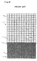
In the FT-CCD image sensor, the charge transfer paths 13
also perform as photoelectrical converters on an image
capturing area 15. Non-illustrated transparent electrodes are
attached above the charge transfer paths 13, and the charges
generated by the light incident through the transparent
electrode are transferred by changing the voltages applied to
the transparent electrodes. However, since charges are
continuously generated according to the incidence of the light
during the charge transfer, a light intercepted image
information storage area 16 comprising a CCD and corresponding
to one frame is provided in a lower part of the image capturing
area 15. At the time of image capturing, after exposure is
performed for a predetermined time, image information of one
frame is transferred from the image capturing area 15 to the
image information storage area 16 at an extremely high speed,
and the image information is read out to the outside of the image
sensor with leisure during the subsequent exposure. The FT-CCD
image sensor may be constructed of only a simple CCD. Moreover,
since light is incident also on the charge transfer paths 13,
the aperture efficiency is high, and therefore, it is
unnecessary to attach a microlens.
As described above, the FT-CCD image sensor is simpler
in structure than the IT-CCD image sensor because of unnecessity
of the input gates and the microlens. For this reason, early
CCD image sensors are of the FT-CCD type.
However, the FT-CCD image sensor, which captures incident
light through the transparent electrode, is low in the
sensitivity to the light in the wavelength range readily
absorbed by the transparent electrode. Normally, the
transparent electrode is made of polysilicon, and however thin
it may be, it largely absorbs blue light with short wavelengths .
In addition, since light is incident also during the charge
transfer, a so-called smearing, in which portions of an image
corresponding to high light-intensity are captured as
longitudinally elongated lines, is remarkable. To prevent the
smearing, it is necessary to take an artifice such as provision
of a mechanical or electrical high-speed shutter for
intercepting incident light during the charge transfer on the
front surface of the image sensor. Since these problems are
significantly improved in the IT-CCD image sensor, many of the
recent CCD image sensors are of the IT-CCD type or an improved
IT-CCD type.
With respect to the ISIS, the following image sensors are
both based on the IT-CCD type: a CCD image sensor shown in Fig.
19 developed by Kosonocky et al. (see F.W. Kosonocky et al.,
"360×360-Element Very-High Frame-Rate Burst-Image Sensor",
Digest of Technical Papers, ISSC 96, 1996, pp. 182-183); and
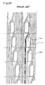
an image sensor shown in Figs. 20 and 21 that the present inventor
has already proposed (for example, see the above-mentioned
document of Takeharu ETOH and three others) . Specifically, in
these image sensors, each pixel has a large-size photodiode 115
and a CCD type recording portion 135 having a multiplicity of
small charge accumulation elements on a side of the photodiode
115. The photodiode 115 and the recording portion 135 are
interconnected by an input gate 114.
On the other hand, the FT-CCD type can be used as the basic
structure as shown in Fig. 22. In the FT-CCD image sensor shown
in Fig. 22, the entire area of the photoreceptive of the FT-CCD
image sensor of Fig. 18 is covered with an intercepting film
17, and in the intercepting film 17, windows 18 through which
light passes are formed so as to be staggered. Fifteen CCD
elements 19a to 19d below each window 18 can be used as image
information storage portions because they are covered with the
intercepting film. That is, the image information (charge) of
a first image generated at the CCD element 19a corresponding
to each window 18 is first accumulated in the CCD element 19b
immediately below the window 18. Then, the image information
of a second image generated at the CCD element 19a corresponding
to each window 18 is stored in the CCD element 19b immediately
below the window 18 at the same time when the first image
information is transferred to the CCD element 19c one row below.
By repeating similar processes, image information of fifteen
continuous frames is.stored in the CCD elements 19b to 19d.
After the shutter provided on the front surface of the image
sensor is closed, the image information is transferred one after
another in a vertical direction as in the normal FFT-CCD image
sensors, and the stored image information can be read out one
after another with leisure from a read-out circuit through a
horizontal CCD provided outside the photoreceptive area. When
the FT-CCD image sensor shown in Fig. 22 is employed as the basic
structure, the structure of the image sensor is sufficiently
simple compared to when the IT-CCD image sensor shown in Figs.
19 to 21 is employed as the basic structure, so that the
manufacturing cost can be reduced and noise can be suppressed.
In Fig. 22, the windows 18 are not arranged so as to form
squares. On the other hand, by arranging windows 18 as shown
in Fig. 23 and slanting the image capturing area with a gradient
of 4:1, the windows 18 form a square arrangement. In this case,
the basic axes 36 for designing the CCD and the orthogonal axes
37 of pixel arrangement interconnecting the centers of the
windows 18 obliquely intersect with a gradient of 4:1. With
the structure of Fig. 23, ISISs of orthogonal pixel arrangement
can be easily realized (see Japanese Laid-Open Patent
Application No. 2000-268010).
In high-speed image capturing, it is difficult to perform
image capturing in exact timing with the occurrence of a
phenomenon. For example, although the image sensor of Fig. 22
is capable of continuously image capturing fifteen images, when
image capturing is performed at intervals of 1/1,000,000 second
with the image sensor, image capturing is finished in
15/1,000,000 second. Therefore, a shift of timing of only
15/1,000,000 second makes it impossible to capture the target
phenomenon.
An example of means for solving this problem is serial
overwrite image capturing. The serial overwrite imaging is
started before the target phenomenon occurs, and finished
immediately after the occurrence of the phenomenon is confirmed.
The recorded image information is read out retroactively.
Comparing a method in which the occurrence of a phenomenon is
predicted and image capturing is started immediately before the
occurrence and a method in which image capturing is finished
after the occurrence of the phenomenon is confirmed, the latter
method is by far easier.
To realize this, for example, a drain 38 is provided in
the CCD element immediately above each window 18 as shown in
Fig. 23. The drains 38 are set so as to function during image
capturing and not to function during the information read-out
performed after image capturing.
The drains of normal CCD image sensors have roughly two
purposes. One is an overflow drain function of making the
excessive charge generated by excessive incident light
automatically overflow to the outside of the sensor in order
to prevent blooming that the excessive charge overflows to
surrounding pixels. The other is a simultaneous discharging
function of simultaneously discharging the temporarily stored
charge to the outside of the image sensor every charge transfer
stage. This function is employed, for example, for preventing
smearing due to incomplete charge transfer from the photodiode
to the CCD transfer path.
In ISISs, drain function for serial overwriting is further
added to these. Drains for serial overwriting are a kind of
simultaneous discharging drain in structure. However, while
electronic shutters and drains for smearing-prevention
function every charge transfer step, serial overwriting drains
in ISISs are activated immediately before the start of image
capturing, held activated during image capturing, and
deactivated immediately after the end of image capturing.
Since these drain functions are also very important in
ISISs, existing technologies regarding drains will be
concretely described. Examples of the drain structure include
a vertical drain structure and a horizontal drain structure.
In the vertical drain for the FT-CCD image sensor,
electrodes are provided above the CCD elements in the uppermost
row of the light intercepted image storage area 16 (39 in Fig.
18). A high voltage is applied to the electrode to thereby
transmit charge vertically below the CCD transfer paths,
resulting in that the charge is discharged from the rear surface
of the chip of the image sensor. The time necessary for merely
simultaneously transferring the image information of one frame
vertically downward within the image capturing area is
sufficiently short compared to the time for storing charges,
that is, the time necessary for reading out all of the image
information of one frame. The read-out needs long time because
image information is read out from the storage portion pixel
by pixel after the frame transfer. Therefore, charges can be
substantially simultaneously discharged by providing one row
of drains on the lower side of the photoreceptive area.
In the vertical drain for the IT-CCD image sensor, a high
negative voltage is applied to the chip rear surface, and charge
is discharged to the chip rear surface from a portion where a
potential barrier is weak, which portion is formed on the lower
surface of each photodiode.
On the other hand, in the horizontal drain, the drain is
disposed so as to adjoin the charge transfer path or the
photodiode, and a potential barrier is interposed therebetween
so that no charge flows into the drain in normal phases. When
a voltage is applied to the electrode disposed above the
potential barrier, the potential barrier decreases, so that
charge is discharged from the charge transfer path or the
photodiode into the drain on a side thereof. The charge
discharged into the drain is further discharged to the outside
of the sensor through an electrical wire disposed above the drain.
Alternatively, charge may be discharged from the chip rear
surface to the outside of the sensor through a portion,
immediately below the drain, where the potential barrier is
weak.
The drain can be used as an electronic shutter by turning
on and off the high voltage applied to the electrode for the
drain at an appropriate timing.
By providing a drain 38 in a CCD element 40 immediately
above each window 18 as shown in Fig. 23, the information of
the image captured at proceeding 16 steps is always continuously
discharged from the drain 38 to the outside of the image sensor
during image capturing, and the image information corresponding
to latest 15 frames is always recorded in a CCD accumulation
element.
After image capturing is finished, the shutter provided
on the front surface of the image sensor is closed, the
application of the drain voltage is stopped so that the drain
function is deactivated, and then, the image information stored
in the sensor is read out to the outside of the image sensor
by a normal CCD operation.
It should be noted that in case of the drain for serial
overwriting, a condition where the drain functions is
maintained during image capturing whereas a condition where the
drain does not function is maintained after image capturing is
finished. Concretely, electrodes for activating and
deactivating the drain function and power transmission means
for transmitting a voltage for the activation and deactivation
are newly required. The activation and deactivation are
performed not during image capturing but only immediately
before and after image capturing.
Normally, disposition of one layer of metal wires or
polysilicon wires on the surface of the image sensor is necessary
for operating the voltages transmitted to the electrode. By
applying the voltages to the drain electrodes through these
wires, charges are discharged from the rear surface of the image
sensor through the drain. The addition of one layer of wires
is an enormous load because the smaller the number of conductive
films for forming electrodes on the image sensor, the easier
the design and fabrication are.
In the case of the vertical drain, since the voltage is
normally applied from the chip rear surface, it is unnecessary
to further provide a wiring on the chip surface. However, since
the drains for these purposes including the drain for the
electronic shutter serving the three purposes of simultaneous
discharging, drain for overflow, and drain for serial
overwriting have different operations and positions of
placement from one another, it is difficult to realize all the
three functions only with the activation and deactivation of
the voltage applied to the chip rear surface and the voltage
level control. If the vertical drain control voltages can be
transmitted not only from the rear surface of the chip but also
from the upper surface thereof, it will become by far easy to
control these functions in combination.
Disclosure of Invention
The biggest problem of the image sensor of Fig. 22 is a
low aperture efficiency. In the case of Fig. 22, the aperture
efficiency is only 1/16, namely 6.25%. Further, when the number
of continuous images is set to 100 in the structure of Fig. 22,
the aperture efficiency is as low as 1% (1/100).
As a solution to this problem, it might be considered to
longitudinally elongate windows 55 as shown in Fig. 24. However,
this construction causes following two problems.
In the example of Fig. 24, CCD elements 56a to 56d
correspond to each window 55, and image information is not stored
until the charges generated at the four elements within the
exposure time are transmitted to CCD elements 56e to 56f of the
light intercepted image information storage portion. In other
words, the charges need to be transferred through four CCD
elements 56 to perform information storage for each one of images,
and four CCD elements 56 are required for storing image
information corresponding to each one of images. Therefor,
first, the transfer rate is 1/4 that in the case of Fig. 22.
Second, the number of images that can be stored is reduced to
1/4.
To solve this problem, it might be considered to provide
one elongated CCD element 72 for each elongated window 55 as
shown in Fig. 25 and transfer image information with a large
pitch. However, the too long CCD elements cause a problem in
the charge transfer. That is, as shown in Fig. 26, in normal
CCDs, when voltages are applied to adjoining electrodes 73, 74
and 75 in three steps, the potential distribution in the CCD
transfer path is not an ideal stepwise potential distribution
76 but is a potential distribution 77 having milder corner
portions of the steps. The effect of milder corner is called
a field fringing effect. Since this causes a potential gradient
in the transfer direction, the transfer rate is much higher than
in the case of the ideal stepwise potential distribution 76 where
the flat part is long.
In the CCD element 72 extremely elongated as shown in Fig.
25, a long flat part is formed in the potential gradient and
the time for the charge to move therethrough increases, thereby
the transfer rate decreases. Under some design conditions and
manufacture conditions, a part where a negative potential
gradient is caused in the charge transfer direction to trap
charges or a potential pocket is formed. In the case of Fig.
25, even if a small potential pocket may possibly be formed for
some reason, it is eliminated by the field fringing effect.
However, if the CCD pitch is too large, the length where the
field fringe functions relatively decreases, and such an effect
cannot be expected.
The other problem is how to newly add the drain for serial
overwriting in addition to the normal drain without
complicating the structure. If not only voltage from the chip
rear surface but also the drain control voltage can be
transmitted from the chip upper surface to activate and
deactivate the drain for serial overwriting, the design and the
operation of the drain will become easy.
In view of the above-mentioned problems of the
conventional image sensors, an object of the present invention
is to provide an image sensor, simple in structure and capable
of ultrahigh-speed image capturing based on the FT-CCD image
sensor.
To solve the problems, a first aspect of the present
invention provides an image sensor for ultrahigh-speed image
capturing comprising: a plurality of charge transfer paths each
constituted by a charge coupled device having a plurality of
elements and disposed parallel to each other; a plurality of
charge transfer electrodes intersecting the charge transfer
paths and provided for each element of the charge transfer paths;
an intercepting film covering the charge transfer paths and said
charge transfer electrodes so as to intercept an incident ray;
and a plurality of windows provided in the intercepting film
and allowing the incident ray to pass therethrough, wherein a
charge corresponding to an intensity of the incident ray is
generated at the element of the charge transfer path
corresponding to each window, and the generated charge is
transferred on the charge transfer path by voltages applied from
the charge transfer electrodes, and wherein each of the charge
transfer electrodes has a larger size in a charge transfer
direction at portions corresponding to the windows than that
at portions covered with the intercepting film.
Due to the frame transfer type, the image sensor for
ultrahigh-speed image capturing is simpler in basic structure
than the interline transfer type. Moreover, since each of the
charge transfer electrodes has a larger size in a charge transfer
direction at portions corresponding to the windows than that
at portions covered with the intercepting film, the aperture
efficiency is high. Further, charges can be transferred with
a large pitch, so that the charge transfer rate in the windows
or the image capturing speed is high. In addition, the number
of elements at each window decreases in inverse proportion to
the ratio of the width of the charge transfer electrode, the
number of elements necessary for accumulating one image
decreases, and the number of images that can be stored in the
sensor increases. As described above, in the image sensor for
ultrahigh-speed image capturing of the first aspect of the
present invention, the basic structure is simple, the aperture
efficiency is comparatively high, image capturing can be
performed at a higher speed, and a large number of continuous
frames can be captured.
Preferably, the portions of each charge transfer
electrode corresponding to the windows have upstream and/or
downstream sides in the charge transfer direction, the upstream
and/or downstream sides intersecting with respect to a
direction in which the charge transfer paths extend at angles
other than perpendicular to the direction.
In this case, since the length of the upper and/or the
lower sides increases and thereby the area where the field fringe
effect is caused increases, the transfer rate increases and a
potential pocket can be prevented from being caused in the
transfer path. By the upper and/or the lower side being
wedge-shaped, wavy, comb-shaped or the like, the side length
is extremely long, so that the area where the field fringe effect
is caused can be further increased.
Preferably, the intercepting film is made of a conductive
material. The image sensor further comprises: discharging
means provided for each charge transfer path, the number of said
discharging means being the same as the number of the windows
through which the charge transfer path passes; and a voltage
supply for supplying a drive voltage to the discharging means
through the intercepting film. The drive voltage is supplied
from the voltage supply to the discharging means to hold said
discharging means activated during image capturing, whereas the
supply of the drive voltage from said voltage applying means
to said discharging means is stopped to hold said discharging
means deactivated while the image capturing is stopped.
In this case, since the intercepting film is used as a
drain voltage control conductive film, introduction of a new
conductive film can be avoided. Specifically, since the
intercepting film has an extremely large area and a large
electric capacity, it is difficult to apply to this voltages
that suddenly change for electronic shuttering. Moreover,
since the intercepting film covers substantially the entire
area of the image capturing area, the image quality could be
affected if voltages that suddenly change would be applied every
step of transfer during image capturing. For this reason, the
intercepting film is normally not used as a power transmission
film. However, the drain for serial overwriting is always
activated during image capturing and deactivated for read-out
after image capturing is finished. The activation and
deactivation may be much slower than the operation of the
electrode for charge transfer during image capturing.
Moreover, since the drain is held activated during image
capturing, the voltage change at the time of activation and
deactivation does not affect the image quality. Consequently,
the intercepting film can be used as a conductive film for
transmitting drain voltages for serial overwriting, and it is
unnecessary to add a new conductive film, so that a combination
of three kinds of drains can be realized with a simpler
structure.
A second aspect of the present invention provides an image
capturing apparatus having one or a plurality of image sensors
for ultrahigh-speed image capturing having the above-described
characteristics. This image capturing apparatus enables
ultrahigh-speed and high-performance continuous image
capturing.
Brief Description of Drawings
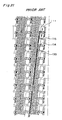
Fig. 1 is a schematic view showing an image capturing
apparatus having an image sensor of a first embodiment;
Fig. 2 is a partial front view showing an image capturing
area;
Fig. 3 is a sectional view taken on the line III-III of
Fig. 2;
Fig. 4 is a sectional view taken on the line IV-IV of Fig.
2;
Fig. 5 is a schematic view showing the arrangement of
charge transfer electrodes;
Fig. 6 is a partial enlarged front view of the surface
of a substrate;
Fig. 7 is a partial enlarged front view showing a charge
transfer electrode of the first layer;
Fig. 8 is a partial enlarged front view showing charge
transfer electrodes of the first and second layers;
Fig. 9 is a partial enlarged front view showing charge
transfer electrodes of the first, second, and third layers;
Fig. 10 is a partial enlarged front view showing the charge
transfer electrodes of the first, second, and third layers and
tungsten wires;
Fig. 11 is a partial enlarged front view showing the image
capturing area of an image sensor of a second embodiment;
Fig. 12 is a sectional view taken on the line XII-XII of
Fig. 11;
Fig. 13 is a partial enlarged front view showing the image
capturing area of an image sensor of a third embodiment;
Fig. 14 is a partial enlarged front view showing the
potential and the charge transfer path in the third embodiment;
Fig. 15 is a partial enlarged front view showing the image
capturing area of an image sensor of a fourth embodiment;
Fig. 16 is a partial enlarged view showing the potential
and the charge transfer path in the fourth embodiment;
Fig. 17 is a schematic view showing the interline transfer
CCD image sensor;
Fig. 18 is a schematic view showing the frame transfer
CCD image sensor;
Fig. 19 is a schematic view showing the ISIS image sensor;
Fig. 20 is a schematic view showing another ISIS image
sensor;
Fig. 21 is a schematic view showing the ISIS having the
CCD image information storage portion and the MOS amplification
read-out circuit for each pixel;
Figs. 22 to 25 are schematic views showing the frame
transfer CCD type ISISs; and
Fig. 26 is a schematic view showing the structure and the
principle of the three-phase-driven CCD.
Best Mode for Carrying Out the Invention
First Embodiment
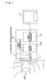
Fig. 1 shows the structure of the entire image capturing
apparatus. Light incident on a lens 101 passes through an
external shutter 102 and form an image on an image capturing
area 105 on a chip 104 of an image sensor 103 for ultrahigh-speed
image capturing. Charges are generated in accordance with the
intensity of the incident light during image capturing, and
excessive charges generated by excessive incident light are
discharged to ground through a drain wire 106. After image
capturing, the image information (in this case, charge) stored
in the image sensor through a read-out line 107 is converted
to digital information by an AD converter 108, and then stored
in a buffer memory 109. Then, the image information is
converted to image information of each of the continuous frames
by an image information processor 110, and then output to the
outside of the image capturing apparatus. This image
information can be viewed as a visible image through a monitor
11.
The image capturing apparatus also has a timing controller
112 for overall control. Further, the image capturing
apparatus has a constant voltage generator 113 for generating
several kinds of voltages necessary for controlling the CCD
image sensor.
Fig. 2 shows an enlargement of a part of the image
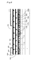
capturing area 105 of the image sensor. Fig. 3 is a cross-sectional
view of a transfer path in the charge transfer
direction, which shows a III-III cross section of Fig. 20. The
III-III cross section passes through a window. However,
tungsten wires 124 are actually situated within the same plane.
Fig. 4 shows a cross section in a direction perpendicular to
the transfer direction, which is a IV-IV cross section of Fig.
2.
The image capturing area is covered with an intercepting
film 14 made of aluminum, and windows 115 allowing light to pass
therethrough are formed.
Fig. 5 conceptually shows the elongated windows 115 and
charge transfer electrodes 116, 117 and 118 comprising
polysilicon electrodes. In the charge transfer electrodes 116,
117 and 118, the width (the size in the charge transfer
direction) of the portions 116a, 117b and 117c corresponding
to each window 115 is larger than that of the portions 116b,
117b and 118b covered with the intercepting film 114. In the
present embodiment, the width of the portions 116a, 117b and
117c corresponding to each window 115 is four times that of the
portions 116b, 117b and 118b covered with the intercepting film
114.
Figs. 6 to 10 concretely show the lamination structure
of the image sensor.
Fig. 6 shows the substrate from which the electrodes and
the intercepting film are removed. On the substrate, charge
transfer paths 122 (comprising n regions) and channel stops 123
(comprising p+ regions) are formed by diffusing or implanting
donor ions or acceptor ions.
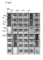
Figs. 7, 8 and 9 show statuses where the charge transfer
electrodes 116, 117 and 118 of the first, the second and the
third layers are successively laminated with insulator films
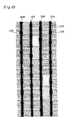
inserted between each of them. Fig. 10 shows a stasus where
the tungsten wires 124 for transmitting charge transfer
voltages to the charge transfer electrodes 116, 117 and 118 are
further provided. The tungsten wires 124 situated in a upper
layer and the charge transfer electrodes 116, 117 and 118
situated in lower layers are electrically interconnected in the
vertical direction through contact points 125. The above-described
Fig. 2 shows a status where the intercepting film 114
is further provided on the tungsten wires 124.
Charges corresponding to the intensity of the light
incident through the windows 115 are generated at elements 123a
of the charge transfer paths 123 corresponding to the windows
115 (see Figs. 5 and 6). By changing the voltage applied to
the charge transfer electrodes 116, 117 and 118, the charges
are transferred to CCD elements 123b situated in the light
intercepted portions (see Figs. 5 and 6) and stored as image
information. By repeating this operation, twelve continuous
images are stored at the point of time when the first image
information reaches the CCD element immediately above other
window immediately below the window. At this time, the external
shutter 102 is closed. Consequently, no new charges are
generated.
By performing a normal charge transfer operation of the
CCD transfer paths 123 under this condition, the stored charges
(image information) are transferred downward one after another,
and transmitted one by one to an output circuit (not shown)
through a horizontal CCD (not shown) provided in a lower part
outside the image capturing area. The image information is
converted to digital information by the AD converter 108 outside
the image sensor, stored in the buffer memory 109, and then
processed by the image information processor 110.
Since this image sensor for ultrahigh-speed image
capturing of the frame transfer type, it has a simpler basic
structure than the interline transfer type. Moreover, since
each of the charge transfer electrodes 116, 117, and 118 has
larger size in a charge transfer direction at portions 116a,
117a, and 118a corresponding to each of the windows than those
at portions 116b, 117b, and 118b covered with the intercepting
film 114, the aperture efficiently is high. Further, charges
can be transferred with a large pitch, so that the charge
transfer rate at the windows 115 or the image capturing speed
is high. In addition, since the number of elements 123a of the
CCCD transfer path 123 at each window 115 is one, the number
of elements 123b necessary for storing the charge corresponding
to one image is one, so that a multiplicity of frames of images
can be stored in the image sensor. As described above, in the
image sensor for ultrahigh-speed image capturing of the present
embodiment, the basic structure is simple, the aperture
efficiency is comparatively high, image capturing can be
performed at a higher speed, and a large number of continuous
frames can be captured.
Second Embodiment
In the image sensor for ultrahigh-speed image capturing
of a second embodiment of the present invention shown in Figs.
11 and 12, the size of the charge transfer paths 123 in a
direction perpendicular to the charge transfer direction is
increased at the windows 115. In correspondence therewith, a
gently curved portion 123c is provided on each charge transfer
path 123. Further, a drain 128 for serial overwriting is
provided on a right side of the charge transfer path 123
immediately above each window 115.
Moreover, the windows 115 are each fringed with a tungsten
layer 132 situated one layer below the aluminum intercepting
film 114. This construction is reducing a smearing phenomenon
caused by light or photoelectrons entering peripheral charge
transfer paths 123 from the windows 115.
In the image sensor of the present embodiment, since the
aperture efficiency is high compared to the first embodiment,
the sensitivity to light is dramatically improved.
Additionally, since serial overwriting is possible, it is
extremely easy to stop capturing in exact timing with the
occurrence of a phenomenon in ultrahigh-speed image capturing.
Moreover, the curved portion 123c assures a sufficient
space for disposing the drain 128 for overwriting read-out.
Consequently, a channel stop region 129 of a sufficient length
can be formed in a gap from the window on the left side of the
drain region, so that even if a high voltage is applied to the
drain electrode 132, the voltage can be prevented from adversely
affecting the charge transfer efficiency at the window 115 on
the left in the figure.
The basic difference from the first embodiment other than
the high aperture efficiency is that the drain 128 for serial
overwriting is provided. Therefore, this will be described.
In addition to the drain 128 for serial overwriting, a
normal vertical drain is provided on the lower surface of each
window 115 so as to perform as an overflow drain when the voltage
applied to the chip rear surface is low and function as a
simultaneous discharging drain when a high voltage is applied.
Description of this is omitted because it is a frequently used
structure.
Now, the drain 128 for serial overwriting will be
described in detail.
As shown in Fig. 12, a p-region 130 is provided in the
substrate so that the charges are prevented from escaping to
the rear surface by the potential barrier of the p-region 130.
A charge outflow path, so to speak, a hole 131 comprising an
n-region is formed below the drain 128, and the charges entering
the drain 128 are all automatically discharged from the chip
rear surface to the outside of the image sensor.
In overflow drains, instead of forming a complete.
electronic hole, the portion is a weak p-region so that when
charges are excessively stored, the potential barrier is
decreased (in other words, the electronic hole is formed) due
to the excessive charge storage and the charges are discharged
from the rear surface. When a high voltage is applied from the
rear surface, an electronic hole is also formed in the potential
barrier and the charges are simultaneously discharged.
As shown in Fig. 12, the drain electrode 132 is provided
on the upper surface of the drain 128 for serial overwriting.
At the time of serial overwriting, a high voltage is applied
to the drain electrode 132 by a voltage source 100, and the
potential barrier of the channel stop region 129 in a gap from
the charge transfer path 123 is decreased to thereby move the
charges to the side of the drain 128. Since a high voltage is
also applied to the drain 128 at this time, a weak p-region may
be provided also on the bottom of the drain for discharging
charges. In this case, a hole is also formed in the potential
barrier on the bottom by the voltage applied to the drain
electrode 132. Specifically, at the contact point 133, a
voltage is applied from the uppermost aluminum intercepting
film 114 to the drain electrode 132 through a light intercepting
layer 134 made of tungsten below the film 114.
The other functions and operations of the second
embodiment are the same as those of the first embodiment.
Specifically, the charge generated at each window 115 is
transmitted to the charge transfer path 123, and when reaching
the drain 128, automatically discharged to the outside of the
sensor. Therefore, as shown by the bold line in Fig. 11, the
charge transfer path 123 performs as the image information
storage region, and forty continuous frames of latest images
are always stored in the region.
When a target phenomenon to be capture occurs, the serial
overwriting operation is stopped as well as the external shutter
is closed, and then the application of the drain voltage is
stopped so that the charges can flow on the side of the charge
transfer path 123. After that, the accumulated image
information is read out to the outside of the image sensor with
leisure.
Since it is necessary for the serial overwriting drain
only to be activated immediately before image capturing and
deactivated immediately after image capturing as described
above, it is unnecessary to suddenly activate and deactivate
it during image capturing. Consequently, even if a voltage is
transmitted through the intercepting film 114 with a large
electric capacity, the delay in voltage transfer time does not
cause any problem. Moreover, since no sudden voltage change
occurs during image capturing, the image quality is not affected.
As described above, the intercepting film can be used as one
of the power supply layers, so that it is unnecessary to newly
add a power supply wire in an upper part of the image sensor
although an important function, serial overwriting, is added.
Third Embodiment
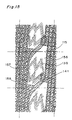
Fig. 13 shows a third embodiment of the present invention.
In the third embodiment, portions 136, 137 and 138 of the charge
transfer electrode corresponding to the window 115 are not
perpendicular but slanted to the charge transfer direction so
as to be wedged-shaped. Therefore, the length of the sides of
the portions 136, 137 and 138 where an electronic field fringe
is caused, that is, the length of overlapping portions 139 and
140 of the electrodes situated at upper and lower portions
thereof (on the upstream and the downstream sides in the charge
transfer direction) them are extremely long. Consequently,
the ratio of the area of a region 141 where the field fringe
effect is caused shown by the oblique lines in the figure with
respect to the area of the window 115 is high..
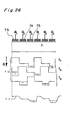
Fig. 14 shows the potential 150 and the charge transfer
direction 151 in the present embodiment. As is apparent from
Fig. 14, in the present embodiment, the portion of the charge
transfer path within the window 15 where a potential is flat
has decreased length, so that the charge transfer rate is
increased and the probability of incomplete charge transfer due
to a local potential pocket significantly decreases.
Fourth Embodiment
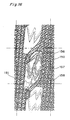
A fourth embodiment of the present invention shown in Fig.
15 is different from the second embodiment in the shapes of
portions 156, 157 and 158 of the charge transfer electrode
corresponding to the window 115. Specifically, overlapping
portions 139 and 140 of the electrodes on the upstream and the
downstream sides in the charge transfer direction are
respectively M-shaped and W-shaped. Therefore, compared to
the second embodiment in which the overlapping portions of the
electrode are linear, the length of the overlapping portions
139 and 140 is extremely long and the ratio of the area of the
field fringe caused region 141 with respect to the area of the
window 115 is extremely high, so that the field fringe effect
effectually works.
Fig. 16 shows the potential 150 and the charge transfer
direction 151 in the present embodiment. As is apparent from
Fig. 16, charges are transferred while spreading and
approaching in an X shape.
The present invention is not limited to the above-described
embodiments, but various modifications are possible.
For example, an overflow drain and an electronic shutter
function based on simultaneous discharging may be provided,
which is common in image sensors.
The transfer path in the windows may be originally
provided with a slight potential gradient to assist the field
fringe effect. For this, the impurity concentration may be
slightly increased in the transfer direction in the windows.
To form color images, a color filter array may be mounted.
To increase the substantial aperture efficiency, a micro
cylindrical lens may be mounted on each window. The on-chip
micro lens not only improves the substantial aperture
efficiency but also has an effect of converging light to a
central portion of the window and an effect of preventing light
or photoelectrons from diffusing from a peripheral portion of
the window to the transfer path adjoining the window.
The incident light is not limited to visible light. It
maybe different electromagnetic waves such as ultraviolet rays,
near-infrared rays or weak X rays, or may be particle beams such
as electron waves. However, in the case of weak X rays, electron
flows and the like, it is necessary to overlay an intercepting
film (not shown) made of a material that intercepts them. Since
ultraviolet rays are absorbed by polysilicon, it is necessary
that the polysilicon electrode be extremely thin or that the
charge drive electrode be made of a material transmitting
ultraviolet rays.
The metal layers are not necessarily made of aluminum or
tungsten. The intercepting layer may be made of tungsten, the
charge transfer drive voltage may be transmitted through an
aluminum wire, and both may be made of the same material.
The electrode configuration for improving the field
fringe effect is not limited to the ones of the third and the
fourth embodiments. In other words, it is minimum requirement
that the upstream and/or the downstream sides in the charge
transfer direction of the portions of the charge transfer
electrodes corresponding to the windows should intersect at an
angle not perpendicular to a direction in which the charge
transfer paths extend. Specifically, the electrodes may be
wedge-shaped, wavy or comb-shaped, so that the overlapping
portions of the electrodes are bent lines or curved lines of
the opposite phase or the same phase.
A thin n-region strip may be provided in the channel strap
regions surrounding the windows so that light and
photoelectrons diffusing from the periphery of the window to
the outside are converged and discharged from the drain.