TECHNICAL FIELD OF THE INVENTION
The present invention relates to an
electrochemical etching method and apparatus. In
particular, the present invention relates to a method and
apparatus in which an n-type silicon substrate is exposed
at its one surface to an electrolyte and at its opposite
surface to light, so that the substrate is formed with a
pore (hole) or trench (groove) of a certain size and shape
as an etching current flowing in the substrate is
controlled by the light. Also, the present invention
relates to a product, e.g., semiconductor device, made by
the use of the electrochemical etching method. It is to be
understood that the present invention is preferably
applicable to a method and apparatus for an electrochemical
etching for the formation of pores or trenches having a
diameter or width of 50nm or more in the n-type silicon
substrate. However, the present invention is not limited
by the size of the pore or trench.
BACKGROUND OF THE INVENTION
The Japanese Patent Publication No. 2,694,731
discloses an electrochemical etching system which uses
light to form small pores or trenches in an n-type doped
silicon substrate. The system has a holder for holding the
n-type doped silicon substrate (silicon wafer) with one
surface of the substrate contacted with an electrolyte
(hydrofluoricacid). Also, the holder retains an electrode
in the electrolyte so that the electrode opposes to the
silicon substrate. With this etching system, the silicon
substrate is positively biased and the electrode in the
electrolyte is negatively biased. The opposite side of the
silicon substrate away from the electrolyte is exposed to
light, causing holes in the silicon substrate. The holes
travel a boundary region of between the silicon substrate
and the electrolyte to resolve the boundary portion of the
silicon substrate. This means that an arrangement of a
masking barrier (coating) with one or more apertures (pits)
on the surface of the silicon substrate, adjacent to the
electrolyte, results in the formation of the pores or
trenches in the substrate portions, corresponding to the
apertures.
The Journal of Electrochemical Society, No. 140,
October 1993, pp. 2836-2843 discloses a back light device
for the illumination of silicon substrate. The light
device has a lamp for emitting light, an infrared filter
for removing infrared light from the emitted light, and a
convex lens for collimating the light emitted from the lamp.
Also, the Journal of Electrochemical Society, No.
137, February 1990, pp. 2836-2843 discloses an
electrochemical etching device which uses a 100W tungsten
lamp for the back light device.
Further, the Japanese Patent Publication No. 11-509644
discloses a system for manufacturing devices with
electrochemical etching unit. Another Japanese Patent
Publication No. 11-154737 discloses a manufacturing system
for incorporating a capacitance in the trench formed by the
electrochemical etching technique. Besides, the Journal of
Electrochemical Society, No. 137, February 1990, pp. 663-659
discloses an embodiment in which an aperture or trench
of 20 x 20 mm is formed in the silicon substrate by the
etching technique.
In order to mass-produce various devices using
the electrochemical etching system, the system is required
to make an even etching for the entire surface of a
relatively large silicon substrate with a diameter of three
inches or more, for example, and thereby form pores or
trenches of a certain size and shape at every portion of
the substrate.
Using the system disclosed in the Japanese Patent
Publication No. 2,694,731 and the 100W tungsten lamp in the
Journal of Electrochemical Society, No. 140, trials were
made to form pores of a certain diameter at every portion
in the three-inch silicon substrate. The etched silicon
substrate was viewed by the microscope, which showed that
pores were formed only in a limited part of the silicon
substrate. Also, the resultant pores have different sizes
and shapes. Although further trials were made under
different conditions in voltage, current and illumination,
uniform pores failed to be formed over the entire portion
of the silicon substrate.
Therefore, an object of the present invention is
to provide an electrochemical etching method and apparatus
capable of forming pores or trenches of a regular size
(depth and cross section) in a surface of n-type silicon
substrate having a diameter of three inches or more.
Another object of the present invention is to
provide devices, e.g., semiconductor device and sensors
such as acceleration sensor, manufactured through such
electrochemical etching method.
SUMMARY OF THE INVENTION
In order to attain the objects, an
electrochemical etching system according to one aspect of
the present invention has an illumination unit including a
light source for illuminating an illumination surface of an
n-type silicon substrate with an illumination of 10mW/cm2
or more. According to the embodiment, even for the silicon
substrate having a diameter of three inches or more, pores
and/or trenches to be formed in the silicon substrate
develops toward the illumination surface with a uniform
cross section. Also, the formed pore and/or trench has a
smooth surface.
In another aspect of the electrochemical etching
system of the present invention, on the illumination
surface of the silicon substrate, a ratio of the maximum
illumination to the minimum illumination is 1.69:1 or less.
With the arrangement, even for the silicon substrate having
a diameter of three inches or more, a constant etching
current flows in the silicon substrate, which ensures that
the formed pore and/or trench has a substantially constant
size (cross section and depth).
In another aspect of the electrochemical etching
system of the present invention, a reference electrode is
positioned in the electrolyte. A voltage detector with an
elevated impedance is electrically connected between the
reference electrode and the n-type silicon substrate. With
the arrangement, by controlling the voltage between the
reference electrode and the silicon substrate, the voltage
to be applied to the silicon substrate can be controlled.
In another aspect of the electrochemical etching
system of the present invention, an illumination unit has
an illumination controller for controlling an illumination
to the other surface of the silicon substrate. With the
arrangement, the size of the pore and/or trench to be
formed in the silicon substrate can be controlled.
In another aspect of the electrochemical etching
system of the present invention, the illumination
controller controls an amount of light emitted from the
light source. With the arrangement, the illumination to
the silicon substrate can be adjusted precisely.
In another aspect of the electrochemical etching
system of the present invention, the illumination
controller, which is positioned between the light source
and the silicon substrate, has a modulator for modulating
light emitted from the light source. With the arrangement,
where the light source is unable to control an amount of
light to be emitted therefrom, the illumination of the
silicon substrate can be controlled.
In another aspect of the electrochemical etching
system of the present invention, the system includes a
current detector for detecting a current applied from the
power source to the silicon substrate, and a circuit for
controlling the emitting light according to the current
detected by the current detector. With the arrangement,
the silicon substrate can be etched precisely.
In another aspect of the electrochemical etching
system of the present invention, the system includes a unit
for maintaining a stable condition of the hydrofluoricacid
(e.g., concentration and temperature). With the
arrangement, the hydrofluoricacid has a stable condition,
which in turn ensures the constant size of the pore and/or
trench formed in the silicon substrate.
In another aspect of the electrochemical etching
system of the present invention, the system has a metal
plate positioned on the other surface of the silicon
substrate. The metal plate is formed with a number of
regularly arranged openings so that light from the
illumination unit toward the silicon substrate is
transmitted therethrough. With the arrangement, the other
surface of the silicon substrate is illuminated uniformly,
which ensures the silicon substrate to be applied with a
constant voltage.
In another aspect of the electrochemical etching
system of the present invention, the metal plate is made of
electrically conductive material and is positioned adjacent
to the other surface of the silicon substrate. With the
arrangement, the power source and the silicon substrate are
electrically connected through the metal plate.
In another aspect of the electrochemical etching
system of the present invention, the metal plate is formed
integrally on the other surface of the silicon substrate.
With the electrochemical etching system, the metal plate is
formed precisely by the physical or chemical vapor
deposition and also the lithography used in the
manufacturing process for semiconductor. Also, the
openings can be formed with a great precision.
In another aspect of the electrochemical etching
system of the present invention, the metal plate is formed
independent of the silicon substrate. With the arrangement,
the manufacturing process of the silicon substrate can be
simplified.
An electrochemical etching method of the present
invention which includes the steps of making one surface of
an n-type silicon substrate into contact with an
electrolyte, illuminating the other surface of the silicon
substrate, and controlling an etching current by the
illumination to form a pore or trench in the one surface of
the silicon substrate is characterized in that the method
further comprises illuminating the the other surface of the
silicon substrate with an illumination of 10mW/cm2 or more.
In another aspect of the electrochemical etching
method, the method includes arranging a metal plate with a
number of regularly arranged openings on the other surface
of the n-type silicon substrate and illuminating the other
surface of the n-type silicon substrate through the
openings.
In another aspect of the electrochemical etching
method, a ratio of a maximum illumination to a minimum
illumination to the other surface of the silicon substrate
is 1.69:1 or less.
With the methods, even the silicon substrate
having a diameter of three inches or more is formed with a
substantially the same size pores and/or trenches in an
entire area of the substrate.
Another electrochemical etching method of the
present invention which has the steps of making one surface
of an n-type silicon substrate into contact with an
electrolyte, illuminating the other surface of the silicon
substrate, and controlling an etching current by the
illumination to form pores or trenches in the one surface
of the silicon substrate is characterized in that the
method further comprises a first step in which the other
surface of the silicon substrate is illuminated with a
first illumination of 10mW/cm2 or more to form the pores or
trenches extending toward the other surface of the silicon
substrate, and a second step in which, after the first step,
the other surface of the silicon substrate is illuminated
with another illumination higher than the first
illumination to extend the pores or trenches laterally to
connect the pores or trenches to each other. According the
method, the vertical pores can be connected at bottom
portion thereof to each other.
In view of above, according to the
electrochemical etching method of the present invention,
the shapes of the pores and/or trenches can be controlled
so precisely. Also, an enlarged substrate can be etched.
Then, the devices manufactured by the electrochemical
etching system has pores and/or trenches of which shape is
well controlled, ensuring a high performance and its
inexpensiveness.
BRIEF DESCRIPTION OF THE DRAWINGS
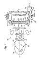
Fig. 1 is a schematic cross sectional view of an
electrochemical etching system according to the first
embodiment;
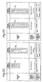
Figs. 2A to 2E are drawings, each of which
showing a cross sectional shape of a pore formed in the
silicon substrate, a diameter of the pore, and an
illumination in Experiment 2;
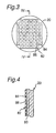
Fig. 3 is an exaggerated plan view of a grid
electrode layer positioned on a back surface of the silicon
substrate;
Fig. 4 is an enlarged cross sectional view taken
along lines V-V in Fig. 3, showing the grid electrode layer
in an exaggerated fashion;
Fig. 5 is a schematic cross sectional view of the
electrochemical etching system according to the second
embodiment;
Fig. 6 is a schematic cross sectional view of the
electrochemical etching system according to the third
embodiment;
Fig. 7 is a schematic cross sectional view of the
electrochemical etching system according to the fourth
embodiment;
Fig. 8 is a schematic cross sectional view of the
electrochemical etching system according to the fifth
embodiment;
Fig. 9 is a schematic cross sectional view of the
electrochemical etching system according to the sixth
embodiment;
Fig. 10 is a schematic plan view of the grid
electrode plate for use in the electrochemical etching
system according to the seventh embodiment;
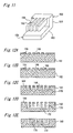
Fig. 11 is a schematic plan view of an
acceleration sensor manufactured by the electrochemical
etching method according to the eighth embodiment;
Figs. 12A to 12E are drawings for describing
processes of the electrochemical etching method according
to the eighth embodiment;
Fig. 13 is a perspective view of an optical guide
member manufactured by the electrochemical etching method
according to the ninth embodiment; and
Figs. 14A to 14E are drawings for describing
process of the electrochemical etching method according to
the ninth embodiment.
DETAILED DESCRIPTION OF THE PREFERRED EMBODIMENTS
With reference to the drawings, descriptions will
be made to the preferred embodiments of the present
invention. Like reference numerals indicate like parts
throughout the drawings.
FIRST EMBODIMENT
Referring to Fig. 1, there is shown an
electrochemical etching system for an n-type silicon
substrate (silicon wafer) 10 according to the first
embodiment of the present invention. The etching system 10
includes an etching bath 12 for receiving an etching
electrolyte 14 of 5wt% hydrofluoricacid. A surface portion
of the etching bath 12, making a contact with the etching
electrolyte 14, is coated with an appropriate material,
e.g., polytetrafluoroethylene, that resists against
hydroflluoricacid. Alternatively, the etching bath 12 may
fully be made of material that resists against
hydroflluoricacid.
The etching bath 12 is formed at its wall 16 with
a round opening 18 for receiving a disc-like n-type silicon
wafer 20 therein. The wall 16 includes an annular flange
22 running along an inner periphery of the opening 18 and
projecting toward a center of the opening 18. In order to
secure the silicon substrate 20, a fixing ring 24 is
provided behind the substrate 20 to force the silicon
substrate 20 against the annular flange 22. Preferably, a
suitable sealing member, e.g., O-ring 26, is positioned
between the annular flange 18 and the silicon substrate 20
to prevent the electrolyte 14 from leaking therebetween.
One electrode 28 (cathode) is provided in the
electrolyte 14 so that it opposes to the silicon substrate
20 received in the opening 18. The silicon substrate 20
is used for the other electrode or anode. The electrode
(cathode) 28 and the silicon substrate (anode) 20 are
electrically connected to a DC power supply 30, so that a
suitable voltage can be applied between the electrode
(cathode) 28 and the silicon wafer (anode) 20. Preferably,
the fixing ring 24 for fixing the silicon substrate 20 in
position is made of an electrically conductive material for
the electrical connection between the silicon substrate 20
and the power source 30.
A surface 32 of the silicon wafer 20 adjacent to
the electrolyte 14 is coated with a masking barrier or
resist mask 34. The masking barrier 34 is made of a
suitable masking material, e.g., silicon nitride, platinum,
or gold, which is deposited by a suitable deposition
technique, e.g., chemical or physical vapor deposition.
The surface 32 of the silicon substrate is formed with one
or more pits or apertures 36 corresponding to an etching
pattern of the silicon substrate 20. This causes that
etching or resolving proceeds at the associated portions of
the silicon substrate exposed in the pits 36 toward the
opposite surface 38 of the silicon substrate, forming pores
or trenches in silicon substrate. Preferably, the pits 36
are formed by a suitable technique such as wet etching, dry
etching, and laser machining.
The etching system 10 includes an electrolyte
unit 40. The electrolyte unit 40 has a circulation passage
or tube 42 which is fluidly connected at its opposite ends
to the etching bath 12. The circulation passage 42 has a
pump 44 for pumping the electrolyte 14 through the
circulation passage 42, a filter 46 for removing foreign
substances from the electrolyte 14 running in the
circulation passage 42, a buffer 48 for maintaining a
constant amount of electrolyte 14 in the etching bath 12,
and a thermostat 50 for maintaining a temperature of
electrolyte 14 in the etching bath 12 constant. The
electrolyte unit 40 maintains a necessary quality of the
electrolyte 14 in the etching bath 14, ensuring a stable
etching of the silicon substrate 20 described below.
The etching system 10 further includes a back
light unit 52. The back light unit 52 is used to
concentrate holes generated in the silicon substrate 20 at
a leading edge of each pore where the further etching or
resolving of the substrate proceeds locally. For this
purpose, the back light unit 52 has an illumination source
or lamp 56, e.g., tungsten lamp, located on an central axis
54 of the circular opening 18 of the etching bath 12 and a
semi-oval reflector or mirror 58 of which opening 60 is
directed toward the circular opening 18 of the etching bath
12. A curvature of the mirror 58 is determined so that
light from the lamp 54 is reflected by the mirror 58 to
focus on a certain point (focal point) 62 on the axis 54.
A collimator lens 64 is opposed to the opening 60 of the
mirror 58 so that light from the mirror 58 is collimated by
the collimator lens 64. Another convex lens 66 is
positioned between the collimator lens 64 and the silicon
substrate 20 so that the collimated light is then extended
toward the silicon substrate 20, causing the back surface
of the silicon substrate, away from the electrolyte, to be
illuminated. Preferably, as shown in Fig. 1, a filter 68
is provided to remove a part of light, e.g., light having a
wavelength of 1.1µm or more, in order to prevent the
silicon substrate 20 from being overheated. Also, a
suitable fan or fans 70 may be provided adjacent to the
silicon substrate 20 for the cooling of the substrate.
Hereinafter, a brief description will be made to
the operation of the etching system 10 so constructed. In
operation, the silicon substrate 20 is secured in the
opening 18 of the etching bath 12. Then, the electrolyte
14 is filled in the etching bath 12. Then, the power
source 30 applies a certain voltage between the electrode
28 and the silicon substrate 20, and the illumination lamp
52 illuminates the back surface 38 of the silicon substrate
20. This causes holes in the silicon substrate to
concentrate at the portions of the silicon substrate,
exposed in the pits 36. As a result, a local etching or
resolving is initiated at each of the exposed portions and
then advanced straightly toward the opposite back surface
38 of the silicon substrate 20.
EXPERIMENT 1
Tests were made to evaluate a relation between an
illumination and configurations of the resultant pores.
1. Conditions
Test conditions were as follows:
The illumination was measured on the back surface of
the silicon substrate, using a Power Meter commercially
available from Advantest Corporation under the name of
Light Multi-Power Q8221, with a calibrated wavelength of
760nm.
iv. Voltage (Voltage applied between the electrode and the
silicon substrate)
2.0 volts and 4.0 volts v. Etching period
20 minutes
2. Evaluation
The etched silicon was cut and the its cross section,
in particular, the longitudinal cross section of pore, was
observed using a microscope. Using the microscopic
photographs, diameters of several pores were measured at a
certain distance of 5µm away from the front surface of the
silicon substrate.
3. Results
The test results are shown in the following Table 1:
| Illumination | Voltage Applied |
| (mW/cm2) | 2.0 volts | 4.0 volts |
| 0 | C | C |
| 5 | B | B |
| 10 | A | A |
| 20 | A | A |
| 30 | A | A |
| 50 | A | A |
| 100 | A | A |
| 200 | A | A |
In Table 1, evaluation A, B and C means as
follows:
4. Conclusion
The table 1 shows that the illumination affects
on the resultant pore configuration significantly. Also
revealed is that, in order to form a pore running
straightly toward the back surface of the substrate and
having an even cross section, the illumination should be
set 10mW/cm2 while keeping a suitable voltage between the
electrode and the silicon substrate.
In order to provide the illumination of 10mW/cm2
for the entire back surface of the silicon substrate, a
1.0KW xenon arc lamp is advantageously used for the light
source. Anther lamp such as tungsten lamp or mercury lamp
can be used instead provided that it ensures the
illumination of 10mW/cm2.
An application of an increased voltage between
the silicon substrate and the electrode may result in pores
having a diameter of 50nm or more in the silicon substrate.
However, this etching is different from the electrochemical
etching technique according to the present invention.
EXPERIMENT 2
Tests were made to evaluate an affect of
illumination on the configuration of pores in the silicon
substrate.
1. Conditions
Test conditions were as follows:
2. Evaluation
The etched silicon was cut and the its cross section,
in particular, the longitudinal cross section of pore, was
observed using a microscope. Using the microscopic
photographs, diameters of several pores were measured at a
certain distance of 5µm away from the front surface of the
silicon substrate.
3. Results
The test results are shown in Figs. 2A-2D. As shown
in the tables in the drawings, where a ratio (IMAX/IMIN) of
the maximum illumination IMAX and the minimum illumination
IMIN being 1.96 and 2.25, the configurations of pores formed
at the maximum illumination point and the minimum
illumination point were quite different from each other.
Also, the diameter of the pore at the maximum illumination
was extended toward the leading end of the pore.
Where the ratio of the maximum illumination and
the minimum illumination being 1.69, although the pores had
separate diameters slightly different from the other, they
have substantially the same depth. Also, the pores had
substantially smooth surfaces. Likewise, where the ratio
of the maximum illumination and the minimum illumination
being 1.21, the pores had substantially the same size and
they had smooth surfaces.
4. Conclusion
The result of experiment 2 shows that, even for
the silicon substrate having a diameter of 3 inches or more,
pore or trenches having substantially the same diameter are
formed at every place in the silicon substrate provided
that the ratio of the maximum illumination and the minimum
illumination is 1.69 or less.
IMPROVEMENTS/MODIFICATION
Figs. 3 and 4 show the silicon substrate 20. The
silicon substrate 20 has an n+ layer 80 in the back surface
38 opposing to the back light unit 52, in which ion is
injected using a known donor ion injection technique. A
metal layer (metal plate or grid metal layer) 82, made of
conductive material, is provided on the n+ layer 80.
Preferably, as best shown in Fig. 3, the metal layer 82 is
in the form of grid. Preferably, the grid metal layer 82
is made by depositing the conductive material through a
film formation technique such as chemical or physical vapor
deposition and then forming openings 86 so that a grid 84
remains between openings through a technique such as
photolithography.
The grid layer 82 so defined has a smaller
contact resistance against the n-type silicon substrate 20,
which allows a constant voltage to be applied through the
grid metal layer 20 to the entire portion of the silicon
substrate 20 which is in contact with the grid metal layer
82.
Although the opening 86 in the grid 84 is not
limited to a specific size, it should be smaller than the
thickness of the silicon substrate 20. This is because
that the illumination to the silicon substrate 20 decreases
with the increase of the width of the grid 84 between the
openings 86, which reduces the concentration of the hole in
the silicon substrate 20.
Studies conducted by the inventors revealed that,
where each line of the grid 84 has a width of 10µm and its
interval is 90µm, a constant voltage can be applied to
every portion of the silicon substrate 20, overcoming the
problems caused by the reduction of illumination.
Preferably, when using electrode 28 made of
platinum, the voltage between the electrode 28 and the
silicon substrate 20 is determined so that the n-type
silicon substrate 20 is biased higher than the electrode 28
by +1 to +4 volts. This causes pores and trenches to be
generated in the substrate more efficiently.
SECOND EMBODIMENT
Referring to Fig. 5, there is shown another
electrochemical etching system 90 according to the second
embodiment of the present invention. In this etching
system 90, the back light unit 92 includes a plurality of
lamps 94 arranged in a lattice on a plane perpendicular to
the central axis of the silicon substrate 20 (or on a plane
parallel to the silicon substrate 20). With this etching
system 90, the back surface of the silicon substrate 20 is
illuminated uniformly. Also, the plurality of lamps 94 can
be positioned easily so that the ratio of maximum/minimum
illumination ratio takes 1.69 or less.
THIRD EMBODIMENT
Referring to Fig. 6, there is shown another
electrochemical etching system 100 according to the third
embodiment of the present invention. In this etching
system 100, a reference electrode 102, which is positioned
in the electrolyte 14 between the silicon substrate 20 and
the electrode 28, is electrically connected through a
voltage meter 104 to the power source 30 for measuring the
voltage to be applied to the silicon substrate 20.
Preferably, the voltage meter 104 is designed to provide an
elevated impedance between the reference electrode 20 and
the silicon substrate 20. In operation of the etching
system 100, the power source 30 is controlled so that a
constant voltage is applied to the voltage meter 104,
ensuring a constant current to flow between the silicon
substrate 20 and the electrode 28.
Preferably, the reference electrode 102 is
positioned as close as possible to the silicon substrate 20
while leaving a small gap therebetween. This minimizes the
electric resistance of the electrolyte 14 between the
reference electrode 102 and the silicon substrate 20. Also,
this ensures that the voltage applied to the silicon
substrate 20 is detected precisely and, thereby, that the
configuration of the pore/trench is well controlled.
FOURTH EMBODIMENT
Referring to Fig. 7, there is shown another
electrochemical etching system 110 according to the fourth
embodiment of the present invention. In this etching
system 110, the illumination lamp 56 is electrically
connected to a voltage controller 112 for changing the
illumination to the silicon substrate 20. With this
etching system 110, an etching current supplied from the
power source 30 to the silicon substrate 20 changes in
proportion to the illumination. Therefore, by changing the
voltage applied to the lamp 56 by the voltage controller
112 and, thereby, the illumination to the silicon substrate
20, the size of the resultant pore and/trench can be varied.
Also, a pore and/or trench with an enlarged cavity or cross
section at its leading portioin can easily be formed by
forming a pore or trench having a uniform cross section and
then increasing the illumination and the etching current.
FIFTH EMBODIMENT
Referring to Fig. 8, there is shown another
electrochemical etching system 120 according to the fifth
embodiment of the present invention. This etching system
120 has two polarizing devices or filters 122 and 124
between the convex lens 66 and the filter 68. Also, one of
the two polarizing filters 122 and 124 is supported for
rotation about a central axis 54 of the silicon substrate
20 relative to the other in order to control a quantity of
light passing through the two polarizing filters 122 and
124 and thereby the illumination to the silicon substrate
20. This means that simply by rotating the rotatable
filter, rather than controlling the illumination of the
lamp 56, the size of the pore and trench formed in the
silicon substrate can be controlled.
In this embodiment, the rotatable polarizing
filter may be mechanically connected to a drive unit (e.g.,
motor) 126 for rotating the polarizing filter about the
central axis 54, which in turn connected to the controller
128. This allows the controller 128 to control the drive
unit 126, positioning the polarizing filter in a desired
position.
SIXTH EMBODIMENT
Referring to Fig. 9, there is shown another
electrochemical etching system 130 according to the fifth
embodiment of the present invention. In this etching
system 130, the illumination lamp 56 is electrically
connected to a voltage controller 132 for controlling the
voltage applied to the lamp 56. A current detector or
amperemeter 134 is electrically connected between the power
source 30 and the silicon substrate 20 for detecting the
etching current supplied from the power source 30 to the
silicon wafer 20. The voltage controller 132 and the
amperemeter 134 are electrically connected to each other
through a feedback circuit 136.
With this etching system 130, the feedback
circuit 136 reads the etching current detected by the
amperemeter 134, and then transmits a corresponding signal
to the voltage controller 132 for controlling the
illumination to the silicon substrate 20. This in turn
alters the etching current, changing the shape of the pore
and/or trench. As described above, according to the
etching system 130, by controlling the illumination, the
etching current can be kept constant to form pores
and/trenches in a precise manner.
The feedback circuit 136 may be electrically
connected to the position controller of the polarizing
filter. In this instance, the polarizing filter is rotated
according to a signal from the feedback circuit 136,
allowing the illumination to the silicon substrate to be
controlled in a precise manner.
SEVENTH EMBODIMENT
Although in the first embodiment the grid metal
layer is integrally formed on the back surface of the
silicon substrate, it may be formed as an independent
member capable of being separated from the silicon wafer.
Specifically, Fig. 10 shows a grid metal plate 140 made of
an electrically conductive material. Preferably, as
described above, the size of the grid 142 and the opening
144 in the grid metal plate 140 are determined so that the
size of the grid 142 is smaller than the thickness of the
silicon substrate.
The grid metal plate 140 is sealingly attached on
the back surface of the silicon substrate and then secured
by a suitable fixing member. Preferably, the grid metal
plate 140 is manufactured integrally with the fixing ring
which is used for fixing the silicon substrate to the
etching bath. This facilitates the fixing of the grid
metal plate 140 to the silicon substrate without any
difficulty.
EIGHTH EMBODIMENT
Fig. 11 shows an accelerometer or acceleration
sensor 150 manufactured by the use of the electrochemical
etching system of the present invention. The acceleration
sensor 150 has a base 152. The base 152 has a wall 154
extending vertically from the base 152. The wall 154 has a
plurality of spaced, cantilever-like, deformable portions
156 extending in parallel from the wall 154. The base 152,
wall 154, and deformable portions 156 are formed in a
single product 158 by shaping a silicon substrate using the
electrochemical etching technique of the present invention.
Each of the deformable portions 156 supports a strain
member, e.g., piezoelectric member or resistance 160, for
measuring a deformation of the deformable portion 156.
In operation, when any acceleration is acted on
the acceleration sensor 150, each of the deformable
portions 156 sags toward a direction opposing to the
acceleration. Then, the deformation of the deformable
portion 156 is detected from the change of resistance of
the piezoelectric member 160.
Referring to Figs. 12A to 12E, a process for
manufacturing the product 158 from the silicon substrate
will be described below. At first, prepared is an n-type
silicon substrate 162 with a certain thickness (see Fig.
12A). Then, a silicon nitride layer 164 is deposited on
one surface of the n-type silicon substrate 162 by the
chemical vapor deposition, for example. Next, portions of
the nitride layer are removed by the photolithography to
form patterning grooves 166 for etching the corresponding
portions of the silicon substrate to define the tip end
surface and the side surfaces of each of the deformable
portions 156. Subsequently, as shown in Fig. 12B, portions
of the silicon substrate, exposed in the patterning grooves
166, are etched by wet etching with a suitable alkaline
solution or reactive ion etching, for example, forming pits
168 from which the subsequent etching will be initialized.
The silicon substrate 162 with the nitride
silicon layer 164 is mounted on the electrochemical etching
system for its etching. At this moment, the silicon
substrate 162 is positioned so that the nitride silicon
layer 164 and the patterning grooves 166 opposes to the
etching electrolyte, i.e., hydrofluoricacid, and light is
illuminated to the back surface of the silicon substrate
162. The opposing electrode may be made of platinum.
The etching is performed in two steps. In the
first etching process, the platinum electrode and the
silicon substrate are biased so that the silicon substrate
is +2 volts higher than the platinum electrode. An average
illumination is set 70 W/cm2. The ratio of the maximum and
minimum illumination is set 1.69 or less. With this
condition, as shown in Fig. 12C, the silicon substrate 162
is etched to form vertical trenches 1·70 extending toward
the back surface of the silicon substrate 162,
corresponding to the patterning grooves 166. This first
etching process is continued for about 15 minutes.
In the second etching process, the average
illumination is increased to 200 W/cm2. Other conditions
are the same as those in the first etching process. As a
result, as shown in Fig. 12D, the leading end portion of
the vertical trenches 170 are extended laterally to form
lateral trenches 172, which results in the individual
deformable portions 156.
Finally, if necessary, the nitride silicon layer
164 is removed by etching, for example. Although one
product 158 is illustrated in Figs. 11 and 12A-12E for
clarity, a number of products 158 may be formed
simultaneously in one silicon substrate. In this instance,
after the piezoelectric resistances are provided on the
deformable portions, the acceleration sensors are divided
into pieces by dicing, for example.
Also, for the acceleration sensor, a typical
thickness of the deformable portion may be about 20µm.
However, it may be varied to obtain different acceraletion
sensors with different sensitivities. Simply by
controlling the etching period for the first and/or the
second etching, the thickness can be varied.
As described above, by the use of the
electrochemical etching method, a number of sensors can be
manufactured in one wafer. Also, a product with a
complicated structure can be made through one etching
including first and second etching processes, reducing the
manufacturing time and cost of the products considerably.
Naturally, the above etching is used in the
manufacturing not only of the acceleration sensors but also
of other devices including products with a complicated
shape.
NINTH EMBODIMENT
Fig. 13 shows a light conducting member 180
manufactured by the electrochemical etching system of the
present invention. The light conducting member 180 has a
product 182 made of one n-type silicon substrate. In this
embodiment, the product 182 is in the form of substantially
rectangular plate including a first region or lattice
structure 184 in which a number of small pores are formed
at regular intervals (e.g., in a lattice) and a light
conducting passage 186 running across the lattice structure
184. Although the light conducting passage 186 extends in
the form of L from one side surface 188 to another side
surface 190, it is not limited thereto.
The light conducting member 180 uses a feature of
the lattice structure 188, which selectively eliminates
light having a wavelength corresponding to the pitch of the
pores. The feature is introduced in the Journal of Applied
Physics, Vol. 66 25, pp. 3254-3256. With this light
conducting member 180, when light 192 is guided into an one
end of the light conducting passage 186 in the side surface
188, light 194 except for a part of light having a
wavelength corresponding to the size of the lattice is
transmitted through the lattice structure 184. The part of
light 196, which is prohibited from passing through the
lattice structure 184, is guided by the light conducting
passage 186 and then fed out of the other end of the
passage 186 in the side surface 180. As described above,
only the part of light having the specific wavelength is
selectively extracted.
Referring next to Figs. 14A to 14E, descriptions
will be made to a process for manufacturing the product 182
from a silicon substrate. First, an n-type silicon
substrate 200 having a certain thickness is prepared (Fig.
14A). Then, a nitride silicon layer 202 is deposited on
one surface of the n-type silicon substrate 200 by the
chemical vapor deposition (CVD), for example. Next,
portions of the layer, corresponding to the pores in the
lattice structure 184, are removed by a photolithography,
for example, forming a pattern of pores. In the drawing,
concave portions formed by the removal process are
indicated at 204. An interval of the concave portions 204
is about 700µm. However, the interval may vary depending
upon a wavelength of light to be separated. Subsequently,
as shown in Fig. 14B, by an wet etching using alkaline
solution or a reactive etching, parts of the silicon
substrate exposed in the concave portions are formed with
pits 206 where a subsequent etching will be initiated
therefrom.
The silicon substrate 200 with the nitride
silicon layer 202 is mounted on the electrochemical etching
system for the etching of the silicon substrate 200. At
this moment, the silicon substrate 200 is positioned so
that the nitride silicon layer 202 and the concave portions
204 oppose the electrolyte, i.e., hydrofluoricacid, so that
light is illuminated to the opposite surface of the silicon
substrate 200. Platinum is used for the opposing electrode.
The etching is performed in two steps. In the
first etching process, the platinum electrode and the
silicon substrate are biased so that the silicon substrate
is +2 volts higher than the platinum electrode. An average
illumination is set 40 W/cm2. The ratio of the maximum and
minimum illumination is set 1.69 or less. This causes that,
as shown in Fig. 14C, the vertical pores 208 each having a
depth of about 100µm are extended in the silicon substrate
200, corresponding to the pore pattern.
Before the second etching process, the silicon
substrate 200 is removed from the electrochemical etching
system. As shown in Fig. 14D, the nitride silicon layer is
eliminated from the silicon substrate 200 and then a metal
layer, e.g., aluminum layer 210, is deposited by the
physical or chemical vapor deposition, e.g., sputtering,
instead. Also, a part of the aluminum layer corresponding
to the light conducting passage 186 is removed.
In the second etching process, portions of the
silicon substrate 200, not coated with the aluminum layer
210, are etched by the reactive ion etching. This results
in the lattice structure 184 with pores 208 and the light
conducting passage 186 running across the lattice structure
184.
With the light conducting member 180 in which
pores are formed in a lattice, light having a wavelength of
1.5µm is selectively extracted. Another light conducting
member capable of extracting light with a different
wavelength is obtained by changing the interval and/or the
size of the pores. Also, by the use of the above-described
electrochemical etching method, another light conducting
member having a larger area can be obtained.
Although, there has been described several
embodiments in accordance with the present invention, it
will be appreciated that the invention is not limited
thereto. Accordingly, any and all modifications,
variations, or equivalent arrangements which may occur to
those skilled in the art should be considered to be within
the scope of the present invention as defined in the
appended claims.