EP1219422B1 - Einbauen von Silizium Brücken in Tintenkanäle eines Cmos/Mems integrierten Tintenstrahldruckkopfs und dazugehöriges Herstellungsverfahren - Google Patents
Einbauen von Silizium Brücken in Tintenkanäle eines Cmos/Mems integrierten Tintenstrahldruckkopfs und dazugehöriges Herstellungsverfahren Download PDFInfo
- Publication number
- EP1219422B1 EP1219422B1 EP01130219A EP01130219A EP1219422B1 EP 1219422 B1 EP1219422 B1 EP 1219422B1 EP 01130219 A EP01130219 A EP 01130219A EP 01130219 A EP01130219 A EP 01130219A EP 1219422 B1 EP1219422 B1 EP 1219422B1
- Authority
- EP
- European Patent Office
- Prior art keywords
- ink
- nozzle
- print head
- ink jet
- silicon substrate
- Prior art date
- Legal status (The legal status is an assumption and is not a legal conclusion. Google has not performed a legal analysis and makes no representation as to the accuracy of the status listed.)
- Expired - Lifetime
Links
Images


Classifications
-
- B—PERFORMING OPERATIONS; TRANSPORTING
- B41—PRINTING; LINING MACHINES; TYPEWRITERS; STAMPS
- B41J—TYPEWRITERS; SELECTIVE PRINTING MECHANISMS, i.e. MECHANISMS PRINTING OTHERWISE THAN FROM A FORME; CORRECTION OF TYPOGRAPHICAL ERRORS
- B41J2/00—Typewriters or selective printing mechanisms characterised by the printing or marking process for which they are designed
- B41J2/005—Typewriters or selective printing mechanisms characterised by the printing or marking process for which they are designed characterised by bringing liquid or particles selectively into contact with a printing material
- B41J2/01—Ink jet
- B41J2/015—Ink jet characterised by the jet generation process
- B41J2/02—Ink jet characterised by the jet generation process generating a continuous ink jet
- B41J2/03—Ink jet characterised by the jet generation process generating a continuous ink jet by pressure
- B41J2002/032—Deflection by heater around the nozzle
-
- B—PERFORMING OPERATIONS; TRANSPORTING
- B41—PRINTING; LINING MACHINES; TYPEWRITERS; STAMPS
- B41J—TYPEWRITERS; SELECTIVE PRINTING MECHANISMS, i.e. MECHANISMS PRINTING OTHERWISE THAN FROM A FORME; CORRECTION OF TYPOGRAPHICAL ERRORS
- B41J2202/00—Embodiments of or processes related to ink-jet or thermal heads
- B41J2202/01—Embodiments of or processes related to ink-jet heads
- B41J2202/13—Heads having an integrated circuit
-
- B—PERFORMING OPERATIONS; TRANSPORTING
- B41—PRINTING; LINING MACHINES; TYPEWRITERS; STAMPS
- B41J—TYPEWRITERS; SELECTIVE PRINTING MECHANISMS, i.e. MECHANISMS PRINTING OTHERWISE THAN FROM A FORME; CORRECTION OF TYPOGRAPHICAL ERRORS
- B41J2202/00—Embodiments of or processes related to ink-jet or thermal heads
- B41J2202/01—Embodiments of or processes related to ink-jet heads
- B41J2202/16—Nozzle heaters
-
- B—PERFORMING OPERATIONS; TRANSPORTING
- B41—PRINTING; LINING MACHINES; TYPEWRITERS; STAMPS
- B41J—TYPEWRITERS; SELECTIVE PRINTING MECHANISMS, i.e. MECHANISMS PRINTING OTHERWISE THAN FROM A FORME; CORRECTION OF TYPOGRAPHICAL ERRORS
- B41J2202/00—Embodiments of or processes related to ink-jet or thermal heads
- B41J2202/01—Embodiments of or processes related to ink-jet heads
- B41J2202/22—Manufacturing print heads
Definitions
- This invention generally relates to the field of digitally controlled printing devices, and in particular to liquid ink print heads which integrate multiple nozzles on a single substrate and in which a liquid drop is selected for printing by thermo-mechanical means.
- Ink jet printing has become recognized as a prominent contender in the digitally controlled, electronic printing arena because, e.g., of its non-impact, low noise characteristics and system simplicity. For these reasons, ink jet printers have achieved commercial success for home and office use and other areas.
- Ink jet printing mechanisms can be categorized as either continuous (CIJ) or Drop-on-Demand (DOD).
- U.S. Patent No. 3,946,398 which issued to Kyser et al. in 1970, discloses a DOD ink jet printer which applies a high voltage to a piezoelectric crystal, causing the crystal to bend, applying pressure on an ink reservoir and jetting drops on demand.
- Piezoelectric DOD printers have achieved commercial success at image resolutions greater than 720 dpi for home and office printers.
- piezoelectric printing mechanisms usually require complex high voltage drive circuitry and bulky piezoelectric crystal arrays, which are disadvantageous in regard to number of nozzles per unit length of print head, as well as the length of the print head.
- piezoelectric print heads contain at most a few hundred nozzles.
- Great Britain Patent No. 2,007,162 which issued to Endo et al., in 1979, discloses an electrothermal drop-on-demand ink jet printer that applies a power pulse to a heater which is in thermal contact with water based ink in a nozzle. A small quantity of ink rapidly evaporates, forming a bubble, which causes a drop of ink to be ejected from small apertures along an edge of a heater substrate. This technology is known as thermal ink jet or bubble jet.
- Thermal ink jet printing typically requires that the heater generates an energy impulse enough to heat the ink to a temperature near 400° C which causes a rapid formation of a bubble.
- the high temperatures needed with this device necessitate the use of special inks, complicates driver electronics, and precipitates deterioration of heater elements through cavitation and kogation.
- Kogation is the accumulation of ink combustion by-products that encrust the heater with debris. Such encrusted debris interferes with the thermal efficiency of the heater and thus shorten the operational life of the print head.
- the high active power consumption of each heater prevents the manufacture of low cost, high speed and page wide print heads.
- a gutter (sometimes referred to as a "catcher") is normally used to intercept the charged drops and establish a non-print mode, while the uncharged drops are free to strike the recording medium in a print mode as the ink stream is thereby deflected, between the "non-print” mode and the "print” mode.
- the apparatus comprises an ink delivery channel, a source of pressurized ink in communication with the ink delivery channel, and a nozzle having a bore which opens into the ink delivery channel, from which a continuous stream of ink flows.
- Periodic application of weak heat pulses to the stream by a heater causes the ink stream to break up into a plurality of droplets synchronously with the applied heat pulses and at a position spaced from the nozzle.
- the droplets are deflected by increased heat pulses from the heater (in the nozzle bore) which heater has a selectively actuated section, i.e. the section associated with only a portion of the nozzle bore.
- Asymmetrically applied heat results in stream deflection, the magnitude of which depends upon several factors, e.g. the geometric and thermal properties of the nozzles, the quantity of applied heat, the pressure applied to, and the physical, chemical and thermal properties of the ink.
- solvent-based (particularly alcohol-based) inks have quite good deflection patterns, and achieve high image quality in asymmetrically heated continuous ink jet printers
- water-based inks are more problematic. The water-based inks do not deflect as much, thus their operation is not robust.
- EP 1 110 732 filed in the names of Delametter et al. a continuous ink jet printer having improved ink drop deflection, particularly for aqueous based inks, by providing enhanced lateral flow characteristics, by geometric obstruction within the ink delivery channel.
- the invention to be described herein builds upon the work of Chwalek et al. and Delametter et al. in terms of constructing continuous ink jet printheads that are suitable for low-cost manufacture and preferably for printheads that can be made page wide.
- page wide refers to print heads of a minimum length of about four inches.
- High-resolution implies nozzle density, for each ink color, of a minimum of about 300 nozzles per inch to a maximum of about 2400 nozzles per inch.
- page wide print heads To take full advantage of page wide print heads with regard to increased printing speed they must contain a large number of nozzles. For example, a conventional scanning type print head may have only a few hundred nozzles per ink color. A four inch page wide printhead, suitable for the printing of photographs, should have a few thousand nozzles. While a scanned printhead is slowed down by the need for mechanically moving it across the page, a page wide printhead is stationary and paper moves past it. The image can theoretically be printed in a single pass, thus substantially increasing the printing speed.
- nozzles have to be spaced closely together, of the order of 10 to 80 micrometers, center to center spacing.
- the drivers providing the power to the heaters and the electronics controlling each nozzle must be integrated with each nozzle, since attempting to make thousands of bonds or other types of connections to external circuits is presently impractical.
- One way of meeting these challenges is to build the print heads on silicon wafers utilizing VLSI technology and to integrate the CMOS circuits on the same silicon substrate with the nozzles.
- an ink jet print head as defined in claim 1.
- a continuous ink jet printer system is generally shown at 10.
- the printhead 10a from which extends an array of nozzles 20, incorporating heater control circuits (not shown).
- Heater control circuits read data from an image memory, and send time-sequenced electrical pulses to the heaters of the nozzles of nozzle array 20. These pulses are applied an appropriate length of time, and to the appropriate nozzle, so that drops formed from a continuous ink jet stream will form spots on a recording medium 13, in the appropriate position designated by the data sent from the image memory.
- Pressurized ink travels from an ink reservoir (not shown) to an ink delivery channel, built inside member 14 and through nozzle array 20 on to either the recording medium 13 or the gutter 19.
- the ink gutter 19 is configured to catch undeflected ink droplets 11 while allowing deflected droplets 12 to reach a recording medium.
- the general description of the continuous ink jet printer system of Fig. 26 is also suited for use as a general description in the printer system of the invention.
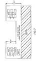
- FIG. 1 there is shown a top view of an ink jet print head according to the teachings of the present invention.
- the print head comprises an array of nozzles 1a-1d arranged in a line or a staggered configuration.
- Each nozzle is addressed by a logic AND gate (2a-2d) each of which contains logic circuitry and a heater driver transistor (not shown).
- the logic circuitry causes a respective driver transistor to turn on if a respective signal on a respective data input line (3a-3d) to the AND gate (2a-2d) and the respective enable clock lines (5a-5d), which is connected to the logic gate, are both logic ONE.
- signals on the enable clock lines (5a-5d) determine durations of the lengths of time current flows through the heaters in the particular nozzles 1a-1d.
- Data for driving the heater driver transistor may be provided from processed image data that is input to a data shift register 6.
- the latch register 7a-7d in response to a latch clock, receives the data from a respective shift register stage and provides a signal on the lines 3a-3d representative of the respective latched signal (logical ONE or ZERO) representing either that a dot is to be printed or not on a receiver.
- the lines A-A and B-B define the direction in which cross-sectional views are taken.
- Figures 1A and 1B show more detailed top views of the two types of heaters (the "notch type” and “split type” respectively) used in CIJ print heads. They produce asymmetric heating of the jet and thus cause ink jet deflection. Asymmetrical application of heat merely means supplying electrical current to one or the other section of the heater independently in the case of a split type heater. In the case of a notch type heater applied current to the notch type heater will inherently involve an asymmetrical heating of the ink. With reference now to Figure 1A there is illustrated a top view of an ink jet printhead nozzle with a notched type heater. The heater is formed adjacent the exit opening of the nozzle.
- the heater element material substantially encircles the nozzle bore but for a very small notched out area, just enough to cause an electrical open.
- one side of each heater is connected to a common bus line, which in turn is connected to the power supply typically +5 volts.
- the other side of each heater is connected to a logic AND gate within which resides an MOS transistor driver capable of delivering up to 30 mA of current to that heater.
- the AND gate has two logic inputs. One is from the Latch 7a-d which has captured the information from the respective shift register stage indicating whether the particular heater will be activated or not during the present line time.
- the other input is the enable clock that determines the length of time and sequence of pulses that are applied to the particular heater. Typically there are two or more enable clocks in the printhead so that neighboring heaters can be turned on at slightly different times to avoid thermal and other cross talk effects.
- FIG. 1B there is illustrated the nozzle with a split type heater wherein there are essentially two semicircular heater elements surrounding the nozzle bore adjacent the exit opening thereof. Separate conductors are provided to the upper and lower segments of each semi circle, it being understood that in this instance upper and lower refer to elements in the same plane. Vias are provided that electrically contact the conductors to metal layers associated with each of these conductors. These metal layers are in turn connected to driver circuitry formed on a silicon substrate as will be described below.
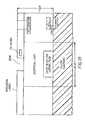
- FIG. 2 there is shown a simplified cross-sectional view of an operating nozzle across the B-B direction.
- an ink channel formed under the nozzle bores to supply the ink.
- This ink supply is under pressure typically between 15 to 25 psi for a bore diameter of about 8.8 micrometers.
- the ink in the delivery channel emanates from a pressurized reservoir (not shown), leaving the ink in the channel under pressure.
- the constant pressure can be achieved by employing an ink pressure regulator (not shown). Without any current flowing to the heater, a jet forms that is straight and flows directly into the gutter.
- On the surface of the printhead a symmetric meniscus forms around each nozzle that is a few microns larger in diameter than the bore.
- the meniscus in the heated side pulls in and the jet deflects away from the heater.
- the droplets that form then bypass the gutter and land on the receiver.
- the current through the heater is returned to zero, the meniscus becomes symmetric again and the jet direction is straight.
- the device could just as easily operate in the opposite way, that is, the deflected droplets are directed into the gutter and the printing is done on the receiver with the non-deflected droplets.
- having all the nozzles in a line is not absolutely necessary. It is just simpler to build a gutter that is essentially a straight edge rather than one that has a staggered edge that reflects the staggered nozzle arrangement.
- the heater resistance is of the order of 400 ohms
- the current amplitude is between 10 to 20 mA
- the pulse duration is about 2 microseconds
- the resulting deflection angle for pure water is of the order of a few degrees
- the application of periodic current pulses causes the jet to break up into synchronous droplets, to the applied pulses.
- These droplets form about 100 to 200 micrometers away from the surface of the printhead and for an 8.8 micrometers diameter bore and about 2 microseconds wide, 200 kHz pulse rate, they are typically 3 to 4 pL in size.
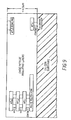
- the cross-sectional view taken along sectional line A-B and shown in Figure 3 represents an incomplete stage in the formation of a printhead in which nozzles are to be later formed in an array wherein CMOS circuitry is integrated on the same silicon substrate.
- CMOS circuitry is fabricated first on the silicon wafers.
- the CMOS process may be a standard 0.5 micrometers mixed signal process incorporating two levels of polysilicon and three levels of metal on a six inch diameter wafer. Wafer thickness is typically 675 micrometers.
- this process is represented by the three layers of metal, shown interconnected with vias. Also polysilicon level 2 and an N+ diffusion and contact to metal layer 1 are drawn to indicate active circuitry in the silicon substrate. Gates of CMOS transistors may be formed in the polysilicon layers.
- dielectric layers are deposited between them making the total thickness of the film on top of the silicon wafer about 4.5 micrometers.
- the structure illustrated in Figure 3 basically would provide the necessary transistors and logic gates for providing the control components illustrated in Figure 1 .
- CMOS fabrication steps a silicon substrate of approximately 675 micrometers in thickness and about 6 inches in diameter is provided. Larger or smaller diameter silicon wafers can be used equally as well.
- a plurality of transistors are formed in the silicon substrate through conventional steps of selectively depositing various materials to form these transistors as is well known.
- Supported on the silicon substrate are a series of layers eventually forming an oxide/nitride insulating layer that has one or more layers of polysilicon and metal layers formed therein in accordance with desired pattern. Vias are provided between various layers as needed and openings may be pre-provided in the surface for allowing access to metal layers to provide for bond pads.
- the various bond heads are provided to make respective connections of data, latch clock, enable clocks, and power provided from a circuit board mounted adjacent the printhead.
- the oxide/nitride insulating layers is about 4.5 micrometers in thickness.
- the structure illustrated in Figure 3 basically would provide the necessary interconnects, transistors and logic gates for providing the control components illustrated in Figure 1 .
- Figure 4 is a similar view to that of Figure 3 and also taken along line A-B a mask has been applied to the front side of the wafer and a window of 22 micrometers in diameter is defined. The dielectric layers in the window are then etched down to the silicon surface, which provides a natural etch stop as shown in Figure 4 .
- the first step is to fill in the window opened in the previous step with a sacrificial layer such as amorphous silicon or polyimide.
- the sacrificial layer is deposited in the recess formed between the front surface of the oxide/nitride insulating layer and the silicon substrate. These films are deposited at a temperature lower than 450 degrees centigrade to prevent melting of aluminum layers that are present.
- the wafer is then planarized.
- a thin, about 3500 angstroms, protection layer such as PECVD Si3N4, is deposited next and then the via3's to the metal three layer are opened.
- the vias can be filled with W and planarized, or they can be etched with sloped sidewalls so that the heater layer, which is deposited next can directly contact the metal3 layer.
- the heater layer consisting of about 50 angstroms of Ti and 600 angstroms of TiN is deposited and then patterned.
- a final thin protection (typically referred to as passivation) layer is deposited next. This layer must have properties that, as the one below the heater, protects the heater from the corrosive action of the ink, it must not be easily fouled by the ink and can be cleaned easily when fouled. It also provides protection against mechanical abrasion.
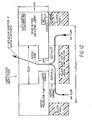
- FIG. 5 shows the cross-sectional view of the nozzle at this stage. It will be understood of course that along the silicon array many nozzle bores are simultaneously etched.
- the silicon wafer is then thinned from its initial thickness of 675 micrometers to 300 micrometers, see Figure 6A , a mask to open the ink channels is then applied to the backside of the wafer and the silicon is etched, in an STS etcher, all the way to the front surface of the silicon. Thereafter, the sacrificial layer is etched from the backside and the front side resulting in the finished device shown in Figure 6A .
- the device now has a flat top surface for easier cleaning and the bore is shallow enough for increased jet deflection.
- the temperature during post-processing was maintained below the 420 degrees centigrade annealing temperature of the heater, so its resistance remains constant for a long time.
- the embedded heater element effectively surrounds the nozzle bore and is proximate to the nozzle bore which reduces the temperature requirement of the heater for heating ink drops in the bore.
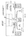
- Figure 6B there is illustrated a modified printhead structure wherein the bottom polysilicon layer is extended to the ink channel formed in the oxide layer to provide a polysilicon bottom heater element.
- the bottom heater element is used to provide an initial preheating of the ink as it enters the ink channel portion in the oxide layer.
- This modified structure is created during the CMOS process.
- the formation of the nozzle array is otherwise similar to that described for Figure 6A .
- the ink channel formed in the silicon substrate is illustrated as being a rectangular cavity passing centrally beneath the nozzle array.
- a long cavity in the center of the die tends to structurally weaken the printhead array so that if the array was subject to torsional stresses, such as during packaging, the membrane could crack.
- pressure variations in the ink channels due to low frequency pressure waves can cause jet jitter.
- the ink channel pattern defined in the back of the wafer therefore, is no longer a long rectangular recess running parallel to the direction of the row of nozzles but is instead a series of smaller rectangular cavities each feeding a single nozzle.
- each individual ink channel is fabricated to be a rectangle of twenty micrometers along the direction of the row of nozzles and 120 micrometers in the direction orthogonal to the row of nozzles, see Figure 8 .
- jet deflection could be further increased by increasing the portion of ink entering the bore of the nozzle with lateral rather than axial momentum. Such can be accomplished by blocking some of the fluid having axial momentum by building a block in the center of each nozzle array construct just below the nozzle bore.
- the same polysilicon layer that is used to form gates of the MOS transistors is used as the heater film.
- the dielectric film above the heater it is desirable to thin the dielectric film above the heater to about 0.35 micrometers.
- approximately 3.5 micrometers of the dielectric film is removed to form a nozzle bore region between the ink channel and a relatively wider and deep nozzle recess opening formed in the surface of the nozzle array.
- the nozzle recess is formed through an etch back process in a timed step.
- the final bore film thickness is approximately 1.0 micrometers.
- the silicon wafers are then thinned from their initial thickness of 675 micrometers to 300 micrometers.
- a mask to open channels is then applied to the backside of the wafers and the silicon is etched, in an STS etcher, all the way to the front surface of the silicon.
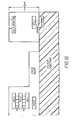
- the mask used is one that will leave behind a silicon bridge or rib between each nozzle of the nozzle array during the etching of the ink channel. These bridges extend all the way from the back of the silicon wafer to the front of the silicon wafer.
- the ink channel pattern defined in the back of the wafer therefore, is thus not a long rectangular recess running parallel to the direction of the row of nozzles but is instead a series of smaller rectangular cavities each feeding a single nozzle, see Figure 10 .
- jet stream deflection could be further increased by increasing the portion of ink entering the bore of the nozzle with lateral rather than axial momentum. Such can be accomplished by blocking some of the fluid having axial momentum by building a block in the center of each nozzle element just below the nozzle bore.
- FIG. 11 the cross-sectional view taken along sectional line A-A shows the lateral flow blocking structure and silicon ribs.
- a cross-sectional view taken along sectional line B-B is illustrated in Figure 12 .
- a phenomenon of the STS etcher called "footing.” Accordingly, when the silicon etch has reached the silicon/silicon dioxide interface, high speed lateral etching occurs because of charging of the oxide and deflection of the impinging reactive silicon etching ions laterally. This rapid lateral etch extends about 5 micrometers.
- the wafers are then placed in a conventional plasma etch chamber and the silicon in the center of the bore is etched anistropically about 5 micrometers down.
- Figures 11 and 12 show cross-sectional views of the resulting structure. Note that in Figure 12 , the cross-hatched area represents the silicon that has been removed to provide an access opening between a primary ink channel formed in the silicon substrate and the nozzle bore.
- a second method is one that does not depend on the footing effect. Instead, the silicon in the bore is etched isotropically from the front of the wafer for about 5 micrometers. The isotropic etch then removes the silicon laterally as well as vertically eventually removing the silicon shown in cross-section in Figure 13 thus facilitating fluidic contact between the ink channel and the bore. In this approach the blocking structure is shorter reflecting the etch back from the top fabrication method, which removes the cross-hatched region of silicon.
- the ink flowing into the bore is dominated by lateral momentum components, which is what is desired for increased droplet deflection.
- alignment of the ink channel openings in the back of the wafer to the nozzle array in the front of the wafer may be provided with an aligner system such as the Karl Suss aligner.
- Figure 14 there is provided a perspective view of the nozzle array with silicon based blocking structure showing the oxide/nitride layer partially removed to illustrate the blocking structure beneath the nozzle bore.
- the nozzle bore is spaced from the top of the blocking structure by an access opening.
- the blocking structure formed in the silicon substrate causes the ink which is under pressure in the ink cavity to flow about the blocking structure and to develop lateral momentum components.
- These lateral momentum components can be made unequal by the application of asymmetric heating and this then leads to stream deflection, as it is shown in Figures 12 and 13 .
- a method of constructing of a nozzle array with a ribbed structure but also featuring a lateral flow structure will now be described.
- Figure 3 which as noted above shows a cross-sectional view of the silicon wafer in the vicinity of the nozzle at the end of the CMOS fabrication sequence. It will be understood of course that although the description will be provided in the following paragraphs relative to formation of a single nozzle that the process is simultaneously applicable to a whole series of nozzles formed in a row along the wafer.
- the first step in the post-processing sequence is to apply a mask to the front of the wafer at the region of each nozzle opening to be formed.
- the mask is shaped so as to allow an etchant to open two 6 micrometer wide semicircular openings co-centric with the nozzle bore to be formed. The outside edges of these openings correspond to a 22 micrometers diameter circle.
- the dielectric layers in the semicircular regions are then etched completely to the silicon surface as shown in Figure 15 .
- a second mask is then applied and is of the shape to permit selective etching of the oxide block shown in Figure 16 .
- the oxide block is etched down to a final thickness or height from the silicon substrate of about 1.5 micrometers as shown in Figure 16 for a cross-section along sectional line B-B and in in Figure 17 for a cross-section along sectional line A-A.
- a cross-sectional view of the nozzle area along A-B is shown in Figure 18 .
- openings in the dielectric layer are filled with a sacrificial film such as amorphous silicon or polyimide and the wafers are planarized.
- a sacrificial film such as amorphous silicon or polyimide
- a thin layer of Ti/TiN is deposited next over the whole wafer followed by a much thicker W layer. The surface is then planarized in a chemical mechanical polishing process sequence that removes the W (wolfram) and Ti/TiN films from everywhere except from inside the via3's.
- the via3's can be etched with sloped sidewalls so that the heater layer, which is deposited next, can directly contact the metal3 layer.
- the heater layer consisting of about 50 angstroms of Ti and 600 angstroms of TiN is deposited and then patterned.
- a final thin protection (typically referred to as passivation) layer is deposited next.
- This layer must have properties that, as the one below the heater, protects the heater from the corrosive action of the ink, it must not be easily fouled by the ink and it can be cleaned easily when fouled. It also provides protection against mechanical abrasion and has the desired contact angle to the ink.
- the passivation layer may consist of a stack of films of different materials. The final film thickness encompassing the heater is about 1.5 micrometers.
- a bore mask is applied next to the front of the wafer and the passivation layers are etched to open the bore for each nozzle and the bond pads.
- Figures 19 and 20 show respective cross-sectional views of each nozzle at this stage. Although only one of the bond pads is shown it will be understood that multiple bond pads are formed in the nozzle array.
- the various bond pads are provided to make respective connections of data, latch clock, enable clocks, and power provided from a circuit board mounted adjacent the printhead or from a remote location.
- the silicon wafer is then thinned from its initial thickness of 675 micrometers to approximately 300 micrometers.
- a mask to open the ink channels is then applied to the backside of the wafer and the silicon is then etched in an STS deep silicon etch system, all the way to the front surface of the silicon.
- the sacrificial layer is etched from the backside and front side resulting in the finished device shown in Figures 21 , 24 and 25 .
- Alignment of the ink channel openings in the back of the wafer to the nozzle array in the front of the wafer may be provided with an aligner system such as the Karl Suss 1X aligner system.
- a polysilicon type heater can be incorporated in the bottom of the dielectric stack of each nozzle. These heaters also contribute to reducing the viscosity of the ink asymmetrically.
- ink flow passing through the access opening at the right side of the blocking structure will be heated while ink flow passing through the access opening at the left side of the blocking structure will not be heated.
- This asymmetric preheating of the ink flow tends to reduce the viscosity of ink having the lateral momentum components desired for deflection and because more ink will tend to flow where the viscosity is reduced there is a greater tendency for deflection of the ink in the desired direction; i.e. away from the heating elements adjacent the bore.
- the polysilicon type heating elements can-be of similar configuration to that of the primary heating elements adjacent the bore. Where heaters are used at both the top and the bottom of each nozzle bore, as illustrated in these Figures, the temperature at which each individual heater operates can be reduced dramatically. The reliability of the TiN heaters is much improved when they are allowed to operate at temperatures well below their annealing temperature.
- the lateral flow structure made using the oxide block allows the location of the oxide block to be aligned to within 0.02 micrometers relative to the nozzle bore.
- the ink flowing into the bore is dominated by lateral momentum components, which is what is desired for increased droplet deflection.
- etching of the silicon substrate was made to leave behind a silicon bridge or rib between each nozzle of the nozzle array during the etching of the ink channel.
- These bridges extend all the way from the back of the silicon wafer to the front of the silicon wafer.
- the ink channel pattern defined in the back of the wafer therefore, is a series of small rectangular cavities each feeding a single nozzle.
- the ink cavities may be considered to each comprise a primary ink channel formed in the silicon substrate and a secondary ink channel formed in the oxide/nitride layers with the primary and secondary ink channels communicating through an access opening established in the oxide/nitride layer.
- These access openings require ink to flow under pressure between the primary and secondary channels and develop lateral flow components because direct axial access to the secondary ink channel is effectively blocked by the oxide block.
- the secondary ink channel communicates with the nozzle bore.
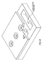
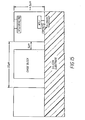
- the completed CMOS/MEMS print head 120 corresponding to any of the embodiments described herein is mounted on a supporting mount 110 having a pair of ink feed lines 130L, 130R connected adjacent end portions of the mount for feeding ink to ends of a longitudinally extending channel formed in the supporting mount.
- the channel faces the rear of the print head 120 and is thus in communication with the array of ink channels formed in the silicon substrate of the print head 120.
- the supporting mount which could be a ceramic substrate, includes mounting holes at the ends for attachment of this structure to a printer system.
Claims (9)
- Kontinuierlich arbeitender Tintenstrahldruckkopf (10a), bei dem Tinte während eines Druckvorgangs kontinuierlich in einer Ausstoßrichtung aus einer Reihe von Tintenstrahl-Düsenöffnungen (20) ausgestoßen wird, mit:einem Siliciumsubstrat mit darin ausgebildeten integrierten Schaltungen zum Steuern des Betriebs des Druckkopfs (10a), wobei das Siliciumsubstrat eine Reihe von entlang der Länge des Substrats darin ausgebildeten Tintenkanälen aufweist;einer Membrane, die aus einer elektrisch isolierenden Schicht bzw. elektrisch isolierenden Schichten besteht, welche das Siliciumsubstrat überlagert bzw. überlagern, wobei die Membrane die Reihe von Tintenstrahl-Düsenöffnungen (20) aufweist, die in der Membrane entlang der Länge des Siliciumsubstrats ausgebildet sind, wobei jede Düsenöffnung (20) mit einem jeweils anderen Tintenkanal in Verbindung steht und mit diesem ausgerichtet ist, und wobei der Querschnittsbereich eines jeden Tintenkanals in einer senkrecht zur Ausstoßrichtung verlaufenden Ebene größer ist als der Querschnittsbereich der entsprechenden Düsenöffnung (20) in einer senkrecht zur Ausstoßrichtung verlaufenden Ebene; undwobei die Tintenkanäle durch eine Reihe von Rippenstrukturen gebildet werden , die im Siliciumsubstrat ausgebildet sind, um eine entsprechende Rippenstruktur zwischen einander jeweils benachbarten Paaren von Tintenkanälen bereitzustellen, wobei die Rippenstrukturen quer zur Länge des Siliciumsubstrats verlaufen, um dem Substrat eine Festigkeit zu verleihen, und wobei die Dicke einer jeden Rippenstruktur der Gesamtdicke des Siliciumsubstrats entspricht, so dass die Rippenstrukturen in die Membrane eingreifen.
- Tintenstrahldruckkopf nach Anspruch 1, worin die Membrane eine Reihe vertikal voneinander getrennter Ebenen aus elektrisch leitfähigen Anschlüssen aufweist, wobei elektrisch leitfähige Verbindungsdurchgänge mindestens einige der Ebenen miteinander verbinden.
- Tintenstrahldruckkopf nach Anspruch 1 oder 2, worin der Druckkopf (10a) ein Heizelement aufweist, das einer jeden Düsenöffnung (20) benachbart angeordnet ist und derart wirkt, dass die Tinte an einer jeweiligen Düsenöffnung (20) asymmetrisch aufheizbar ist, was zu einer Umlenkung bestimmter Tintentropfen führt.
- Tintenstrahldruckkopf nach einem der Ansprüche 1 bis 3, worin die elektrisch isolierende Schicht bzw. die elektrisch isolierenden Schichten aus einem Oxid besteht bzw. bestehen.
- Tintenstrahldruckkopf nach einem der Ansprüche 1 bis 4, worin die integrierten Schaltungen CMOS Bauteile aufweisen.
- Tintenstrahldrucker nach Anspruch 1 oder 2, worin die Membrane, in der die Düsenöffnungen (20) jeweils ausgebildet sind, eine Passivierungsschicht aufweist, und worin ein Heizelement von der einer jeden Düsenöffnung (20) benachbarten Passivierungsschicht überlagert ist und derart wirkt, dass die Tinte an einer entsprechenden Düsenöffnung asymmetrisch aufgeheizt wird, was zu einer Umlenkung der Tintentropfen (11, 12) führt.
- Verfahren zum Betreiben eines kontinuierlich arbeitenden Tintenstrahldruckkopfs (10a) mit den Schritten:Bereitstellen von flüssiger, unter Druck stehender Tinte in einer Reihe von Tintenkanälen, die entlang der Länge eines Siliciumsubstrats derart ausgebildet sind, dass Tinte in einer Ausstoßrichtung ausgestoßen wird, wobei das Substrat eine darin ausgebildete Reihe integrierter Schaltungen zum Steuern des Betriebs des Druckkopfs umfasst; asymmetrisches Aufheizen der Tinte an jeder aus einer Vielzahl von Düsenöffnungen (20) zum Umlenken von Tintentropfen, wobei jede Düsenöffnung (20) mit einem entsprechenden Tintenkanal in Verbindung steht und mit diesem ausgerichtet ist, wobei der Querschnittsbereich eines entsprechenden Tintenkanals in einer senkrecht zur Ausstoßrichtung verlaufenden Ebene größer ist als der Querschnittsbereich einer entsprechenden Düsenöffnung (20) in einer senkrecht zur Ausstoßrichtung verlaufenden Ebene, und wobei die Düsenöffnung (20) in einer auf dem Substrat angeordneten Membrane ausgebildet und als eine sich in einer vorbestimmten Richtung erstreckende Anordnung angeordnet ist; und
worin jeder Tintenkanal durch Rippenstrukturen gebildet wird, die im Siliciumsubstrat ausgebildet sind, wobei eine entsprechende Rippenstruktur zwischen einander jeweils benachbarten Paaren von Tintenkanälen bereitgestellt wird, und worin die Rippenstrukturen quer zur Richtung der Anordnung der Düsenöffnungen (20) ausgerichtet sind und die Dicke einer jeden Rippenstruktur der Gesamtdicke des Siliciumsubstrats entspricht, so dass die Rippenstrukturen in die Membrane eingreifen. - Verfahren nach Anspruch 7, worin die integrierten Schaltungen CMOS Bauteile aufweisen, die zur Steuerung eines Heizelements verwendet werden, welches einer Düsenöffnung (20) benachbart ausgebildet ist.
- Verfahren nach Anspruch 8, worin eine elektrisch isolierende Schicht bzw. elektrisch isolierende Schichten auf dem Siliciumsubstrat gelagert ist bzw. sind und die elektrisch isolierende Schicht bzw. die elektrisch isolierenden Schichten eine Reihe vertikal getrennter Ebenen von elektrisch leitfähigen Anschlüssen und elektrisch leitfähigen Verbindungsdurchgängen aufweist bzw. aufweisen, die mindestens einige der Ebenen verbinden, und worin Signale von den im Substrat ausgebildeten CMOS Bauteilen durch die elektrisch leitfähigen Verbindungsdurchgänge übertragen werden.
Applications Claiming Priority (2)
| Application Number | Priority Date | Filing Date | Title |
|---|---|---|---|
| US751726 | 2000-12-29 | ||
| US09/751,726 US6474794B1 (en) | 2000-12-29 | 2000-12-29 | Incorporation of silicon bridges in the ink channels of CMOS/MEMS integrated ink jet print head and method of forming same |
Publications (2)
| Publication Number | Publication Date |
|---|---|
| EP1219422A1 EP1219422A1 (de) | 2002-07-03 |
| EP1219422B1 true EP1219422B1 (de) | 2008-05-21 |
Family
ID=25023218
Family Applications (1)
| Application Number | Title | Priority Date | Filing Date |
|---|---|---|---|
| EP01130219A Expired - Lifetime EP1219422B1 (de) | 2000-12-29 | 2001-12-19 | Einbauen von Silizium Brücken in Tintenkanäle eines Cmos/Mems integrierten Tintenstrahldruckkopfs und dazugehöriges Herstellungsverfahren |
Country Status (4)
| Country | Link |
|---|---|
| US (1) | US6474794B1 (de) |
| EP (1) | EP1219422B1 (de) |
| JP (1) | JP2002225275A (de) |
| DE (1) | DE60134112D1 (de) |
Families Citing this family (16)
| Publication number | Priority date | Publication date | Assignee | Title |
|---|---|---|---|---|
| US6450619B1 (en) * | 2001-02-22 | 2002-09-17 | Eastman Kodak Company | CMOS/MEMS integrated ink jet print head with heater elements formed during CMOS processing and method of forming same |
| US7052117B2 (en) | 2002-07-03 | 2006-05-30 | Dimatix, Inc. | Printhead having a thin pre-fired piezoelectric layer |
| US6746108B1 (en) | 2002-11-18 | 2004-06-08 | Eastman Kodak Company | Method and apparatus for printing ink droplets that strike print media substantially perpendicularly |
| US6821450B2 (en) * | 2003-01-21 | 2004-11-23 | Hewlett-Packard Development Company, L.P. | Substrate and method of forming substrate for fluid ejection device |
| US7281778B2 (en) | 2004-03-15 | 2007-10-16 | Fujifilm Dimatix, Inc. | High frequency droplet ejection device and method |
| US8491076B2 (en) | 2004-03-15 | 2013-07-23 | Fujifilm Dimatix, Inc. | Fluid droplet ejection devices and methods |
| WO2006074016A2 (en) | 2004-12-30 | 2006-07-13 | Fujifilm Dimatix, Inc. | Ink jet printing |
| US7364276B2 (en) * | 2005-09-16 | 2008-04-29 | Eastman Kodak Company | Continuous ink jet apparatus with integrated drop action devices and control circuitry |
| US7249830B2 (en) * | 2005-09-16 | 2007-07-31 | Eastman Kodak Company | Ink jet break-off length controlled dynamically by individual jet stimulation |
| US7434919B2 (en) * | 2005-09-16 | 2008-10-14 | Eastman Kodak Company | Ink jet break-off length measurement apparatus and method |
| US7673976B2 (en) * | 2005-09-16 | 2010-03-09 | Eastman Kodak Company | Continuous ink jet apparatus and method using a plurality of break-off times |
| US7777395B2 (en) * | 2006-10-12 | 2010-08-17 | Eastman Kodak Company | Continuous drop emitter with reduced stimulation crosstalk |
| US7988247B2 (en) | 2007-01-11 | 2011-08-02 | Fujifilm Dimatix, Inc. | Ejection of drops having variable drop size from an ink jet printer |
| US8733902B2 (en) * | 2008-05-06 | 2014-05-27 | Hewlett-Packard Development Company, L.P. | Printhead feed slot ribs |
| CN102470673A (zh) * | 2009-07-31 | 2012-05-23 | 惠普开发有限公司 | 采用中心墨水供给通道的喷墨打印头和方法 |
| US8632162B2 (en) | 2012-04-24 | 2014-01-21 | Eastman Kodak Company | Nozzle plate including permanently bonded fluid channel |
Family Cites Families (16)
| Publication number | Priority date | Publication date | Assignee | Title |
|---|---|---|---|---|
| US1941001A (en) | 1929-01-19 | 1933-12-26 | Rca Corp | Recorder |
| US3373437A (en) | 1964-03-25 | 1968-03-12 | Richard G. Sweet | Fluid droplet recorder with a plurality of jets |
| GB1143079A (en) | 1965-10-08 | 1969-02-19 | Hertz Carl H | Improvements in or relating to recording devices for converting electrical signals |
| US3946398A (en) | 1970-06-29 | 1976-03-23 | Silonics, Inc. | Method and apparatus for recording with writing fluids and drop projection means therefor |
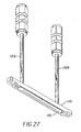
| CA1127227A (en) | 1977-10-03 | 1982-07-06 | Ichiro Endo | Liquid jet recording process and apparatus therefor |
| CA1158706A (en) | 1979-12-07 | 1983-12-13 | Carl H. Hertz | Method and apparatus for controlling the electric charge on droplets and ink jet recorder incorporating the same |
| US4552974A (en) | 1982-12-07 | 1985-11-12 | Asahi Kasei Kogyo Kabushiki Kaisha | Process for producing diphenylmethane dicarbamates |
| US4894664A (en) | 1986-04-28 | 1990-01-16 | Hewlett-Packard Company | Monolithic thermal ink jet printhead with integral nozzle and ink feed |
| US4875968A (en) * | 1989-02-02 | 1989-10-24 | Xerox Corporation | Method of fabricating ink jet printheads |
| AU657930B2 (en) * | 1991-01-30 | 1995-03-30 | Canon Kabushiki Kaisha | Nozzle structures for bubblejet print devices |
| US5880759A (en) | 1995-04-12 | 1999-03-09 | Eastman Kodak Company | Liquid ink printing apparatus and system |
| US5825385A (en) | 1995-04-12 | 1998-10-20 | Eastman Kodak Company | Constructions and manufacturing processes for thermally activated print heads |
| US6000787A (en) * | 1996-02-07 | 1999-12-14 | Hewlett-Packard Company | Solid state ink jet print head |
| US5812159A (en) | 1996-07-22 | 1998-09-22 | Eastman Kodak Company | Ink printing apparatus with improved heater |
| US5966154A (en) * | 1997-10-17 | 1999-10-12 | Eastman Kodak Company | Graphic arts printing plate production by a continuous jet drop printing with asymmetric heating drop deflection |
| US6079821A (en) | 1997-10-17 | 2000-06-27 | Eastman Kodak Company | Continuous ink jet printer with asymmetric heating drop deflection |
-
2000
- 2000-12-29 US US09/751,726 patent/US6474794B1/en not_active Expired - Lifetime
-
2001
- 2001-12-19 EP EP01130219A patent/EP1219422B1/de not_active Expired - Lifetime
- 2001-12-19 DE DE60134112T patent/DE60134112D1/de not_active Expired - Lifetime
- 2001-12-20 JP JP2001387253A patent/JP2002225275A/ja active Pending
Also Published As
| Publication number | Publication date |
|---|---|
| DE60134112D1 (de) | 2008-07-03 |
| US6474794B1 (en) | 2002-11-05 |
| JP2002225275A (ja) | 2002-08-14 |
| EP1219422A1 (de) | 2002-07-03 |
Similar Documents
| Publication | Publication Date | Title |
|---|---|---|
| US6943037B2 (en) | CMOS/MEMS integrated ink jet print head and method of forming same | |
| US6450619B1 (en) | CMOS/MEMS integrated ink jet print head with heater elements formed during CMOS processing and method of forming same | |
| US6382782B1 (en) | CMOS/MEMS integrated ink jet print head with oxide based lateral flow nozzle architecture and method of forming same | |
| EP1234668B1 (de) | Cmos/mems-integrierter Tintenstrahldruckkopf mit länglicher Bohrung und Verfahren zu seiner Herstellung | |
| US6439703B1 (en) | CMOS/MEMS integrated ink jet print head with silicon based lateral flow nozzle architecture and method of forming same | |
| US6491376B2 (en) | Continuous ink jet printhead with thin membrane nozzle plate | |
| EP1219422B1 (de) | Einbauen von Silizium Brücken in Tintenkanäle eines Cmos/Mems integrierten Tintenstrahldruckkopfs und dazugehöriges Herstellungsverfahren | |
| EP1219427B1 (de) | Einarbeitung von Zusatzheizelementen in die Tintenkanäle von einem Cmos/mems integrierten Tintenstrahldruckkopf und Verfahren zu deren Herstellung | |
| US6663221B2 (en) | Page wide ink jet printing | |
| US20090033727A1 (en) | Lateral flow device printhead with internal gutter | |
| EP1219426B1 (de) | Cmos/mems integrierter Tintenstrahldruckkopf und Verfahren zu seiner Herstellung | |
| EP1219424B1 (de) | Cmos/mems integrierter Tintenstrahldruckkopf mit Querflussdüsenarchitektur auf Siliziumbasis und Verfahren zu seiner Herstellung | |
| US20090295861A1 (en) | Continuous fluid jet ejector with anisotropically etched fluid chambers |
Legal Events
| Date | Code | Title | Description |
|---|---|---|---|
| PUAI | Public reference made under article 153(3) epc to a published international application that has entered the european phase |
Free format text: ORIGINAL CODE: 0009012 |
|
| AK | Designated contracting states |
Kind code of ref document: A1 Designated state(s): AT BE CH CY DE DK ES FI FR GB GR IE IT LI LU MC NL PT SE TR |
|
| AX | Request for extension of the european patent |
Free format text: AL;LT;LV;MK;RO;SI |
|
| 17P | Request for examination filed |
Effective date: 20021212 |
|
| AKX | Designation fees paid |
Designated state(s): DE FR GB |
|
| 17Q | First examination report despatched |
Effective date: 20050902 |
|
| GRAP | Despatch of communication of intention to grant a patent |
Free format text: ORIGINAL CODE: EPIDOSNIGR1 |
|
| GRAS | Grant fee paid |
Free format text: ORIGINAL CODE: EPIDOSNIGR3 |
|
| GRAA | (expected) grant |
Free format text: ORIGINAL CODE: 0009210 |
|
| AK | Designated contracting states |
Kind code of ref document: B1 Designated state(s): DE FR GB |
|
| REG | Reference to a national code |
Ref country code: GB Ref legal event code: FG4D |
|
| REF | Corresponds to: |
Ref document number: 60134112 Country of ref document: DE Date of ref document: 20080703 Kind code of ref document: P |
|
| PLBE | No opposition filed within time limit |
Free format text: ORIGINAL CODE: 0009261 |
|
| STAA | Information on the status of an ep patent application or granted ep patent |
Free format text: STATUS: NO OPPOSITION FILED WITHIN TIME LIMIT |
|
| 26N | No opposition filed |
Effective date: 20090224 |
|
| PGFP | Annual fee paid to national office [announced via postgrant information from national office to epo] |
Ref country code: GB Payment date: 20131126 Year of fee payment: 13 |
|
| PGFP | Annual fee paid to national office [announced via postgrant information from national office to epo] |
Ref country code: FR Payment date: 20131126 Year of fee payment: 13 |
|
| PGFP | Annual fee paid to national office [announced via postgrant information from national office to epo] |
Ref country code: DE Payment date: 20141222 Year of fee payment: 14 |
|
| GBPC | Gb: european patent ceased through non-payment of renewal fee |
Effective date: 20141219 |
|
| REG | Reference to a national code |
Ref country code: FR Ref legal event code: ST Effective date: 20150831 |
|
| PG25 | Lapsed in a contracting state [announced via postgrant information from national office to epo] |
Ref country code: GB Free format text: LAPSE BECAUSE OF NON-PAYMENT OF DUE FEES Effective date: 20141219 |
|
| PG25 | Lapsed in a contracting state [announced via postgrant information from national office to epo] |
Ref country code: FR Free format text: LAPSE BECAUSE OF NON-PAYMENT OF DUE FEES Effective date: 20141231 |
|
| REG | Reference to a national code |
Ref country code: DE Ref legal event code: R119 Ref document number: 60134112 Country of ref document: DE |
|
| PG25 | Lapsed in a contracting state [announced via postgrant information from national office to epo] |
Ref country code: DE Free format text: LAPSE BECAUSE OF NON-PAYMENT OF DUE FEES Effective date: 20160701 |