EP1217629A1 - Procédé d'acquisition par échantillonnage de signaux analogiques et système d'acquisition pour la mise en oeuvre de ce procédé - Google Patents
Procédé d'acquisition par échantillonnage de signaux analogiques et système d'acquisition pour la mise en oeuvre de ce procédé Download PDFInfo
- Publication number
- EP1217629A1 EP1217629A1 EP01403322A EP01403322A EP1217629A1 EP 1217629 A1 EP1217629 A1 EP 1217629A1 EP 01403322 A EP01403322 A EP 01403322A EP 01403322 A EP01403322 A EP 01403322A EP 1217629 A1 EP1217629 A1 EP 1217629A1
- Authority
- EP
- European Patent Office
- Prior art keywords
- signal
- bus
- memory
- analog signal
- write
- Prior art date
- Legal status (The legal status is an assumption and is not a legal conclusion. Google has not performed a legal analysis and makes no representation as to the accuracy of the status listed.)
- Granted
Links
- 238000005070 sampling Methods 0.000 title claims abstract description 27
- 238000000034 method Methods 0.000 title claims abstract description 15
- 239000011159 matrix material Substances 0.000 claims abstract description 16
- 239000003990 capacitor Substances 0.000 claims description 19
- 230000004913 activation Effects 0.000 claims description 3
- 238000004364 calculation method Methods 0.000 claims description 3
- 230000003111 delayed effect Effects 0.000 claims description 2
- 230000007547 defect Effects 0.000 description 3
- 238000005516 engineering process Methods 0.000 description 2
- 230000014759 maintenance of location Effects 0.000 description 2
- 230000035945 sensitivity Effects 0.000 description 2
- 238000003491 array Methods 0.000 description 1
- 230000015556 catabolic process Effects 0.000 description 1
- 230000020411 cell activation Effects 0.000 description 1
- 210000001520 comb Anatomy 0.000 description 1
- 230000008878 coupling Effects 0.000 description 1
- 238000010168 coupling process Methods 0.000 description 1
- 238000005859 coupling reaction Methods 0.000 description 1
- 238000006731 degradation reaction Methods 0.000 description 1
- 230000001934 delay Effects 0.000 description 1
- 230000009977 dual effect Effects 0.000 description 1
- 230000000694 effects Effects 0.000 description 1
- 230000000873 masking effect Effects 0.000 description 1
- 239000002184 metal Substances 0.000 description 1
- 230000003071 parasitic effect Effects 0.000 description 1
- 239000000758 substrate Substances 0.000 description 1
- 238000011144 upstream manufacturing Methods 0.000 description 1
Images
Classifications
-
- G—PHYSICS
- G11—INFORMATION STORAGE
- G11C—STATIC STORES
- G11C8/00—Arrangements for selecting an address in a digital store
- G11C8/04—Arrangements for selecting an address in a digital store using a sequential addressing device, e.g. shift register, counter
-
- G—PHYSICS
- G11—INFORMATION STORAGE
- G11C—STATIC STORES
- G11C27/00—Electric analogue stores, e.g. for storing instantaneous values
- G11C27/02—Sample-and-hold arrangements
-
- G—PHYSICS
- G11—INFORMATION STORAGE
- G11C—STATIC STORES
- G11C27/00—Electric analogue stores, e.g. for storing instantaneous values
- G11C27/02—Sample-and-hold arrangements
- G11C27/024—Sample-and-hold arrangements using a capacitive memory element
Definitions
- the invention relates to a method of acquisition by sampling of analog signals, of the type including the operations of sampling a signal high speed analog, store samples in a matrix of memory cells and re-read the low speed cells and an acquisition system for the implementation of this process.
- the object of the present invention is to provide a system for acquiring an analog signal by sampling, which eliminates the drawbacks above.
- the acquisition process according to the invention is characterized in that provision is made in each memory cell two memory devices identical, stores in a memory device a analog signal sample and in the other one sample of this signal but taken substantially into phase opposition.
- the signal in phase opposition to the phase signal is delayed before its application to the write bus channel corresponding, with a predetermined duration of time, advantageously equal to half a signal period sampling.
- the analog signal acquisition system by sampling, of the type comprising an array of analog memory cells arranged in a plurality of rows and columns, each cell being connected to a write bus and a read bus and with two control signal inputs activation, obtained from a clock signal, a horizontal shift register and a vertical register, for applying control signals to cells activation for write and read operations cells, is characterized in that the write bus and the read bus each have two channels, which one of the two write bus channels receives the signal analog to be sampled substantially in opposition to phase with respect to the other channel and in that each memory cell has two memory devices each connected to one of the two channels of the write bus and the bus of reading.
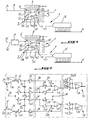
- FIG. 1 shows schematically that a system acquisition of analog signals, by sampling according to the invention comes from a combination of two sampling structures each with a matrix of cells analog memory 1, 2 arranged in rows and columns of which only one cell is shown in 3, 3 '.
- Each cell is connected, in a manner known per se, to a write bus 4 and read bus 5 connected respectively to an input circuit 6 and a outlet 7, for matrix 1, and 4 ', 5', 6 ', 7' for matrix 2.
- each cell can be activated for writing a sample of the analog signal and reading this sample by two control signals from a register at horizontal offset 8, 8 'and a vertical register 9, 9 '.
- the output circuit includes a converter analog-digital 12, 12 'intended to convert analog information read in a digital value, available at output terminal 14, 14 '.
- a converter analog-digital 12, 12 'intended to convert analog information read in a digital value available at output terminal 14, 14 '.
- At the terminals input 15, 15 'of the input circuits 6, 6' of the two matrices 1 and 2 are applied, respectively, the signal analog to sample and the same signal but in phase opposition.
- each cell represented memory 3 of the matrix 1 comprises essentially a flying capacitor Cs for storing samples with two write circuits switches S1 and S2 connected by an electrode write bus 5 and return bus respectively constituting the reference bus 20, the capacitor Cs being mounted between the other two electrodes of the switches.
- the reading circuit of the capacitor Cs is also mounted between two read switches S3 and S4.
- a terminal of switch S3 is connected to the interconnection between the storage capacitor Cs and switch S1, while the other electrode is connected to the output of a sense amplifier 21 which is connected to a terminal of the analog converter digital 12.
- switch S4 an electrode is connected to the interconnection between the capacitor CS and switch S2.
- the other electrode is connected to a input of the sense amplifier 21, the other input of this being connected to the reference potential 20.
- the FIG. 1 also illustrates an AND gate 22 shown as example of the switch S1 control. The figure again schematically shows that at the two entrances of the AND gate 22 are applied respectively a signal of command from horizontal register 8 and a control signal produced by the vertical register 9.
- the memory cell 3 ′ of the matrix 2 comprises, from analogous to cell 3 of matrix 1 a storage capacitor Cs' including the write circuit includes switches S1 'and S2' and the circuit read switches S3 'and S4'. AND gates and matrix 2 amplifier are designated by the references 22 'and 21'.
- FIG 1 the acquisition system according to the invention, which without the delay element 17 has a purely differential structure obtained by the association of two distinct networks connected in differential, is shown in Figure 2, in what concerns the structures of memory cells, in the form of a differential cell.
- the structure allowing to access these elementary cells both in writing that on reading consists of a shift register horizontal of for example 128 scales used in write and read and a right vertical register of 20 scales as well as a left register of 20 others flip-flops.
- the right register is used in the process of reading multiplexing.
- Left and right registers can also be used in the subsampling process by mask, i.e. by masking the write pointer, needed to reduce frequency writing.
- Write and read operations are clocked by a clock signal produced by a clock device not shown.
- the matrix is traversed by the column pointer, starting with the left column.
- the column pointer is shifted by one notch in the horizontal register in order to point to the second column etc, up to the last column.
- the first rocker of the register is therefore positioned in logical state 1 and all the others at 0.
- the pointer In each column, the pointer is moved vertically within a DLL type circuit. This circuit provides sub-multiple delays of the system clock period, here for example 1/20.
- the vertical pointer circulating in the DLL must be of a calibrated duration less than the clock period of the system. For a cell to be written, it is necessary, as it was indicated above, that it is located the intersection of an active row and column. Yes the vertical pointer is 17ns in length, so at a instant 17 cells are active and each ns the pointer has moved one cell in the direction vertical, hence the frequency of writing an ns for a system clock at 50 MHz in this example.
- this device calls on an automaton which sequences all operations, namely the management of pointer registers and control of the various switches. This technique is known per se and therefore does not need to be described in more detail.
- the dual differential memory cell flying capacitors includes, in addition to this which is shown in figure 1, two amplifiers writing followers 24, 24 ', which are mounted upstream of the switches S1 and S1 '.
- the two Figure 1 elementary memory cells are now connected to the same reference 20.
- a SO switch which optimizes bandwidth of the cell according to the size of the switches S2, S2 'and SO, advantageously formed by switch transistors.
- the sense amplifiers 21, 21 ' are located inside the device for reading a line and are connected to the read switches S3, S4 and S3 ', S4' via switches respectively S5, S6, S7 and S5 ', S6' and S7 '.
- the negative input of amplifier 21 is connected to switch S3 by means of switch S5 and at switch S4 by means of switch S6.
- the entrance positive is connected to switch S4 by via the switch S7. This description applies analogously to the amplifier 21 '.
- the multiplexing device has two output amplifiers 26, 26 'and twenty switches multiplexing input connected in parallel Sm0 to Sm19 and Sm0 'to Sm19', which can be linked selectively at the output of the output amplifier 21, 21 ' correspondent of the line reading device.
- the switches having the same indices receive the same logical command. So the switches S1 and S1 'are controlled simultaneously.
- the switch So receives the same command as switch S2 and S2 '.
- the input signal to be sampled is applied to the terminal 15 and in phase opposition to the input terminal 15 '. It is reread on outputs 14 and 14 '.
- the signal from reference 20 could be ground.
- the sampling write sequence of the signal applied as input is carried out by the switches S1 and S2.
- switches S3 and S4 remain open and switches S5 and S7 closed.
- S1 switches and S2 are simultaneously closed at the start of sampling. They remain closed during the whole sampling phase. The end of sampling is achieved by opening the switch first S2, followed by that of switch S1 a few nanoseconds later.
- the line reading system is reset to zero on each reading.
- the three switches S5, S6, S7 are used for reset zero of the amplifier 21.
- switches S5 and S7 are closed.
- the amplifier 21 is configured as a follower via a switch S5.
- S7 switch allows load flow residuals stored on the part of bus 29 towards the reference. After resetting the reading of each cell can take place.
- Switches S5 and S7 are open at the end of the reset phase and switch S6 is closed.
- S3 and S4 switches are closed in order to connect the capacitor Cs in feedback on amplifier 21.
- Reading is carried out line by line in order to scan the entire matrix.
- the switches multiplexing are therefore closed in turn in order to successively select all the lines.
- the different cells to know the 128 cells in the example, are successively selected using switches above and the reset sequence and the reading will be repeated as many times as necessary.
- the method according to the invention if it provides for a delay in channel 6 'of the opposing input signal phase to signal in channel 6 requires a reading algorithm modified with respect to a structure purely differential without delay. Indeed, if the delay is chosen equal to half a frequency period sampling there are now twice as many samples to scan and removing mode common is no longer achievable with an amplifier differential. It must be done by calculation after scanning.
- the time difference brought by the element delay 17 is equivalent to a system in which both sampling combs are interlaced by half a period, that the delay for the interval sampling is halved. We thus obtain doubling the effective sampling frequency of the constituted system.
- ECH (2i - 1) ES (i) - ESI (i) + MS
- ECH (2i) ES (i + 1) - ESI (i) + MS
- ECH (i) is the sample of rank i
- ES (i) is the sample of rank i from the half-matrix which processes the non-inverted signal
- ESI (i + 1) is the sample of rank i +1 from the half-matrix which processes the inverted signal
- MS is the mid-scale of analog-digital converters, which is equal to 2 11 for analog-digital converters with twelve binary digits.
- the invention effectively eliminates the common mode. We see that the sum of the samples shifted by an index, filters the reconstructed signal.
- switches S1 and S1 ' are in CMOS technology, while switches S2 to S7 and S2 'to S7' are in NMOS technology.
- the present invention by proposing a structure of differential cells removes defects from single cells with flying capacitor, which reside in the high sensitivity of the system to substrate noise, in particular capacitors formed by transistors MOS with metal tracks, in signal pollution recorded by the effect called "dropout" and in a relatively low signal to noise ratio.
- flying capacitor which reside in the high sensitivity of the system to substrate noise, in particular capacitors formed by transistors MOS with metal tracks, in signal pollution recorded by the effect called "dropout" and in a relatively low signal to noise ratio.
- charges stored in capacitors memory slowly escape via leaks switches hence an error which increases with duration retention. However, this retention is not the same for the first cells read only for the last. This defect is therefore difficult to compensate by calculation.
- the signal to noise ratio is limited by induced noise by parasitic capacitive couplings with signals digital.
- the low value of the memory capacitor dictated by the bandwidth sought leads to a not insignificant sensitivity to coupled noise.
- the invention provides to duplicate the whole matrix in order to constitute a differential system to process two signals in phase opposition. In this way, the distortions will be seen as common mode and eliminates by rejection of common mode of the reading device. Moreover, the maximum amplitude of the accessible signal is doubled, from does differential mode, compared to a solution simple. So even without any common mode rejection, the signal to noise ratio has already been improved by 6 dB. The rejection of the common mode is all the more effective vis-à-vis spurious signals that the two structures are symmetrical. To this end, the achievement of the matrix with elementary memory cells differential is particularly advantageous.
Landscapes
- Engineering & Computer Science (AREA)
- Microelectronics & Electronic Packaging (AREA)
- Electronic Switches (AREA)
- Measurement Of Current Or Voltage (AREA)
- Inspection Of Paper Currency And Valuable Securities (AREA)
- Color Television Image Signal Generators (AREA)
- Dram (AREA)
- Transforming Light Signals Into Electric Signals (AREA)
Abstract
Description
- La figure 1 montre schématiquement un système d'acquisition d'un signal analogique par échantillonnage, selon l'invention, comportant deux matrices mémoire ; et
- La figure 2 montre schématiquement la structure d'une cellule mémoire selon la présente invention ;
Claims (11)
- Procédé d'acquisition par échantillonnage de signaux analogiques, du type comprenant les opérations d'échantillonner un signal analogique, à grande vitesse, stocker les échantillons dans une matrice de cellules mémoires et de relire les cellules à faible vitesse, caractérisé en ce que l'on prévoit dans chaque cellule mémoire deux dispositifs mémoires identiques, stocke dans un dispositif mémoire un échantillon du signal analogique et dans l'autre un échantillon de ce signal pris sensiblement en opposition de phase.
- Procédé selon la revendication 2, caractérisé en ce qu'un des signaux est retardé d'une durée avantageusement égale à une demi-période du signal d'échantillonnage, avant l'application au dispositif mémoire.
- Système d'acquisition d'un signal analogique par échantillonnage, du type comportant une matrice de cellules mémoires analogiques agencées en une pluralité de lignes et de colonnes, chaque cellule étant reliée à un bus d'écriture et un bus de lecture et comporte deux entrées de signaux de commande d'activation, obtenu à partir d'un signal d'horloge, un registre à décalage horizontal et un registre vertical destinés à appliquer aux cellules des signaux de commande d'activation pour les opérations d'écriture et de lecture des cellules, caractérisé en ce que le bus d'écriture et le bus de lecture comportent chacun deux canaux (4, 4' ; 5, 5'), que l'un (4') des deux canaux du bus d'écriture reçoit le signal analogique à échantillonner en opposition de phase par rapport à l'autre canal (4) et en ce que chaque cellule mémoire (3) comporte deux dispositifs mémoires chacun relié à l'un des deux canaux (4, 4') du bus d'écriture et du bus de lecture (5, 5').
- Système selon la revendication 3, caractérisé en ce qu'il présente une structure différentielle, comportant deux entrées (15, 15') recevant respectivement le signal analogique à échantillonner et le signal analogique à échantillonner en opposition de phase.
- Système selon la revendication 4, caractérisé en ce que le circuit d'entrée (6') de l'un (4') des deux canaux de bus d'écriture comporte un élément à retard (17), avantageusement d'une durée correspondante à une demi-période de la fréquence d'échantillonnage.
- Système selon l'une des revendications 3 à 5, caractérisé en ce que chaque dispositif mémoire d'une cellule mémoire comporte un condensateur de stockage (Cs, Cs'), monté flottant dans un circuit d'écriture entre le bus d'écriture (4, 4') et un potentiel de références (20, 20') et un circuit de lecture entre le bus de lecture (5, 5') et ledit potentiel de référence, les deux circuits comportant des interrupteurs susceptibles d'être commandés sélectivement.
- Système selon la revendication 6, caractérisé en ce que le condensateur de stockage (Cs, Cs') est disposé dans le circuit d'écriture entre deux interrupteurs (S1, S1' ; S2, S2').
- Système selon l'une des revendications 5 ou 6 caractérisé en ce que le condensateur de stockage (Cs, Cs') est monté dans le circuit de lecture entre deux interrupteurs (S3, S3' ; S4, S4').
- Système selon l'une des revendications 6 à 8, caractérisé en ce qu'une cellule mémoire est réalisée sous forme d'une cellule différentielle, dans laquelle le potentiel de référence (20) est commun aux deux dispositifs mémoires.
- Système selon la revendication 8, caractérisé en ce que les deux condensateurs de stockage (Cs ; Cs') sont reliés par un interrupteur optionnel (SO) d'élargissement de la bande passante de la cellule.
- Système selon l'une des revendications 4 à 10, caractérisé en ce qu'il comporte un dispositif de reconstitution du signal échantillonné par calcul après numérisation.
Applications Claiming Priority (2)
| Application Number | Priority Date | Filing Date | Title |
|---|---|---|---|
| FR0016678 | 2000-12-20 | ||
| FR0016678A FR2818423B1 (fr) | 2000-12-20 | 2000-12-20 | Procede d'acquisition par echantillonage de signaux analogiques et systeme d'acquisition pour la mise en oeuvre de ce procede |
Publications (2)
| Publication Number | Publication Date |
|---|---|
| EP1217629A1 true EP1217629A1 (fr) | 2002-06-26 |
| EP1217629B1 EP1217629B1 (fr) | 2007-07-25 |
Family
ID=8857935
Family Applications (1)
| Application Number | Title | Priority Date | Filing Date |
|---|---|---|---|
| EP01403322A Expired - Lifetime EP1217629B1 (fr) | 2000-12-20 | 2001-12-20 | Procédé d'acquisition par échantillonnage de signaux analogiques et système d'acquisition pour la mise en oeuvre de ce procédé |
Country Status (5)
| Country | Link |
|---|---|
| US (1) | US6667894B2 (fr) |
| EP (1) | EP1217629B1 (fr) |
| AT (1) | ATE368287T1 (fr) |
| DE (1) | DE60129527T2 (fr) |
| FR (1) | FR2818423B1 (fr) |
Families Citing this family (2)
| Publication number | Priority date | Publication date | Assignee | Title |
|---|---|---|---|---|
| US7198197B2 (en) * | 2002-11-05 | 2007-04-03 | Rambus, Inc. | Method and apparatus for data acquisition |
| US10163521B2 (en) * | 2016-10-11 | 2018-12-25 | Microchip Technology Incorporated | High voltage bootstrap sampling circuit |
Citations (3)
| Publication number | Priority date | Publication date | Assignee | Title |
|---|---|---|---|---|
| US4271488A (en) * | 1979-04-13 | 1981-06-02 | Tektronix, Inc. | High-speed acquisition system employing an analog memory matrix |
| US5526286A (en) * | 1994-02-16 | 1996-06-11 | Tektronix, Inc. | Oversampled logic analyzer |
| JPH11283394A (ja) * | 1998-03-30 | 1999-10-15 | Rohm Co Ltd | サンプルホールド回路及びリニアコーディック回路 |
Family Cites Families (4)
| Publication number | Priority date | Publication date | Assignee | Title |
|---|---|---|---|---|
| US5526301A (en) * | 1995-01-13 | 1996-06-11 | Tektronix, Inc. | High-speed analog acquisition including signal processing |
| DE69520673T2 (de) * | 1995-09-27 | 2001-08-02 | Stmicroelectronics S.R.L., Agrate Brianza | Analogspeicher zur Speicherung eines Bildes QCIF oder ähnliche als elektrische ladung |
| JPH11283396A (ja) | 1998-03-27 | 1999-10-15 | Sony Corp | メモリ装置 |
| US6091619A (en) * | 1999-04-23 | 2000-07-18 | Tektronix, Inc. | Array architecture for long record length fast-in slow-out (FISO) analog memory |
-
2000
- 2000-12-20 FR FR0016678A patent/FR2818423B1/fr not_active Expired - Fee Related
-
2001
- 2001-12-20 EP EP01403322A patent/EP1217629B1/fr not_active Expired - Lifetime
- 2001-12-20 US US10/022,839 patent/US6667894B2/en not_active Expired - Fee Related
- 2001-12-20 AT AT01403322T patent/ATE368287T1/de not_active IP Right Cessation
- 2001-12-20 DE DE60129527T patent/DE60129527T2/de not_active Expired - Lifetime
Patent Citations (3)
| Publication number | Priority date | Publication date | Assignee | Title |
|---|---|---|---|---|
| US4271488A (en) * | 1979-04-13 | 1981-06-02 | Tektronix, Inc. | High-speed acquisition system employing an analog memory matrix |
| US5526286A (en) * | 1994-02-16 | 1996-06-11 | Tektronix, Inc. | Oversampled logic analyzer |
| JPH11283394A (ja) * | 1998-03-30 | 1999-10-15 | Rohm Co Ltd | サンプルホールド回路及びリニアコーディック回路 |
Non-Patent Citations (1)
| Title |
|---|
| PATENT ABSTRACTS OF JAPAN vol. 2000, no. 01 31 January 2000 (2000-01-31) * |
Also Published As
| Publication number | Publication date |
|---|---|
| ATE368287T1 (de) | 2007-08-15 |
| FR2818423B1 (fr) | 2003-04-04 |
| US6667894B2 (en) | 2003-12-23 |
| DE60129527D1 (de) | 2007-09-06 |
| FR2818423A1 (fr) | 2002-06-21 |
| US20030012057A1 (en) | 2003-01-16 |
| DE60129527T2 (de) | 2008-04-17 |
| EP1217629B1 (fr) | 2007-07-25 |
Similar Documents
| Publication | Publication Date | Title |
|---|---|---|
| EP0367650B1 (fr) | Dispositif photosensible du type à amplification du signal au niveau des points photosensibles | |
| EP1646147B1 (fr) | Filtre analogique à composants passifs pour signaux à temps discret | |
| EP0237365A1 (fr) | Dispositif photosensible | |
| EP0233104A1 (fr) | Matrice d'élements photosensibles et son procédé de fabrication, procédé de lecture associé, et application de cette matrice à la prise de vue d'images | |
| EP1265291A1 (fr) | Capteur d'image CMOS et procédé permettant d'opérer un capteur d'image CMOS avec une dynamique accrue | |
| FR2513014A1 (fr) | Dispositif de detection de radiations avec dispositifs de lecture et de transfert ainsi que dispositif et procede de production d'indications electriques liees au balayage d'image | |
| FR2623321A1 (fr) | Memoire vive statique comportant une fonction de remise a zero instantanee | |
| EP0298002B1 (fr) | Mémoire de transposition pour circuit de traitement de données | |
| FR2513053A1 (fr) | ||
| FR2867936A1 (fr) | Procede et capteur d'image pour effectuer un double sous-echantillonnage correle(cdss) de pixels dans une matrice de capteurs a pixels actifs (aps) | |
| FR2589302A1 (fr) | Systeme de thermographie infrarouge a sensibilite amelioree par accumulation progressive des lignes de l'image | |
| EP1217629B1 (fr) | Procédé d'acquisition par échantillonnage de signaux analogiques et système d'acquisition pour la mise en oeuvre de ce procédé | |
| FR2553558A1 (fr) | Memoire dynamique | |
| WO1998041010A1 (fr) | Procede de commande d'un dispositif photosensible a faible remanence, et dispositif photosensible mettant en oeuvre le procede | |
| FR2504714A1 (fr) | Reseau de memoire a points d'acces multiples | |
| FR2751500A1 (fr) | Circuit de lecture de barrettes de photodetecteurs | |
| EP0151077A2 (fr) | Circuit d'adressage d'un imageur matriciel comportant des registres à décalage formés de mémoires statiques et procédé d'adressage avec un tel circuit | |
| EP3140910B1 (fr) | Convertisseur analogique-numérique à rampe apte à fournir directement une moyenne de deux signaux | |
| EP0749234B1 (fr) | Capteur d'image à semi-conducteur à transformation intégrée d'histogramme de pixels | |
| FR2872331A1 (fr) | Echantillonneur analogique rapide pour enregistrement et lecture continus et systeme de conversion numerique | |
| EP1473927B1 (fr) | Procédé d'échantillonnage du signal délivré par un pixel actif d'un capteur d'image, et capteur correspondant | |
| FR2593004A1 (fr) | Dispositif pour amplifier et echantillonner des signaux a grande dynamique. | |
| FR2699307A1 (fr) | Procédé et dispositif pour la convolution analogique d'images. | |
| FR2733346A1 (fr) | Procede de lecture d'informations | |
| EP1425903A1 (fr) | Procede de commande d'un dispositif photosensible |
Legal Events
| Date | Code | Title | Description |
|---|---|---|---|
| PUAI | Public reference made under article 153(3) epc to a published international application that has entered the european phase |
Free format text: ORIGINAL CODE: 0009012 |
|
| AK | Designated contracting states |
Kind code of ref document: A1 Designated state(s): AT BE CH CY DE DK ES FI FR GB GR IE IT LI LU MC NL PT SE TR |
|
| AX | Request for extension of the european patent |
Free format text: AL;LT;LV;MK;RO;SI |
|
| 17P | Request for examination filed |
Effective date: 20021115 |
|
| AKX | Designation fees paid |
Designated state(s): AT BE CH CY DE DK ES FI FR GB GR IE IT LI LU MC NL PT SE TR |
|
| 17Q | First examination report despatched |
Effective date: 20050609 |
|
| GRAP | Despatch of communication of intention to grant a patent |
Free format text: ORIGINAL CODE: EPIDOSNIGR1 |
|
| GRAS | Grant fee paid |
Free format text: ORIGINAL CODE: EPIDOSNIGR3 |
|
| GRAA | (expected) grant |
Free format text: ORIGINAL CODE: 0009210 |
|
| AK | Designated contracting states |
Kind code of ref document: B1 Designated state(s): AT BE CH CY DE DK ES FI FR GB GR IE IT LI LU MC NL PT SE TR |
|
| REG | Reference to a national code |
Ref country code: GB Ref legal event code: FG4D Free format text: NOT ENGLISH |
|
| REG | Reference to a national code |
Ref country code: CH Ref legal event code: EP |
|
| REG | Reference to a national code |
Ref country code: IE Ref legal event code: FG4D Free format text: LANGUAGE OF EP DOCUMENT: FRENCH |
|
| REF | Corresponds to: |
Ref document number: 60129527 Country of ref document: DE Date of ref document: 20070906 Kind code of ref document: P |
|
| GBT | Gb: translation of ep patent filed (gb section 77(6)(a)/1977) |
Effective date: 20071031 |
|
| PG25 | Lapsed in a contracting state [announced via postgrant information from national office to epo] |
Ref country code: NL Free format text: LAPSE BECAUSE OF FAILURE TO SUBMIT A TRANSLATION OF THE DESCRIPTION OR TO PAY THE FEE WITHIN THE PRESCRIBED TIME-LIMIT Effective date: 20070725 Ref country code: PT Free format text: LAPSE BECAUSE OF FAILURE TO SUBMIT A TRANSLATION OF THE DESCRIPTION OR TO PAY THE FEE WITHIN THE PRESCRIBED TIME-LIMIT Effective date: 20071226 Ref country code: FI Free format text: LAPSE BECAUSE OF FAILURE TO SUBMIT A TRANSLATION OF THE DESCRIPTION OR TO PAY THE FEE WITHIN THE PRESCRIBED TIME-LIMIT Effective date: 20070725 Ref country code: ES Free format text: LAPSE BECAUSE OF FAILURE TO SUBMIT A TRANSLATION OF THE DESCRIPTION OR TO PAY THE FEE WITHIN THE PRESCRIBED TIME-LIMIT Effective date: 20071105 |
|
| NLV1 | Nl: lapsed or annulled due to failure to fulfill the requirements of art. 29p and 29m of the patents act | ||
| PG25 | Lapsed in a contracting state [announced via postgrant information from national office to epo] |
Ref country code: AT Free format text: LAPSE BECAUSE OF FAILURE TO SUBMIT A TRANSLATION OF THE DESCRIPTION OR TO PAY THE FEE WITHIN THE PRESCRIBED TIME-LIMIT Effective date: 20070725 |
|
| REG | Reference to a national code |
Ref country code: IE Ref legal event code: FD4D |
|
| PG25 | Lapsed in a contracting state [announced via postgrant information from national office to epo] |
Ref country code: DK Free format text: LAPSE BECAUSE OF FAILURE TO SUBMIT A TRANSLATION OF THE DESCRIPTION OR TO PAY THE FEE WITHIN THE PRESCRIBED TIME-LIMIT Effective date: 20070725 Ref country code: GR Free format text: LAPSE BECAUSE OF FAILURE TO SUBMIT A TRANSLATION OF THE DESCRIPTION OR TO PAY THE FEE WITHIN THE PRESCRIBED TIME-LIMIT Effective date: 20071026 |
|
| PG25 | Lapsed in a contracting state [announced via postgrant information from national office to epo] |
Ref country code: IE Free format text: LAPSE BECAUSE OF FAILURE TO SUBMIT A TRANSLATION OF THE DESCRIPTION OR TO PAY THE FEE WITHIN THE PRESCRIBED TIME-LIMIT Effective date: 20070725 |
|
| PLBE | No opposition filed within time limit |
Free format text: ORIGINAL CODE: 0009261 |
|
| STAA | Information on the status of an ep patent application or granted ep patent |
Free format text: STATUS: NO OPPOSITION FILED WITHIN TIME LIMIT |
|
| BERE | Be: lapsed |
Owner name: CHAUVIN ARNOUX Effective date: 20071231 |
|
| PG25 | Lapsed in a contracting state [announced via postgrant information from national office to epo] |
Ref country code: SE Free format text: LAPSE BECAUSE OF FAILURE TO SUBMIT A TRANSLATION OF THE DESCRIPTION OR TO PAY THE FEE WITHIN THE PRESCRIBED TIME-LIMIT Effective date: 20071025 |
|
| 26N | No opposition filed |
Effective date: 20080428 |
|
| PG25 | Lapsed in a contracting state [announced via postgrant information from national office to epo] |
Ref country code: MC Free format text: LAPSE BECAUSE OF NON-PAYMENT OF DUE FEES Effective date: 20071231 |
|
| REG | Reference to a national code |
Ref country code: CH Ref legal event code: PL |
|
| PG25 | Lapsed in a contracting state [announced via postgrant information from national office to epo] |
Ref country code: BE Free format text: LAPSE BECAUSE OF NON-PAYMENT OF DUE FEES Effective date: 20071231 |
|
| PG25 | Lapsed in a contracting state [announced via postgrant information from national office to epo] |
Ref country code: CH Free format text: LAPSE BECAUSE OF NON-PAYMENT OF DUE FEES Effective date: 20071231 Ref country code: LI Free format text: LAPSE BECAUSE OF NON-PAYMENT OF DUE FEES Effective date: 20071231 |
|
| PG25 | Lapsed in a contracting state [announced via postgrant information from national office to epo] |
Ref country code: CY Free format text: LAPSE BECAUSE OF FAILURE TO SUBMIT A TRANSLATION OF THE DESCRIPTION OR TO PAY THE FEE WITHIN THE PRESCRIBED TIME-LIMIT Effective date: 20070725 |
|
| PG25 | Lapsed in a contracting state [announced via postgrant information from national office to epo] |
Ref country code: LU Free format text: LAPSE BECAUSE OF NON-PAYMENT OF DUE FEES Effective date: 20071220 |
|
| PG25 | Lapsed in a contracting state [announced via postgrant information from national office to epo] |
Ref country code: TR Free format text: LAPSE BECAUSE OF FAILURE TO SUBMIT A TRANSLATION OF THE DESCRIPTION OR TO PAY THE FEE WITHIN THE PRESCRIBED TIME-LIMIT Effective date: 20070725 |
|
| REG | Reference to a national code |
Ref country code: FR Ref legal event code: PLFP Year of fee payment: 15 |
|
| REG | Reference to a national code |
Ref country code: FR Ref legal event code: PLFP Year of fee payment: 16 |
|
| REG | Reference to a national code |
Ref country code: FR Ref legal event code: PLFP Year of fee payment: 17 |
|
| PGFP | Annual fee paid to national office [announced via postgrant information from national office to epo] |
Ref country code: FR Payment date: 20191204 Year of fee payment: 19 |
|
| PGFP | Annual fee paid to national office [announced via postgrant information from national office to epo] |
Ref country code: DE Payment date: 20200227 Year of fee payment: 19 Ref country code: IT Payment date: 20191220 Year of fee payment: 19 Ref country code: GB Payment date: 20191226 Year of fee payment: 19 |
|
| REG | Reference to a national code |
Ref country code: DE Ref legal event code: R119 Ref document number: 60129527 Country of ref document: DE |
|
| GBPC | Gb: european patent ceased through non-payment of renewal fee |
Effective date: 20201220 |
|
| PG25 | Lapsed in a contracting state [announced via postgrant information from national office to epo] |
Ref country code: IT Free format text: LAPSE BECAUSE OF NON-PAYMENT OF DUE FEES Effective date: 20201220 Ref country code: FR Free format text: LAPSE BECAUSE OF NON-PAYMENT OF DUE FEES Effective date: 20201231 |
|
| PG25 | Lapsed in a contracting state [announced via postgrant information from national office to epo] |
Ref country code: DE Free format text: LAPSE BECAUSE OF NON-PAYMENT OF DUE FEES Effective date: 20210701 Ref country code: GB Free format text: LAPSE BECAUSE OF NON-PAYMENT OF DUE FEES Effective date: 20201220 |