EP1215505B1 - Circuit de corrélation et de démodulation d'un récepteur de signaux modulés par un code spécifique - Google Patents
Circuit de corrélation et de démodulation d'un récepteur de signaux modulés par un code spécifique Download PDFInfo
- Publication number
- EP1215505B1 EP1215505B1 EP00204605A EP00204605A EP1215505B1 EP 1215505 B1 EP1215505 B1 EP 1215505B1 EP 00204605 A EP00204605 A EP 00204605A EP 00204605 A EP00204605 A EP 00204605A EP 1215505 B1 EP1215505 B1 EP 1215505B1
- Authority
- EP
- European Patent Office
- Prior art keywords
- test
- signals
- correlation
- code
- pseudo
- Prior art date
- Legal status (The legal status is an assumption and is not a legal conclusion. Google has not performed a legal analysis and makes no representation as to the accuracy of the status listed.)
- Expired - Lifetime
Links
- 238000012360 testing method Methods 0.000 claims abstract description 202
- 230000000875 corresponding effect Effects 0.000 claims description 5
- 230000010354 integration Effects 0.000 claims description 5
- 238000001514 detection method Methods 0.000 claims description 4
- 239000000758 substrate Substances 0.000 claims description 4
- 230000002596 correlated effect Effects 0.000 claims description 3
- XUIMIQQOPSSXEZ-UHFFFAOYSA-N Silicon Chemical compound [Si] XUIMIQQOPSSXEZ-UHFFFAOYSA-N 0.000 claims description 2
- 238000012545 processing Methods 0.000 claims description 2
- 239000004065 semiconductor Substances 0.000 claims description 2
- 229910052710 silicon Inorganic materials 0.000 claims description 2
- 239000010703 silicon Substances 0.000 claims description 2
- SGPGESCZOCHFCL-UHFFFAOYSA-N Tilisolol hydrochloride Chemical compound [Cl-].C1=CC=C2C(=O)N(C)C=C(OCC(O)C[NH2+]C(C)(C)C)C2=C1 SGPGESCZOCHFCL-UHFFFAOYSA-N 0.000 claims 1
- 230000003245 working effect Effects 0.000 claims 1
- 238000004891 communication Methods 0.000 abstract description 2
- 239000000543 intermediate Substances 0.000 description 53
- PCHJSUWPFVWCPO-UHFFFAOYSA-N gold Chemical compound [Au] PCHJSUWPFVWCPO-UHFFFAOYSA-N 0.000 description 15
- 239000010931 gold Substances 0.000 description 15
- 229910052737 gold Inorganic materials 0.000 description 15
- 238000000034 method Methods 0.000 description 5
- 238000011990 functional testing Methods 0.000 description 4
- 238000009825 accumulation Methods 0.000 description 3
- 238000006243 chemical reaction Methods 0.000 description 3
- 238000004364 calculation method Methods 0.000 description 2
- 238000005265 energy consumption Methods 0.000 description 2
- 230000006870 function Effects 0.000 description 2
- 238000004519 manufacturing process Methods 0.000 description 2
- 238000012546 transfer Methods 0.000 description 2
- 230000001960 triggered effect Effects 0.000 description 2
- 238000013459 approach Methods 0.000 description 1
- 230000005540 biological transmission Effects 0.000 description 1
- 239000013078 crystal Substances 0.000 description 1
- 230000001419 dependent effect Effects 0.000 description 1
- 230000000694 effects Effects 0.000 description 1
- 230000007274 generation of a signal involved in cell-cell signaling Effects 0.000 description 1
- 238000005070 sampling Methods 0.000 description 1
- 238000007493 shaping process Methods 0.000 description 1
- 238000006467 substitution reaction Methods 0.000 description 1
Images


Classifications
-
- G—PHYSICS
- G01—MEASURING; TESTING
- G01S—RADIO DIRECTION-FINDING; RADIO NAVIGATION; DETERMINING DISTANCE OR VELOCITY BY USE OF RADIO WAVES; LOCATING OR PRESENCE-DETECTING BY USE OF THE REFLECTION OR RERADIATION OF RADIO WAVES; ANALOGOUS ARRANGEMENTS USING OTHER WAVES
- G01S19/00—Satellite radio beacon positioning systems; Determining position, velocity or attitude using signals transmitted by such systems
- G01S19/01—Satellite radio beacon positioning systems transmitting time-stamped messages, e.g. GPS [Global Positioning System], GLONASS [Global Orbiting Navigation Satellite System] or GALILEO
- G01S19/13—Receivers
- G01S19/23—Testing, monitoring, correcting or calibrating of receiver elements
-
- H—ELECTRICITY
- H04—ELECTRIC COMMUNICATION TECHNIQUE
- H04B—TRANSMISSION
- H04B17/00—Monitoring; Testing
- H04B17/0082—Monitoring; Testing using service channels; using auxiliary channels
- H04B17/0085—Monitoring; Testing using service channels; using auxiliary channels using test signal generators
-
- G—PHYSICS
- G01—MEASURING; TESTING
- G01S—RADIO DIRECTION-FINDING; RADIO NAVIGATION; DETERMINING DISTANCE OR VELOCITY BY USE OF RADIO WAVES; LOCATING OR PRESENCE-DETECTING BY USE OF THE REFLECTION OR RERADIATION OF RADIO WAVES; ANALOGOUS ARRANGEMENTS USING OTHER WAVES
- G01S19/00—Satellite radio beacon positioning systems; Determining position, velocity or attitude using signals transmitted by such systems
- G01S19/01—Satellite radio beacon positioning systems transmitting time-stamped messages, e.g. GPS [Global Positioning System], GLONASS [Global Orbiting Navigation Satellite System] or GALILEO
- G01S19/13—Receivers
- G01S19/24—Acquisition or tracking or demodulation of signals transmitted by the system
- G01S19/30—Acquisition or tracking or demodulation of signals transmitted by the system code related
Definitions
- the invention relates to a correlation and demodulation circuit of a receiver of signals modulated by a first code of a repetition length determined, said first code defining a source emitting said signals.
- This circuit comprises a correlation stage connected to control means in particular for configuring said correlation stage in operating mode normal or in test mode. In a normal operating mode, said stage is for receiving intermediate signals corresponding to modulated signals shaped in means for receiving the modulated signals of the receiver. The intermediate signals are then correlated in a servo loop of a correlator of said correlation stage with a replica of the first code provided by a code generator.
- Modulated signals in particular at carrier frequency, which are emitted by a sources, usually include messages that he or she this is to demodulate in the correlation and demodulation circuit.
- the code that module said signals to define the source emitting is usually a code pseudorandom. This determined repeat length code is unique for each source so that it can recognize from which source come the signals that the receiver receives. These may be for example signals in the field of telecommunications or positioning signals using satellites, such as GPS type signals.
- radiofrequency signals are transmitted by several satellites placed in orbit which are identified from one another by a code Specific pseudo-random, called Gold code, modulated on frequency signals carrier.
- Gold's code is a digital signal that is composed of 1023 chips and which repeats every millisecond. Chips take values 1 or 0 as for a bit. All Gold codes have the characteristic of being orthogonal which has as a result of correlating them with each other the result of the correlation gives a value close to 0. This characteristic makes it possible to independently process several radio frequency signals from several satellites simultaneously for example in several correlation channels of a same receiver.
- GPS signals provide a receiver with positioning data and time for operations of calculations of the position in X, Y and Z, of the speed and universal time. However for the determination of position and time, it it is necessary for the receiver to obtain data from at least four visible satellites.
- the US Patent 4,100,531 discloses means for measuring the bit error rate of a digital equipment, such as a data transmission device.
- This equipment is tested using pseudo-random code test signals (PRN code) provided by a transmitter and received by a receiver to be tested.
- PRN code pseudo-random code test signals
- the tested receiver generates a replica of the PRN code to correlate in a correlation stage with the signals modulated by the PRN code of determined length.
- a disadvantage of this equipment is that the coded test signals are sent by an external transmitter to the receiver for testing, which does not significantly reduce the test time.
- another disadvantage is that the signals emitted must be in the image of the actual signals of communication to represent a representative test of the functioning of the receiver. This inevitably implies having additional noise on the test, which is often difficult to produce.
- US Pat. No. 5,093,800 describes a test apparatus capable of generating GPS radio frequency signals. These GPS signals produced by the device are intended to be received by a receiver GPS to test. To do this, the device also includes data relating to satellites so that signals can be generated and transmitted to the receiver corresponding to the coded signals transmitted by several satellites.
- test signals are radiofrequency signals equivalent to radiofrequency signals emitted by satellites. This obviously involves generate additional noise with radio frequency signals generated in the device to control the proper functioning of the correlation stage.
- receiver's functionality test time is relatively long because it is dependent on the repetition length of the pseudo-random code, i.e. of the Gold Code. If the receiver is mounted in a device powered by a battery or accumulator, the long test time can also discharge unnecessarily said battery or accumulator.
- a goal that the object of the invention proposes to solve is to realize a correlation and demodulation circuit of a signal receiver modulated by a code likely to minimize the time of the representative test of operation of said circuit by overcoming the disadvantages of the devices or methods test of the prior art. Moreover by carrying out a functional test of said circuit, it can be taken into account parameters related to the noise of the received signals.
- said code generator is adapted via the control means for generate a replica of a second code of repetition length less than the first code for correlation operations with intermediate test signals modulated by the second repetition length code less than the first code and provided to the correlation stage in order to perform a representative test of closed-loop operation of the correlation stage faster than signals modulated by the first code.
- An advantage of the correlation and demodulation circuit is that the time of the Closed-loop test of the correlation stage is greatly reduced. This allows to be able to quickly know the operating state of said circuit, therefore of the receiver who contains it.
- the time correlation and demodulation circuit test may be relatively long if the repetition length of the pseudo-random code is equivalent to the Gold code. Of moreover, this test time is also long if said circuit comprises several channels correlation in the correlation stage. This is why intermediate signals are provided to the correlation stage of the circuit with a pseudo-random code reduced length for quick control of circuit functionality.
- the reduced pseudo-random code length can be set to reflect of this noise.
- Reduced code test signals which are generated noiselessly, allow to provide output signals of counter integrators of the correlation stage whose power is close to the power of actual output signals that include noise.
- the repetition length of the pseudo-random code test signals is 31 chips, while that of the Gold code is 1023 chips.
- These intermediate test signals can be generated outside the circuit correlation and demodulation or preferably inside the circuit by means of means for generating integrated test signals. These means of generating test signals take up little space in the correlation and demodulation, since they consist of only about forty logical gates or flip-flop, while the circuit has nearly 2 million transistors. These means of generation of test signals are triggered by the control means, that is to say by the microprocessor means.
- said means for generating test signals can be engaged by periods of time programmed in the means to microprocessor. Interlocking said test signal generating means allows, when said circuit is mounted in the complete receiver, to prevent the providing intermediate signals by the receiving means of the receiver circuit. Thus, the circuit receives in test phase only the intermediate signals of test from the means for generating test signals.
- test signals are imposed identically in all the channels of the correlation stage for simultaneous testing of the channels.
- the microprocessor command the code generator of each channel, so that it generates a replica of the reduced pseudo-random code for each channel in test phase.
- test signal is provided from outside the receiver full.
- noiseless functionality control test signals are preferably applied in place of traditional intermediate signals at level of the correlation and demodulation circuit.
- the reduction of the test time of the correlation and demodulation circuit is in principle necessary when the circuit is mounted in a signal receiver Modulated to quickly run a test phase. This reduction in test time can avoid consuming too much energy from an accumulator or battery if the receiver is mounted in a portable object, such as a watch or a phone.
- the correlation and demodulation circuit can be tested also before mounting it in the receiver with test signals in principle noiselessly supplied to the correlation stage corresponding to intermediate signals traditional.
- a user may also on his own initiative impose at any time a complete test of the correlation and demodulation circuit of the receiver.
- received radio frequency signals which are modulated by a pseudo-random code, called Gold code
- the messages of at least four satellites thus allow microprocessor means of the circuit to calculate in particular the position in X, Y and Z, the speed of the receiver and / or the time.
- the use of such a correlation and demodulation circuit can also be considered in other types of signal receivers modulated by a determined repetition length code.
- the correlation circuit and demodulation can be used in a telecommunications receiver, or in a measuring receiver that use light signals carrying a code determined or in other areas.
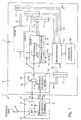
- the GPS type receiver with the correlation and demodulation circuit is Diagrammatically shown in Figure 1. It consists of an antenna 2 for receive GPS radio signals from multiple satellites, means for receiving and shaping the radio frequency signals 3 provided by the antenna 2, and a correlation and demodulation circuit 6 receiving signals intermediates IF in complex form at a frequency of the order of 400 kHz receiving means 3.
- a first electronic circuit 4 In the reception means 3, a first electronic circuit 4 'converts first of all the radio frequency signals of frequency 1,57542 GHz in one frequency for example 179 MHz.
- a second IF electronic circuit 4 "proceeds to a double conversion to bring the GPS signals first to a frequency of 4.76 MHz then finally at a frequency of 400 kHz sampling at 4.36 MHz.
- Intermediate IF complex signals sampled and quantized at a frequency of The order of 400 kHz is thus provided to the correlation and demodulation circuit.
- the complex IF intermediate signals are therefore composed of a signal in phase I and a quadrature signal Q shown in the figure by a line in bold cut a slash defining 2 bits. However, these IF intermediate signals could be set to 4 bits if a 2-bit conversion in a previous stage was operated, or 2n bits (n integer greater than 1).
- a signal generator clock 5 is part of the means for receiving and formatting the signals
- This generator is equipped, for example, with a non-crystal oscillator shown calibrated at a frequency of the order of 17.6 MHz.
- Two clock signals CLK and CLK16 are supplied to the correlation and demodulation circuit to clock all the operations of this circuit.
- the first clock frequency CLK can be worth 4.36 MHz, while the second clock rate can be fixed 16 times lower, ie 272.5 kHz used for a large part of the correlation in order to gain in energy consumption.
- the signals provided by the first circuit 4 give by example in half the cases of the signals of different parity (+1 and -1) with 2 bits output or (+3; +1; -1; -3) with 4 output bits. It must therefore be taken into account parity for the demodulation operations of the GPS signals in the receiver.
- Said correlation and demodulation circuit 6 comprises a stage of correlation 7 consisting of 12 channels 7 ', a data transfer bus 10 connecting each channel to a respective buffer register 11, and a data bus 13 connecting each buffer register to microprocessor means.
- memory 18 connected to the microprocessor are part of the microprocessor means 12 to store for example data relating to each satellite placed in orbit and carrier frequency parameter data and pseudo-random code of each satellite. All elements composing the correlation circuit and demodulation can be performed on a single semiconductor substrate, such as than a silicon substrate.
- test signal generation means 14 which comprise a test signal generator 15 and a multiplexer 16.
- the multiplexer 16 of the test signal generating means 14 receives at one input the intermediate signals IF supplied by the reception means 3 and at another input the intermediate IF test signals test .
- Said multiplexer 16 is controlled by a control signal Test supplied by control means integrated in the microprocessor means 12 through control buses 19 and a buffer register 11 '.
- the multiplexer 16 could also be integrated in the test signal generator 15 as needed.
- the IF intermediate signals representative of the radio frequency signals transmitted by several satellites are transmitted by the multiplexer 16 to the correlation stage 7 for all the channels 7 '.
- Some channels are configured differently in normal operation through the microprocessor 12 so that they each seek a visible satellite using IF intermediate signals to demodulate received GPS messages.
- the microprocessor 12 controls a test phase, it sends test control signals in particular to the means of generating test signals 14 via the control buses 19.
- the test signal generator 15 is therefore switched on, and the multiplexer 16 receiving the signal Test transmits only the IF test intermediate test signals produced by the generator 15 to the correlation stage 7. Said test signal generator will be explained in more detail for reference. in Figure 2.
- test signal generator 15 generates IF test intermediate test signals instead of traditional intermediate signals to perform a test representative of the closed loop correlation stage.
- These test IF test signals are modulated with a pseudo-random code of repetition length lower than the Gold code in order to perform a closed-loop test more quickly.
- the repetition length of the reduced pseudo-random code is 31 chips, that is to say 25 -1, whereas the Gold code is of a repetition length of 1023 chips, it is ie 2 10 -1.
- the repetition length of the second reduced pseudo-random code may be 2 (nm) -1, while the repetition length of the first pseudo code -random of the signals received is 2 n -1.
- the numbers n and m are integers with n greater than 3 and m taking a value between 1 and n-1.
- test selectors 17 each placed in a respective channel 7 '.
- Each channel 7 ' comprises a correlator 8 receiving the IF or IF test signals and preferably a controller 9 intended to activate by a dedicated equipment, in particular, a signal processing algorithm for acquiring the signal of a satellite and the tracking said satellite detected by the channel.
- the test selectors 17 each connected to a respective correlator 8 have the task of providing CS commands correlator correlator to configure including a pseudo-random code generator, which will be explained in more detail with reference to Figure 3b.
- the TMS control signals are in principle defined as a two-bit control word for normal operation or various test modes. If TMS is 00 in binary, then no test CS command is transmitted for normal operation. If TMS is 11 in binary, the closed-loop test mode is imposed to control the smooth operation of all the channels 7 'of the correlation stage 7 with the IF test intermediate test signals introduced at the input. If TMS is 01 in binary, a test of the correlator module 8 of each channel can be undertaken by means of a not shown test vector generator controlled by the microprocessor 12. If TMS is 10 in binary, a test of the controller module 9 of each channel can be undertaken through the test vector generator. In the present invention, the TMS signals preferably take the values 00 or 11.
- all the selectors 17 could be part of the microprocessor means 12.
- the commands CS for each correlator 8 could pass through buses 10 and 13.
- the microprocessor 12 transmits via the buses 13 and 10 parameters relating to the pseudo-random code to be searched, and to the carrier frequency of the intermediate test signals. These parameters are transmitted to configure all the channels 7 'in test phase as is also done in normal operation, but individually for each channel. However, during the test phase, the parameters are the same for all the channels so that the intermediate IF test signals with a single pseudo-random reduced code are processed in all the channels simultaneously and identically.
- the registers 11 of each channel are likely to receive data or parameters from configuration from microprocessor 12 and memory means 18 associated with it for each correlation channel 7 '.
- data concerning GPS messages, the status of the PRN code, the increment of frequency relative to the Doppler effect, pseudo-distances and other data can transmitted to the microprocessor 12 after the correlation and the lock on a specific satellite ..
- said registers 11 receive the results of the loop test closed, as well as the messages to be processed by the microprocessor.
- the microprocessor can therefore control following the test if all the correlation channels are working properly independent of the outside before putting the circuit back correlation and demodulation in normal operation.
- registers 11 can accumulate data during the correlation phase that will be used during the proceedings acquisition and tracking of satellites without necessarily being transferred automatically to the microprocessor 12.
- a single block of registers 11 can be considered for all the channels 7 'of the correlation stage, since some data placed in the block of registers are common to each channel.
- the microprocessor 12 may be reduced size.
- This microprocessor 12 may be for example a microprocessor 8-bit CooIRISC-816 from EM Microelectronic-Marin SA in Switzerland.
- a microprocessor of larger size for example a 32-bit microprocessor, could be used to avoid placing a controller 9 in each channel.
- This larger microprocessor should in this case take care of all tasks of satellite acquisition and tracking procedures in operation normal and in test phase according to the invention.
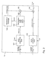
- FIG. 2 schematically shows the different blocks constituting the test signal generator 15.
- This test signal generator is triggered on the control of the microprocessor as explained above. As soon as it is switched on, it produces IF test intermediate test signals intended to be introduced into the correlation stage to be tested in a closed loop.
- the IF test noiseless test intermediate signals shall be designed equivalent to the intermediate signals derived from the radio frequency signals formed in the receiver.
- the intermediate test signals or substitution signals must be modulated with a pseudo-random code of length less than the Gold code in order to reduce the test time of the correlation stage.
- the test signal generator 15 comprises a numerically controlled 8-bit oscillator (NCO) 151 for the code clocked by the clock signals CLK, a small PRN code generator 152, a message generator 154, an oscillator 8- digitally controlled bit (NCO) 153 for the carrier clocked by the clock signals CLK and two signal mixers 155 and 156.
- the two 8-bit oscillators 151 and 153 have a frequency resolution of the order of 17 kHz which is defined by the CLK clock frequency of 4.36 MHz divided by 2 8 .
- the two 8-bit oscillators with numerical control 151 and Each receive an 8-bit binary word of the microprocessor.
- the first oscillator 151 receives a code increment to produce a clock signal PRN-CLKs to clock the small code generator PRN 152 that follows.
- the second oscillator 153 receives a carrier frequency increment to produce signals carrier, one signal is in phase and another signal is in quadrature.
- the value of the carrier frequency does not matter much for the loop test closed the correlation stage. As a result, this carrier frequency can take a value of 400 kHz as the traditional intermediate signals, or a value lower.
- the small PRN code generator 152 receives the PRN-CLKs clock signal from the oscillator 151 to produce a pseudo-random code of reduced repetition length.
- the repeat length of this code is preferably 31, that is to say May 2 -1 as explained above.
- the frequency of the PRN-CLKs clock signal is a function of the increment of code entered at the input of the digitally controlled oscillator 151. If the increment of code is set to a value of 24, which gives 11000 in binary, the frequency clock PRN-CLKs is 24 times 17 kHz, that is to say 408 kHz.
- the code increment could obviously be set higher so as to approach the frequency of 1.023 MHz for a correlation stage code generator in operation normal. However, the 408 kHz value of the PRN-CLKs frequency was chosen in order to get closer in the test phase of the actual treatment of said floor of correlation in normal operation.
- the output signals of the correlation stage must be equivalent whether intermediate signals traditional, which include a noise about 16 dB higher than the useful signals, or noise-free intermediate test signals supplied to the input of the stage of correlation.
- the purpose is to take into account the noise inherent in radio frequency signals to do a quick test close to the reality of the correlation stage with the signals test without noise.
- a message generator 154 is clocked by a period signal (1 ms) to give a message at 50 Hz (modulo 20-epoch).
- the message generator message 154 and the reduced PRN code of the small PRN generator 152 are mixed in the mixer 155.
- the output of this mixer 155 is also mixed or modulated on the loop carrier in the mixer 156 to produce the intermediate signals of the mixer. IF test .
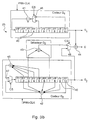
- Figure 3a shows in more detail the small pseudo-random code generator 152, the structure of which is well known to those skilled in the art. Since it must produce a code length of 31, it comprises in a G 1S encoder and in a G 2S encoder a series of five flip-flops defined by the symbol FF and the number of each flip-flop. A transfer of the state of each flip-flop 30 is generated from flip-flop FF1 to flip-flop FF5 at each clock stroke PRN-CLKs.
- the flip-flops FF3 and FF5 each have an output added in the adder 34 of the EX-OR type.
- the output of the adder 34 is introduced into the flip-flop FF1 in order to produce a first coded signal G 1S at the output of the last flip-flop FF5 at each clock pulse PRN-CLKs.
- the flip-flops FF2 to FF5 each have an output added in the adder 32 of the EX-OR type.
- the output of the adder 32 is introduced into the flip-flop FF1 in order to produce a second coded signal G 2S at the output of the last flip-flop FF5 at each clock pulse PRN-CLKs.
- the first and second coded signals G 1S and G 2S are also added in an adder 33 of the EX-OR type in order to produce the coded signal Gs which corresponds to the output signal of the small code generator PRN 152.
- Figure 3b shows a traditional pseudo-random code generator used in each correlator of the correlation stage.
- the structure of this generator is well known to those skilled in this technical field for the purpose of producing a replica of the Gold code in normal operation.
- this code generator 25 additionally comprises multiplexers 46 to 48 in order to be able to configure said generator also in test phase. In the testing phase, the code generator 25 must be configured to produce a pseudo-random code replica generated in the test signal generator, that is to say a run length code equal to 31 (2 5 - 1).
- the pseudo-random code generator 25 comprises a first encoder G 1 in which ten flip-flops 40, defined by the symbol FF and the number of each flip-flop, are placed in series, a second encoder G 2 in which also ten latches are placed in series, and a selector G 2 with time shift to define the specific code of a satellite.
- the flip-flops FF3 and FF10 of the encoder G 1 each have an output added to the adder 41 of the EX-OR type.
- the output signal of the flip-flop FF10 passes freely (shown in dotted lines in the figure) by the multiplexer 46 if no command CS is imposed on said multiplexer 46.
- the output of the adder 41 is introduced at the input of the flip-flop 40 FF1 to produce a first coded signal G 1 at the output of the last flip-flop FF10 at each clock stroke PRN-CLK.
- This PRN-CLK clock signal is worth about 1.023 MHz in normal operation, while in test phase it should be about 408 kHz depending on the intermediate test signals.
- a command CS is imposed on the multiplexer 46 so that only the outputs of the flip-flops 40 FF3 and FF5 are added in the adder 41.
- This configuration corresponds to the encoder G 1S , explained with reference to FIG. 3a, for produce a G 1S output signal.
- the flip-flops FF2, FF3, FF6, FF8, FF9 and FF10 each have an output added in the adder 42 of the EX-OR type.
- the output of the adder 42 is introduced at the input of the first flip-flop 40 FF1 through the multiplexer 47.
- the output of the adder 42 passes freely (shown in dashed lines in the figure) through the multiplexer 47 if no CS command is imposed on said multiplexer 47.
- a second coded signal G 2 is thus produced at the output of the last flip-flop 40 FF10 of the second coder G 2 at each clock stroke PRN-CLK.
- the outputs of the flip-flops FF2 to FF5 of the coder G 2 are introduced into the adder 45 of the EX-OR type, the output of which is placed at the input of the multiplexer 47.
- a command CS is imposed on the multiplexer 47 in order to that the output of the adder 45 is introduced at the input of the first flip-flop FF1 in place of the output of the adder 42.
- This configuration corresponds to the coder G 2S , explained with reference to FIG. 3a, to produce a G 2S output signal.
- the selector G 2 comprises in particular an adder 43 of the EX-OR type which adds the output signals of two flip-flops chosen from the ten flip-flops 40, for example flip-flops 40 FF3 and FF7 of the second coder G 2 , for the production of the specific code. of a specific satellite.
- the addition by the adder 43 of the selector G 2 also generates a delay which is well known to those skilled in this technical field.
- the output of this adder 43 passes freely (shown in dashed lines in the figure) through a multiplexer 48 if no command CS is imposed on said multiplexer 48.
- the output of the selector G 2 can be added together with the output G 1 in an adder 44 of the EX-OR type to give the output signal G.
- the output G defines the generation of a replica of the specific gold code for a given satellite.
- a command CS is imposed on the multiplexer 48 so that only the outputs G 1 and G 2 are added in the adder 44 to produce a signal that corresponds to the signal G S explained with reference to Figure 3a.
- Figure 4 shows the different electronic elements of a correlator of the correlation stage which is well known to a person skilled in this field technical.
- the reader will refer to the teaching from the book “Understanding GPS Principles and Applications "in Chapter 5 by Phillip Ward and Editor Elliott D. Kaplan (Artech House Publishers, USA 1996) at ISBN 0-89006-793-7, and especially in Figures 5.8 and 5.13 which broadly represent all elements of Figure 4.
- the lines represented in bold with a slash define a number of bits in parallel.
- the correlator comprises a carrier mixer 20, a code mixer 21, counter integrators 22, code 23 and carrier 26 discriminators, digitally controlled oscillators of the code 24 and the carrier 27, a pseudo-random code generator 25, and a sin / cos table 28 of the carrier.
- the carrier mixer 20 receives at the input either the intermediate IF signals in normal operation, shown by a dashed line, or the IF test intermediate test signals in the test phase.
- These intermediate signals are complex signals, that is to say that they are composed of a signal in phase I and a quadrature signal Q according to the formula (I + iQ).
- the choice of the signals arriving at the mixer 20 is imposed by the microprocessor control means as explained above.
- These intermediate signals are processed in a servo loop of the PRN code and in a servo control loop of the carrier.
- the intermediate IF test signals are multiplied firstly by the cosine minus one sine of the replica of the carrier generated internally in order to draw the intermediate signal complex phase I signal, and other on the other hand by the least Sinus minus i times the cosine of the internally generated replica of the carrier in order to derive complex intermediate signals from the Q quadrature signal.
- the I and Q signals are input to a code mixer 21 to find the equivalence of the PRN code with the internally generated one.
- the signals in phase I and in quadrature Q are each multiplied, on the one hand, by an early replica E (of the English term "early") of the PRN code and, on the other hand, by a late replica L (of the English term "late” ) Of the PRN code to give four output signals I E , I L , Q E and Q L.
- E of the English term "early”
- a late replica L of the English term "late”
- the four correlated signals I E , I L , Q E and Q L are input into counter integrators 22 which are pre-detection elements.
- the four I ES , I LS , Q ES and Q LS output values of the counter integrators 22 are represented by 10 bits, which corresponds to a complete cycle of the Gold code. However, only 8 most significant bits of each output value are used in the code and carrier loop loops.
- the counter integrators 22 start the count following the beginning or the end of each code sequence.
- the time gain to obtain the values of output which corresponds to the ratio of integration times, ie (1 ms / 76 ⁇ s), multiplied by the repetition length ratio of the code, i.e. 1023/31.
- the time saving of the closed-loop test of the correlation and demodulation circuit is about 435 times less than the test time achieved if the pseudo-random code is of 1023 of repetition length. This gain could even be over 1000 times lower if the clock frequency of the code in the test phase was set to 1.023 MHz, because the integration time would go from 76 ⁇ s to about 31 ⁇ s.
- Two other output values I PS and Q PS corresponding to the pseudo-point values are obtained by adding the two output signals I ES and I LS for the value I PS , and the two signals Q ES and Q LS for the value Q PS .
- the four output signals I ES , I LS , Q ES and Q LS are introduced into a code discriminator 23 which performs the operations of calculating the energy of said output signals.
- NCO digitally controlled oscillator
- This phase loop increment adjusts the phase for generating the code replica.
- This oscillator 24 thus receives a binary word for example of 28 bits filtered from the discriminator 23.
- a phase increment of the code INCR-C is provided through the microprocessor and input registers and parameter output to set the starting value of the clock frequency of the code that must provide the oscillator 24.
- the value of this increment INCR-C is different if the circuit is in normal operating mode or test phase.
- the PRN-CLK clock frequency signal is supplied to the code generator PRN 25 to clock the generation of replicas early and late code pseudorandom. If a CS command is imposed on the code generator 25, this means that the generator is configured in test phase to generate a replica of the repetition length code equal to 31. Similarly in the test phase, the increment INCR-C supplied to the digitally controlled oscillator 24 is such that the frequency PRN-CLK clock output of the oscillator is preferably 408 kHz.
- the pseudo-point output signals I PS and Q PS are introduced into the carrier discriminator 26.
- NCO carrier digital control
- This carrier loop increment allows to adjust the frequency for the generation of the replica of the carrier.
- This oscillator 27 thus receives a binary word for example 24-bit filtered from the discriminator 26.
- a INCR-P frequency increment is introduced via in particular the microprocessor.
- the INCR-P frequency increment allows you to set initially the carrier frequency generated by the oscillator 27 to a value comparable to the carrier frequency of the intermediate signals.
- the value of this increment INCR-P is different if the circuit is in normal operation or in test phase.
- the output signals of the digitally controlled oscillator 27 are provided at a sin / cos table 28 so that the latter give two complex signals to the mixer 20.
- Complex signals (Cosx-iSinx) and (-Sinx-iCosx) are multiplied in the mixer 20 to complex intermediate signals to provide a signal in phase I and a Q quadrature signal.
- choosing a repetition length at 31 chips for the modulated pseudo-random code on the intermediate test signals allows, in the circuit test phase, to take into account a noise inherent in the signals radio frequencies with repetition length code of 1023 chips.
- the intermediate test signals therefore produce output signals from the counter integrators with output power comparable to the output power of the actual radio frequency signals which include noise. This therefore makes it possible to perform a closed-loop functional test close to the reality of the correlation stage with noise-free test signals with pseudo-random code reduced to 31.
- the message of the intermediate signals are demodulated in each output channel of the meter integrators 22 to provide the data to the microprocessor.
- the microprocessor can control the good functionality of each channel of the correlation stage. Thanks to the reduction of the repetition length of the code pseudo-random, the test time is greatly reduced while guaranteeing a test in closed loop comparable to a real functionality test. More than 90% of the elements can be tested in this closed-loop test mode.
- This closed-loop test operation may be repeated for periods of determined time, as explained above, according to a programming of microprocessor means.
- this programming is useful when the receiver with the correlation and demodulation circuit, which includes the test signal generator, is mounted in a portable object powered by a battery or accumulator.
- This portable object can of course to be a watch or a mobile phone for example in which it is necessary to save energy consumption even during the test phase.
- the circuit configurable in normal operation mode and in test mode can be used in any signal receiver modulated by a repetition length code determined.
- Intermediate test signals can be provided by a generator of test signals that are for example on the test bench rather than this generator is integrated in the circuit.
- the signal generator of test includes only about forty logical gates or flip-flop, while the circuit has nearly 2 million transistors, this represents only a tiny additional place on the circuit.
Landscapes
- Engineering & Computer Science (AREA)
- Remote Sensing (AREA)
- Computer Networks & Wireless Communication (AREA)
- Radar, Positioning & Navigation (AREA)
- Physics & Mathematics (AREA)
- Electromagnetism (AREA)
- Signal Processing (AREA)
- General Physics & Mathematics (AREA)
- Position Fixing By Use Of Radio Waves (AREA)
- Radar Systems Or Details Thereof (AREA)
- Circuits Of Receivers In General (AREA)
- Radio Relay Systems (AREA)
- Monitoring And Testing Of Transmission In General (AREA)
Description
- la figure 1 représente schématiquement un récepteur de signaux radiofréquences avec un circuit de corrélation et de démodulation selon l'invention,
- la figure 2 représente schématiquement les éléments électroniques du générateur de signaux de test du circuit selon l'invention,
- la figure 3a représente un générateur de code PRN réduit des moyens de génération des signaux de tests du circuit selon l'invention,
- la figure 3b représente un générateur de code PRN configurable en mode de fonctionnement normal et en mode de test de chaque canal de l'étage de corrélation du circuit selon l'invention, et
- la figure 4 représente schématiquement les éléments d'un corrélateur de l'étage de corrélation du circuit selon l'invention.
Claims (13)
- Circuit de corrélation et de démodulation (6) d'un récepteur (1) de signaux modulés par un premier code d'une longueur de répétition déterminée, ledit premier code définissant une source émettrice desdits signaux, ledit circuit comprenant un étage de corrélation (7) relié à des moyens de commande (12) notamment pour configurer ledit étage de corrélation en mode de fonctionnement normal ou en mode de test, en fonctionnement normal ledit étage étant destiné à recevoir des signaux intermédiaires (IF) correspondant aux signaux modulés mis en forme dans des moyens de réception (3) des signaux modulés du récepteur, lesdits signaux intermédiaires étant corrélés dans une boucle d'asservissement d'un corrélateur (8) dudit étage de corrélation (7) avec une réplique du premier code fournie par un générateur de code (25), caractérisé en ce qu'en phase de test, ledit générateur de code (25) est adapté par l'intermédiaire des moyens de commande (12) pour générer une réplique d'un second code de longueur de répétition inférieure au premier code pour des opérations de corrélation avec des signaux intermédiaires de test (IFtest) modulés par le second code de longueur de répétition inférieure au premier code et fournis à l'étage de corrélation (7) de manière à opérer un test représentatif de fonctionnement en boucle fermée de l'étage de corrélation plus rapidement qu'avec des signaux modulés par le premier code.
- Circuit de corrélation et de démodulation (6) selon la revendication 1, caractérisé en ce qu'il comprend un générateur de signaux de test (15) susceptible de fournir en phase de test les signaux intermédiaires de test (IFtest) à l'étage de corrélation en lieu et place de signaux intermédiaires (IF) du récepteur, lesdits signaux de test étant modulés par le second code de longueur de répétition inférieure au premier code de manière à opérer un test représentatif de fonctionnement en boucle fermée de l'étage de corrélation (7).
- Circuit de corrélation et de démodulation (6) selon la revendication 2 pour un récepteur (1) de signaux radiofréquences, le premier code étant un premier code pseudo-aléatoire différent pour chaque satellite émetteur, caractérisé en ce que le générateur de signaux de test (15) fournit en phase de test des signaux de test (IFtest) modulés par un second code pseudo-aléatoire de longueur de répétition inférieure au premier code pseudo-aléatoire, et en ce que le générateur de code (25) est adapté par l'intermédiaire des moyens de commande (12) pour produire une réplique du second code pseudo-aléatoire pour les opérations de corrélation en phase de test avec les signaux de test.
- Circuit de corrélation et de démodulation (6) selon la revendication 3 pour un récepteur (1) de type GPS, caractérisé en ce que les moyens de commande font partie de moyens à microprocesseur (12, 18) susceptible de calculer des données de position, de vitesse et temporelles, d'adapter des paramètres de boucle d'asservissement au début des opérations de corrélation et de contrôler le bon fonctionnement de l'étage de corrélation en phase de test.
- Circuit de corrélation et de démodulation (6) selon l'une des revendications 3 et 4, caractérisé en ce que l'étage de corrélation (7) comprend plusieurs canaux (7') dont chacun est muni d'un corrélateur (8) pour permettre d'acquérir et de poursuivre plusieurs satellites visibles simultanément en fonctionnement normal, alors qu'en phase de test tous les canaux de l'étage de corrélation, dans lesquels chaque générateur de code (25) est adapté pour générer une même réplique du second code, reçoivent uniquement les signaux de test (IFtest) du générateur de signaux de test (15) afin de contrôler simultanément le bon fonctionnement des opérations de corrélation de tous les canaux de l'étage de corrélation.
- Circuit de corrélation et de démodulation (6) selon la revendication 4, caractérisé en ce que le microprocesseur (12) est programmé de telle manière à commander la phase de test de l'étage de corrélation (7) par périodes de temps prédéterminées.
- Circuit de corrélation et de démodulation (6) selon l'une des revendications 3 à 6, caractérisé en ce que le générateur de signaux de test (15) produit, en phase de test, des signaux de test à fréquence porteuse modulés par le second code pseudo-aléatoire dont la longueur de répétition est déterminée de telle manière à tenir compte, dans des boucles d'asservissement relatives à la fréquence porteuse et au code pseudo-aléatoire de l'étage de corrélation, d'un bruit inhérent des signaux radiofréquences modulés par le premier code pseudo-aléatoire, afin d'avoir une puissance comparable sur des signaux de sortie d'éléments de pré-détection, tels que des intégrateurs compteurs (22).
- Circuit de corrélation et de démodulation (6) selon la revendication 7, caractérisé en ce que les moyens à microprocesseur (12) définissent en collaboration avec le générateur de code (25) de chaque canal de l'étage de corrélation la durée d'intégration des éléments de pré-détection en fonction de la longueur de répétition du premier ou du second code pseudo-aléatoire.
- Circuit de corrélation et de démodulation (6) selon l'une des revendications 3 et 7, caractérisé en ce que le générateur de signaux de test (15) comprend un générateur de second code pseudo-aléatoire, un premier oscillateur à commande numérique (151), tel qu'un oscillateur 8-bit, pour fournir des signaux d'horloge (PRN-CLKs) au générateur du second code pseudo-aléatoire (152) sur la base d'un premier mot binaire fourni par les moyens à microprocesseur, un second oscillateur à commande numérique (153), tel qu'un oscillateur 8-bit, pour générer des signaux à fréquence porteuse sur la base d'un second mot binaire fourni par les moyens à microprocesseur, le second code pseudo-aléatoire étant modulé sur lesdits signaux à fréquence porteuse, et un générateur de message (154) dont les signaux de message sont également modulés sur les signaux à fréquence porteuse, l'étage de corrélation (7) étant destiné à fournir les données de message de test aux moyens à microprocesseur pour le contrôle en phase de test du fonctionnement en boucle fermée de l'étage de corrélation.
- Circuit de corrélation et de démodulation (6) selon l'une des revendications 7 et 9, caractérisé en ce que le second code pseudo-aléatoire réduit est de longueur de répétition égale à 31, alors que le premier code pseudo-aléatoire des signaux radiofréquences est de longueur de répétition égale à 1023 permettant de fournir en sortie des éléments de pré-détection (22) de l'étage de corrélation des signaux (IES, ILS, QES, QLS) comparables en tenant compte d'un bruit inhérent aux signaux radiofréquences.
- Circuit de corrélation et de démodulation (6) selon l'une des revendications 3 à 5, caractérisé en ce que l'étage de corrélation (7) comprend, pour chaque canal (7'), un contrôleur (9) relié au corrélateur (8) pour mettre en oeuvre un algorithme de traitement des signaux numériques dans toutes les tâches de synchronisation afin d'ajuster notamment des paramètres de phase et/ou de fréquence pour le générateur de code (25) dans un mode de fonctionnement normal ou dans un mode de test.
- Circuit de corrélation et de démodulation (6) selon la revendication 5, caractérisé en ce que le corrélateur (8) de chaque canal de l'étage de corrélation (7) comprend des moyens de génération (27, 28) d'une réplique de signaux à fréquence porteuse pouvant être adapté par les moyens à microprocesseur (12) dans un mode de fonctionnement normal ou un mode de test, en fonction de la fréquence porteuse des signaux intermédiaires fournis au corrélateur.
- Circuit de corrélation et de démodulation (6) selon l'une des revendications précédentes, caractérisé en ce que tous les éléments dudit circuit sont réalisés sur un unique substrat semi-conducteur, tel qu'un substrat en silicium.
Priority Applications (3)
| Application Number | Priority Date | Filing Date | Title |
|---|---|---|---|
| AT00204605T ATE314662T1 (de) | 2000-12-18 | 2000-12-18 | Schaltung zur korrelation und demodulation eines empfängers von signalen moduliert mit einem spezifischen kode |
| EP00204605A EP1215505B1 (fr) | 2000-12-18 | 2000-12-18 | Circuit de corrélation et de démodulation d'un récepteur de signaux modulés par un code spécifique |
| DE60025232T DE60025232T2 (de) | 2000-12-18 | 2000-12-18 | Schaltung zur Korrelation und Demodulation eines Empfängers von Signalen, modulert mit einem spezifischen Kode |
Applications Claiming Priority (1)
| Application Number | Priority Date | Filing Date | Title |
|---|---|---|---|
| EP00204605A EP1215505B1 (fr) | 2000-12-18 | 2000-12-18 | Circuit de corrélation et de démodulation d'un récepteur de signaux modulés par un code spécifique |
Publications (2)
| Publication Number | Publication Date |
|---|---|
| EP1215505A1 EP1215505A1 (fr) | 2002-06-19 |
| EP1215505B1 true EP1215505B1 (fr) | 2005-12-28 |
Family
ID=8172453
Family Applications (1)
| Application Number | Title | Priority Date | Filing Date |
|---|---|---|---|
| EP00204605A Expired - Lifetime EP1215505B1 (fr) | 2000-12-18 | 2000-12-18 | Circuit de corrélation et de démodulation d'un récepteur de signaux modulés par un code spécifique |
Country Status (3)
| Country | Link |
|---|---|
| EP (1) | EP1215505B1 (fr) |
| AT (1) | ATE314662T1 (fr) |
| DE (1) | DE60025232T2 (fr) |
Family Cites Families (2)
| Publication number | Priority date | Publication date | Assignee | Title |
|---|---|---|---|---|
| US4100531A (en) * | 1977-02-03 | 1978-07-11 | Nasa | Bit error rate measurement above and below bit rate tracking threshold |
| US5093800A (en) * | 1989-09-14 | 1992-03-03 | Saburo Ifune | Global positioning system satellite signal simulator |
-
2000
- 2000-12-18 DE DE60025232T patent/DE60025232T2/de not_active Expired - Lifetime
- 2000-12-18 EP EP00204605A patent/EP1215505B1/fr not_active Expired - Lifetime
- 2000-12-18 AT AT00204605T patent/ATE314662T1/de not_active IP Right Cessation
Also Published As
| Publication number | Publication date |
|---|---|
| DE60025232D1 (de) | 2006-02-02 |
| ATE314662T1 (de) | 2006-01-15 |
| EP1215505A1 (fr) | 2002-06-19 |
| DE60025232T2 (de) | 2006-10-19 |
Similar Documents
| Publication | Publication Date | Title |
|---|---|---|
| CA2645542C (fr) | Generateur de code adaptatif pour des recepteurs de navigation par satellite | |
| EP0856162B1 (fr) | Recepteur de determination d'une position a partir de reseaux de satellites | |
| EP0806679B1 (fr) | Dispositif de réception pour système de navigation notamment par satellite | |
| CN101356449B (zh) | 为接收自多种卫星系统的卫星信号执行信号相关的方法和装置 | |
| JP4047582B2 (ja) | 特有のコードで変調された信号用受信器の相関および復調回路 | |
| EP2323271B1 (fr) | Procédé d'acquisition de signaux de radionavigation à code d'étalement à période quasi-infinie | |
| CA2674544C (fr) | Procede et dispositif de reception d'un signal de radionavigation a modulation boc | |
| FR2856143A1 (fr) | Procede et dispositif de demodulation de signaux de radionavigation par satellite | |
| FR2783929A1 (fr) | Procede et dispositif de traitement en reception d'un signal l2 de satellite gps | |
| EP1628139B1 (fr) | Procédé de détermination de position d'un récepteur de signaux radiofréquences sans connaissance de la position initiale, et récepteur pour sa mise en oeuvre | |
| EP1170597B1 (fr) | Récepteur GPS basse puissance avec redistribution de tâches de synchronisation | |
| EP1215505A1 (fr) | Circuit de corrélation et de démodulation d'un récepteur de signaux modulés par un code spécifique | |
| EP1265371B1 (fr) | Récepteur et procédé de reception de signaux radiofréquences avec des moyens de correction des effets des signaux à trajets multiplex | |
| EP2068168A1 (fr) | Procédé de détermination d'une position d'un récepteur de signaux radiofréquences basse puissance | |
| EP0921409B1 (fr) | Récepteur GPS bi-fréquence, opératoire sur toutes les mesures en présence d'encryptage | |
| JP2003087222A (ja) | スペクトラム拡散信号復調方法および装置 | |
| RU227214U1 (ru) | Микросхема навигационного процессора | |
| EP1215557B1 (fr) | Oscillateur à commande numérique notamment pour un récepteur de signaux radiofréquences | |
| EP1255123B1 (fr) | Récepteur de signaux radiofréquences ayant des moyens pour améliorer la dynamique de réception desdits signaux | |
| EP1400028B1 (fr) | Module discriminateur de trajets multiples pour un systeme de navigation. |
Legal Events
| Date | Code | Title | Description |
|---|---|---|---|
| PUAI | Public reference made under article 153(3) epc to a published international application that has entered the european phase |
Free format text: ORIGINAL CODE: 0009012 |
|
| AK | Designated contracting states |
Kind code of ref document: A1 Designated state(s): AT BE CH CY DE DK ES FI FR GB GR IE IT LI LU MC NL PT SE TR |
|
| AX | Request for extension of the european patent |
Free format text: AL;LT;LV;MK;RO;SI |
|
| 17P | Request for examination filed |
Effective date: 20021219 |
|
| AKX | Designation fees paid |
Designated state(s): AT BE CH CY DE DK ES FI FR GB GR IE IT LI LU MC NL PT SE TR |
|
| GRAP | Despatch of communication of intention to grant a patent |
Free format text: ORIGINAL CODE: EPIDOSNIGR1 |
|
| GRAS | Grant fee paid |
Free format text: ORIGINAL CODE: EPIDOSNIGR3 |
|
| GRAA | (expected) grant |
Free format text: ORIGINAL CODE: 0009210 |
|
| AK | Designated contracting states |
Kind code of ref document: B1 Designated state(s): AT BE CH CY DE DK ES FI FR GB GR IE IT LI LU MC NL PT SE TR |
|
| PG25 | Lapsed in a contracting state [announced via postgrant information from national office to epo] |
Ref country code: IE Free format text: LAPSE BECAUSE OF FAILURE TO SUBMIT A TRANSLATION OF THE DESCRIPTION OR TO PAY THE FEE WITHIN THE PRESCRIBED TIME-LIMIT Effective date: 20051228 Ref country code: AT Free format text: LAPSE BECAUSE OF FAILURE TO SUBMIT A TRANSLATION OF THE DESCRIPTION OR TO PAY THE FEE WITHIN THE PRESCRIBED TIME-LIMIT Effective date: 20051228 Ref country code: IT Free format text: LAPSE BECAUSE OF FAILURE TO SUBMIT A TRANSLATION OF THE DESCRIPTION OR TO PAY THE FEE WITHIN THE PRE;WARNING: LAPSES OF ITALIAN PATENTS WITH EFFECTIVE DATE BEFORE 2007 MAY HAVE OCCURRED AT ANY TIME BEFORE 2007. THE CORRECT EFFECTIVE DATE MAY BE DIFFERENT FROM THE ONE RECORDED.SCRIBED TIME-LIMIT Effective date: 20051228 |
|
| REG | Reference to a national code |
Ref country code: GB Ref legal event code: FG4D Free format text: NOT ENGLISH |
|
| REG | Reference to a national code |
Ref country code: CH Ref legal event code: EP |
|
| REG | Reference to a national code |
Ref country code: IE Ref legal event code: FG4D Free format text: LANGUAGE OF EP DOCUMENT: FRENCH |
|
| REF | Corresponds to: |
Ref document number: 60025232 Country of ref document: DE Date of ref document: 20060202 Kind code of ref document: P |
|
| PG25 | Lapsed in a contracting state [announced via postgrant information from national office to epo] |
Ref country code: SE Free format text: LAPSE BECAUSE OF FAILURE TO SUBMIT A TRANSLATION OF THE DESCRIPTION OR TO PAY THE FEE WITHIN THE PRESCRIBED TIME-LIMIT Effective date: 20060328 Ref country code: GR Free format text: LAPSE BECAUSE OF FAILURE TO SUBMIT A TRANSLATION OF THE DESCRIPTION OR TO PAY THE FEE WITHIN THE PRESCRIBED TIME-LIMIT Effective date: 20060328 Ref country code: DK Free format text: LAPSE BECAUSE OF FAILURE TO SUBMIT A TRANSLATION OF THE DESCRIPTION OR TO PAY THE FEE WITHIN THE PRESCRIBED TIME-LIMIT Effective date: 20060328 |
|
| PG25 | Lapsed in a contracting state [announced via postgrant information from national office to epo] |
Ref country code: ES Free format text: LAPSE BECAUSE OF FAILURE TO SUBMIT A TRANSLATION OF THE DESCRIPTION OR TO PAY THE FEE WITHIN THE PRESCRIBED TIME-LIMIT Effective date: 20060408 |
|
| REG | Reference to a national code |
Ref country code: CH Ref legal event code: NV Representative=s name: ICB INGENIEURS CONSEILS EN BREVETS SA |
|
| GBT | Gb: translation of ep patent filed (gb section 77(6)(a)/1977) |
Effective date: 20060327 |
|
| PG25 | Lapsed in a contracting state [announced via postgrant information from national office to epo] |
Ref country code: PT Free format text: LAPSE BECAUSE OF FAILURE TO SUBMIT A TRANSLATION OF THE DESCRIPTION OR TO PAY THE FEE WITHIN THE PRESCRIBED TIME-LIMIT Effective date: 20060529 |
|
| REG | Reference to a national code |
Ref country code: IE Ref legal event code: FD4D |
|
| PLBE | No opposition filed within time limit |
Free format text: ORIGINAL CODE: 0009261 |
|
| STAA | Information on the status of an ep patent application or granted ep patent |
Free format text: STATUS: NO OPPOSITION FILED WITHIN TIME LIMIT |
|
| 26N | No opposition filed |
Effective date: 20060929 |
|
| PG25 | Lapsed in a contracting state [announced via postgrant information from national office to epo] |
Ref country code: BE Free format text: LAPSE BECAUSE OF NON-PAYMENT OF DUE FEES Effective date: 20061231 Ref country code: MC Free format text: LAPSE BECAUSE OF NON-PAYMENT OF DUE FEES Effective date: 20061231 |
|
| BERE | Be: lapsed |
Owner name: ASULAB S.A. Effective date: 20061231 |
|
| PG25 | Lapsed in a contracting state [announced via postgrant information from national office to epo] |
Ref country code: LU Free format text: LAPSE BECAUSE OF NON-PAYMENT OF DUE FEES Effective date: 20061218 Ref country code: TR Free format text: LAPSE BECAUSE OF FAILURE TO SUBMIT A TRANSLATION OF THE DESCRIPTION OR TO PAY THE FEE WITHIN THE PRESCRIBED TIME-LIMIT Effective date: 20051228 |
|
| PG25 | Lapsed in a contracting state [announced via postgrant information from national office to epo] |
Ref country code: CY Free format text: LAPSE BECAUSE OF FAILURE TO SUBMIT A TRANSLATION OF THE DESCRIPTION OR TO PAY THE FEE WITHIN THE PRESCRIBED TIME-LIMIT Effective date: 20051228 |
|
| PGFP | Annual fee paid to national office [announced via postgrant information from national office to epo] |
Ref country code: NL Payment date: 20081125 Year of fee payment: 9 |
|
| PGFP | Annual fee paid to national office [announced via postgrant information from national office to epo] |
Ref country code: GB Payment date: 20081125 Year of fee payment: 9 |
|
| PGFP | Annual fee paid to national office [announced via postgrant information from national office to epo] |
Ref country code: FI Payment date: 20091126 Year of fee payment: 10 Ref country code: CH Payment date: 20091125 Year of fee payment: 10 |
|
| PGFP | Annual fee paid to national office [announced via postgrant information from national office to epo] |
Ref country code: IT Payment date: 20081218 Year of fee payment: 9 |
|
| PGRI | Patent reinstated in contracting state [announced from national office to epo] |
Ref country code: IT Effective date: 20091201 |
|
| PGFP | Annual fee paid to national office [announced via postgrant information from national office to epo] |
Ref country code: FR Payment date: 20100115 Year of fee payment: 10 |
|
| PGFP | Annual fee paid to national office [announced via postgrant information from national office to epo] |
Ref country code: DE Payment date: 20091204 Year of fee payment: 10 |
|
| REG | Reference to a national code |
Ref country code: NL Ref legal event code: V1 Effective date: 20100701 |
|
| GBPC | Gb: european patent ceased through non-payment of renewal fee |
Effective date: 20091218 |
|
| PG25 | Lapsed in a contracting state [announced via postgrant information from national office to epo] |
Ref country code: NL Free format text: LAPSE BECAUSE OF NON-PAYMENT OF DUE FEES Effective date: 20100701 |
|
| PG25 | Lapsed in a contracting state [announced via postgrant information from national office to epo] |
Ref country code: GB Free format text: LAPSE BECAUSE OF NON-PAYMENT OF DUE FEES Effective date: 20091218 |
|
| PG25 | Lapsed in a contracting state [announced via postgrant information from national office to epo] |
Ref country code: IT Free format text: LAPSE BECAUSE OF NON-PAYMENT OF DUE FEES Effective date: 20091218 |
|
| REG | Reference to a national code |
Ref country code: CH Ref legal event code: PL |
|
| PG25 | Lapsed in a contracting state [announced via postgrant information from national office to epo] |
Ref country code: FI Free format text: LAPSE BECAUSE OF NON-PAYMENT OF DUE FEES Effective date: 20101218 |
|
| REG | Reference to a national code |
Ref country code: FR Ref legal event code: ST Effective date: 20110831 |
|
| PG25 | Lapsed in a contracting state [announced via postgrant information from national office to epo] |
Ref country code: CH Free format text: LAPSE BECAUSE OF NON-PAYMENT OF DUE FEES Effective date: 20101231 Ref country code: FR Free format text: LAPSE BECAUSE OF NON-PAYMENT OF DUE FEES Effective date: 20110103 Ref country code: LI Free format text: LAPSE BECAUSE OF NON-PAYMENT OF DUE FEES Effective date: 20101231 |
|
| REG | Reference to a national code |
Ref country code: DE Ref legal event code: R119 Ref document number: 60025232 Country of ref document: DE Effective date: 20110701 |
|
| PG25 | Lapsed in a contracting state [announced via postgrant information from national office to epo] |
Ref country code: DE Free format text: LAPSE BECAUSE OF NON-PAYMENT OF DUE FEES Effective date: 20110701 |