EP1213823A2 - DC-to-DC converter - Google Patents
DC-to-DC converter Download PDFInfo
- Publication number
- EP1213823A2 EP1213823A2 EP01128657A EP01128657A EP1213823A2 EP 1213823 A2 EP1213823 A2 EP 1213823A2 EP 01128657 A EP01128657 A EP 01128657A EP 01128657 A EP01128657 A EP 01128657A EP 1213823 A2 EP1213823 A2 EP 1213823A2
- Authority
- EP
- European Patent Office
- Prior art keywords
- circuit
- switch
- converter
- load magnitude
- reference period
- Prior art date
- Legal status (The legal status is an assumption and is not a legal conclusion. Google has not performed a legal analysis and makes no representation as to the accuracy of the status listed.)
- Granted
Links
- 238000009499 grossing Methods 0.000 claims abstract description 20
- 230000001960 triggered effect Effects 0.000 claims description 8
- 238000004804 winding Methods 0.000 abstract description 12
- 230000009467 reduction Effects 0.000 abstract description 5
- 238000010586 diagram Methods 0.000 description 20
- 238000010276 construction Methods 0.000 description 10
- 239000003990 capacitor Substances 0.000 description 6
- 230000008859 change Effects 0.000 description 6
- 230000004044 response Effects 0.000 description 6
- 230000004048 modification Effects 0.000 description 5
- 238000012986 modification Methods 0.000 description 5
- 238000004519 manufacturing process Methods 0.000 description 4
- 238000001514 detection method Methods 0.000 description 3
- 238000000034 method Methods 0.000 description 3
- 238000013461 design Methods 0.000 description 2
- 238000007689 inspection Methods 0.000 description 2
- 230000003287 optical effect Effects 0.000 description 2
- 238000006467 substitution reaction Methods 0.000 description 2
- 230000007704 transition Effects 0.000 description 2
- 230000005355 Hall effect Effects 0.000 description 1
- 239000008186 active pharmaceutical agent Substances 0.000 description 1
- 230000006978 adaptation Effects 0.000 description 1
- 230000004075 alteration Effects 0.000 description 1
- 230000003111 delayed effect Effects 0.000 description 1
- 238000011161 development Methods 0.000 description 1
- 230000003292 diminished effect Effects 0.000 description 1
- 230000005669 field effect Effects 0.000 description 1
- 230000006872 improvement Effects 0.000 description 1
- 230000001939 inductive effect Effects 0.000 description 1
- 230000001678 irradiating effect Effects 0.000 description 1
- 230000001788 irregular Effects 0.000 description 1
- 230000002045 lasting effect Effects 0.000 description 1
- 238000012544 monitoring process Methods 0.000 description 1
- 230000001105 regulatory effect Effects 0.000 description 1
- 230000000630 rising effect Effects 0.000 description 1
- 239000004065 semiconductor Substances 0.000 description 1
- 238000005549 size reduction Methods 0.000 description 1
- 230000001052 transient effect Effects 0.000 description 1
Images










Classifications
-
- H—ELECTRICITY
- H02—GENERATION; CONVERSION OR DISTRIBUTION OF ELECTRIC POWER
- H02M—APPARATUS FOR CONVERSION BETWEEN AC AND AC, BETWEEN AC AND DC, OR BETWEEN DC AND DC, AND FOR USE WITH MAINS OR SIMILAR POWER SUPPLY SYSTEMS; CONVERSION OF DC OR AC INPUT POWER INTO SURGE OUTPUT POWER; CONTROL OR REGULATION THEREOF
- H02M3/00—Conversion of DC power input into DC power output
- H02M3/22—Conversion of DC power input into DC power output with intermediate conversion into AC
- H02M3/24—Conversion of DC power input into DC power output with intermediate conversion into AC by static converters
- H02M3/28—Conversion of DC power input into DC power output with intermediate conversion into AC by static converters using discharge tubes with control electrode or semiconductor devices with control electrode to produce the intermediate AC
- H02M3/325—Conversion of DC power input into DC power output with intermediate conversion into AC by static converters using discharge tubes with control electrode or semiconductor devices with control electrode to produce the intermediate AC using devices of a triode or a transistor type requiring continuous application of a control signal
- H02M3/335—Conversion of DC power input into DC power output with intermediate conversion into AC by static converters using discharge tubes with control electrode or semiconductor devices with control electrode to produce the intermediate AC using devices of a triode or a transistor type requiring continuous application of a control signal using semiconductor devices only
- H02M3/33507—Conversion of DC power input into DC power output with intermediate conversion into AC by static converters using discharge tubes with control electrode or semiconductor devices with control electrode to produce the intermediate AC using devices of a triode or a transistor type requiring continuous application of a control signal using semiconductor devices only with automatic control of the output voltage or current, e.g. flyback converters
- H02M3/33523—Conversion of DC power input into DC power output with intermediate conversion into AC by static converters using discharge tubes with control electrode or semiconductor devices with control electrode to produce the intermediate AC using devices of a triode or a transistor type requiring continuous application of a control signal using semiconductor devices only with automatic control of the output voltage or current, e.g. flyback converters with galvanic isolation between input and output of both the power stage and the feedback loop
-
- H—ELECTRICITY
- H02—GENERATION; CONVERSION OR DISTRIBUTION OF ELECTRIC POWER
- H02M—APPARATUS FOR CONVERSION BETWEEN AC AND AC, BETWEEN AC AND DC, OR BETWEEN DC AND DC, AND FOR USE WITH MAINS OR SIMILAR POWER SUPPLY SYSTEMS; CONVERSION OF DC OR AC INPUT POWER INTO SURGE OUTPUT POWER; CONTROL OR REGULATION THEREOF
- H02M1/00—Details of apparatus for conversion
- H02M1/0003—Details of control, feedback or regulation circuits
- H02M1/0032—Control circuits allowing low power mode operation, e.g. in standby mode
-
- Y—GENERAL TAGGING OF NEW TECHNOLOGICAL DEVELOPMENTS; GENERAL TAGGING OF CROSS-SECTIONAL TECHNOLOGIES SPANNING OVER SEVERAL SECTIONS OF THE IPC; TECHNICAL SUBJECTS COVERED BY FORMER USPC CROSS-REFERENCE ART COLLECTIONS [XRACs] AND DIGESTS
- Y02—TECHNOLOGIES OR APPLICATIONS FOR MITIGATION OR ADAPTATION AGAINST CLIMATE CHANGE
- Y02B—CLIMATE CHANGE MITIGATION TECHNOLOGIES RELATED TO BUILDINGS, e.g. HOUSING, HOUSE APPLIANCES OR RELATED END-USER APPLICATIONS
- Y02B70/00—Technologies for an efficient end-user side electric power management and consumption
- Y02B70/10—Technologies improving the efficiency by using switched-mode power supplies [SMPS], i.e. efficient power electronics conversion e.g. power factor correction or reduction of losses in power supplies or efficient standby modes
Definitions
- This invention relates generally to d.c.-to-d.c. converters which convert one direct-current voltage into another, and particularly to a d.c.-to-d.c. converter for providing a constant output voltage through feedback control. More particularly, the invention concerns a d.c.-to-d.c. converter of the type capable of operation in either of two different modes (e.g. different numbers of switchings per unit length of time) according to whether the converter is loaded normally or less than so.
- the d.c.-to-d.c. converter of the kind under consideration comprises a transformer having a primary winding connected across a d.c. power supply via an on-off switch, a rectifying and smoothing circuit connected to the secondary winding of the transformer for providing a unidirectional output voltage, an output voltage detector circuit connected to the rectifying and smoothing circuit, another detector circuit for detecting the magnitude of the current flowing through the switch, and a switch control circuit for on-off control of the switch according to the outputs from the output voltage detector circuit and the switch current detector circuit.
- the ringing choke converter method is such that the switching frequency is made higher with a drop in the power requirement of the load.
- the ringing choke converter method is objectionable for the very high switching frequencies that unavoidably occur during converter operation, particularly under light load. Such high switching frequencies have made inconveniently high the ratio of the switching loss, or loss of power due to switching, to the power actually consumed by the load.
- the usual practice is to set the switching frequency as high as, say, 100 kHz with a view to the reduction of power loss at the transformer under normal load, as well as to the size reduction of the converter. This high switching frequency is maintained when the converter is operating in light load mode, too, making the number of switchings per unit length of time unnecessary high for that mode.
- Japanese Unexamined Patent Publication No. 2000-23458 represents a solution to this poor efficiency of the prior art d.c.-to-d.c. converters under light load.
- the solution is such that the converter is operated at intervals under light load. Switching loss is lessened through overall reduction of switchings during the light load operation, although, admittedly, stability in output voltage is somewhat sacrificed.
- Another solution is found in Japanese Unexamined Patent Publication No. 9-140128, which teaches use of a lower switching frequency under light load than that under normal load.
- Improvement in converter efficiency by switching between either set of two different operating modes depends upon constant monitoring of the variable power requirement of the load and, above all, accurate ascertainment of a level at which the operating modes are to be switched from one to the other. Although some suggestions have been made to this end, they are mostly unsatisfactory in either the simplicity of construction or the reliability of operation.
- the present invention seeks, in a d.c.-to-d.c. converter of the kind defined, to accurately detect the power requirement of the load thereon by simpler circuit means than heretofore, in order to make switching control accordingly.
- the present invention concerns a d.c.-to-d.c. converter of the general construction comprising a switch connected between a pair of converter input terminals via inductance means such as a transformer, a rectifying and smoothing circuit connected to the inductance means for providing a d.c. output voltage to be applied to a load, and an output voltage detector circuit for detecting the output voltage.
- inductance means such as a transformer
- rectifying and smoothing circuit connected to the inductance means for providing a d.c. output voltage to be applied to a load
- an output voltage detector circuit for detecting the output voltage.
- the invention provides, in the d.c.-to-d.c. converter of the general construction set forth above, a combination comprising a switch control circuit connected between the output voltage detector circuit and the switch for delivering to the latter the series of switching pulses of durations controlled according to the converter output voltage in order to keep the converter output voltage constant.
- a flyback period determination circuit is connected to the inductance means for providing a flyback period signal indicative of a flyback period during which a flyback voltage develops across the inductance means after the switch has been turned off each time.
- the flyback period determination circuit has an output connected to a load magnitude discriminator circuit, to whose another input is connected a reference period generator circuit which provides at least one prescribed reference period of time for comparison with the successive flyback periods. Inputting the flyback period signal and the reference period signal, the load magnitude discriminator circuit determines that the converter is loaded normally if each flyback period is longer than the reference period, and lightly if otherwise.
- the output from the load magnitude discriminator circuit, indicative of normal or light loading on the converter, is fed into the switch control circuit.
- This switch control circuit is equipped to make on-off control of the switch in either of a selected set of two different modes depending upon whether the converter is under normal or light load.
- the switch is driven at one repetition frequency when the converter is under normal load, and at another, less frequency when it is under light load.
- the switch is driven at a frequency in inverse proportion to the load magnitude when the converter is under normal load, and at a fixed frequency less than the minimum of the normal load frequencies, when it is under light load.
- the switch is driven at a fixed frequency when the converter is under normal load, and at intervals at that frequency when it is under light load.
- the switch is driven at a frequency in inverse proportion to the load magnitude when the converter is under normal load, and at intervals and at a fixed frequency less than the minimum of the normal load frequencies, when it is under light load. All such sets of modes are alike in that the average number of switchings per unit length of time is less under light, than under normal, loading.
- the invention advocates determination of whether the converter is under normal or light load from the duration of the flyback voltage.
- the load magnitude is accurately ascertainable in this manner by means comprising the flyback period determination circuit, the reference period generator circuit and the load magnitude discriminator circuit, which are all simple in construction and easy of fabrication with familiar electronic devices only.
- the reference period generator circuit provides two different reference periods for comparison with each flyback period by the load magnitude discriminator circuit.
- the switch is driven in light load mode when each flyback period becomes less than the first reference period. Once the light load mode is set up, that mode is maintained as long as the flyback period does not become longer than the second reference period which is longer than the first. Moreover, once the normal load mode is reestablished, this mode is maintained as long as the flyback period does not become less than the first reference period.
- the load magnitude is determined hysteretically, affording smooth transition between the two modes even in the event of a gradual change in load magnitude.
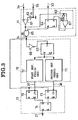
- the present invention is believed to be best embodied in the flyback d.c.-to-d.c. converter, known also as switching regulator, shown in its entirety in FIG. 1.
- the converter has a pair of input terminals 1 a and 1 b , with a d.c. power supply 1 shown connected therebetween, and a pair of output terminals 20 a and 20 b with a load 20 to be powered shown connected therebetween.
- a d.c. power supply 1 shown connected therebetween
- output terminals 20 a and 20 b with a load 20 to be powered shown connected therebetween.
- the primary components of the converter 1 are:
- the three windings 15-17 of the transformer 2 have polarities indicated by the dots in FIG. 1. Thus is energy stored on the transformer 2 during the conducting periods of the switch 3, and released during its nonconducting periods.
- the FET switch 3 has a drain connected to the input terminal 1 a via the transformer primary 15, a source connected to the second input terminal 1 b , which is grounded, and a gate connected to the switch control circuit 7 via the switch driver circuit 8.
- the rectifying and smoothing circuit 5 is shown as a combination of a rectifying diode 18 and a smoothing capacitor 19.
- the smoothing capacitor 19 is connected in parallel with the transformer secondary 16 via the rectifying diode 18.
- the rectifying diode 18 is so oriented with respect to the transformer windings 15 and 16 as to be conductive during the nonconducting periods of the switch 3.
- the smoothing capacitor 19 is also connected between the pair of output terminals 20 a and 20 b .
- the output voltage detector circuit 6 includes two voltage-dividing resistors 21 and 22 connected in series with each other between the pair of output terminals 20 a and 20 b for detecting the converter output voltage V o .
- the junction between these resistors 21 and 22 is connected to one input of a differential amplifier 23, the other input of which is connected to a reference voltage source 24.
- a light-emitting diode or LED 25 provides an optical output having intensity proportional to the converter output voltage V o .
- the switch control circuit 7 includes a phototransistor 47 to be irradiated by the LED 25 of the output voltage detector circuit 6, for providing a voltage proportional to the converter output voltage V o .
- the converter output voltage is utilized for modulating the durations of the switching pulses to be applied to the switch 3.
- the switch control circuit 7 has an input connected to the load magnitude discriminator circuit 13 by way of a line 27. Inputting this load magnitude discriminator circuit output, which is indicative of whether the converter is loaded normally or lightly, the switch control circuit 7 makes on-off control of the switch 3 in either of two prescribed different modes suiting the load magnitude.
- the supply terminal 31 of the switch control circuit 7 is connected as aforesaid to the rectifying and smoothing circuit 9 and, via the resistor 10, to the converter input terminal 1 a .
- the rectifying and smoothing circuit 9 comprises a diode 32 and a capacitor 33 connected to the transformer tertiary 17.
- the output of the switch control circuit 7 is connected by way of a line 29 to the switch driver circuit 8 and thence to the switch 3 and, by way of a line 30, to the flyback period determination circuit 11.
- the switch control circuit 7 is shown in detail in FIG. 2, to which reference will be had presently.
- the flyback period determination circuit 11 is intended for finding the aforesaid flyback period, or the duration of the flyback voltage which develops when the energy that has been stored on the transformer 2 during each conducting period of the switch 3 is released upon subsequent nonconduction of the switch. To this end the flyback period determination circuit 11 is connected to the opposite extremities of the transformer tertiary 17 by way of lines 34 and 35. More will be said about the flyback period determination circuit 11 with reference to FIG. 3.
- the reference period generator circuit 12 Connected to the output line 36 of the flyback period determination circuit 11, the reference period generator circuit 12 generates signals indicative of two reference periods of time from the beginning of each flyback period, for delivery to the load magnitude discriminator circuit 13 by way of lines 37 and 37.
- the reference period generator circuit 12 is also shown in detail in FIG. 3.
- the load magnitude discriminator circuit 13 relies on the outputs from the flyback period determination circuit 11 and the reference period generator circuit 12 for judgment of whether the power demand of the load 20 is normal or less. The results of such judgment are fed over the line 27 to the switch control circuit 7. This switch control circuit will then respond by driving the switch 3 at a relatively high switching frequency if the converter proves normally loaded, and at a lower switching frequency if otherwise.
- the load magnitude discriminator circuit 13 is also shown in detail in FIG. 3.
- the switch control circuit 7 broadly comprises:
- the voltage feedback circuit 40 includes a resistor 46 in addition to the aforesaid phototransistor 47.
- the phototransistor 47 has a collector connected to the supply terminal 31, and an emitter grounded via the resistor 46. There is thus obtained at the junction 48 between resistor 46 and phototransistor 47 a potential proportional to the converter output voltage V o .
- the VCO 42 generates clock pulses at a relatively high frequency, widely accepted in the art, of 100 kHz when the power requirement of the load 20 is normal and at a substantively less frequency of, say, 20 kHz when the power requirement is less.
- the mode selector circuit 44 is connected to the VCO 42 for changing its output frequency between these two values. Included are a first power supply 50 connected to the VCO 42 via a first on-off switch 49, and a second power supply 52 also connected to the VCO via a second on-off switch 51. Both switches 49 and 51 have their control inputs connected to the output line 27 of the load magnitude discriminator circuit 13, the first switch 49 via an inverter 53, and the second switch 51 directly.
- the first switch 49 is closed when the load magnitude discriminator circuit output is low, indicating normal loading
- the second switch 51 is closed when the load magnitude discriminator circuit output is high, indicating light loading.
- the VCO 42 puts out clock pulses at 100 kHz upon closure of the first switch 49, and at 20 kHz upon closure of the second switch 51.
- the VCO 42 delivers the clock pulses to the sawtooth generator 43 at either of the two predetermined frequencies.
- the resulting sawtooth output from the generator 43 is of the same frequency as that of the incoming clock pulses.
- the comparator 41 has a negative input connected to the junction 48 of the voltage feedback circuit 40, and a positive input to the sawtooth generator circuit 43. Thus the comparator 41 puts out the switching pulses V G , shown at (C) in FIG. 4, when the sawtooth voltage is higher than the output voltage of the feedback circuit 40.
- the comparator 41 has its output connected to the gate of the FET switch 3, FIG. 1, via the switch driver circuit 8, so that this switch is turned on and off by the switching pulses V G .
- the voltage regulator circuit 45 is connected to the supply terminal 31 of the switch control circuit 7. Regulating the incoming supply voltage, the voltage regulator circuit 45 powers the necessary components of the switch control circuit 7.
- the specific connections of the voltage regulator circuit 45 to the other parts are not shown because of their impertinence to the invention.
- the switching pulses V G issuing from the switch control circuit 7 as at (C) in this figure have two different periods T 1 and T 2 , T 1 being less than T 2 , depending upon whether the converter is under normal or light load.
- the switching pulses V G have the first period T 1 , which corresponds to the 100 kHz output frequency of the VCO 42, when the output RSFF 74 from the load magnitude discriminator circuit 13 is low, indicating normal loading, as before t 5 and after t 21 as at (K) in FIG. 4.
- the switching pulses V G have the second period T 2 , which corresponds to the 20 kHz output frequency of the VCO 42, when the output RSFF 74 from the load magnitude discriminator circuit 13 is high, indicating light loading, as from t 5 to t 21 as at (K) in FIG. 4. It is also to be noted in connection with FIG. 4 that the switching pulses V G are indefinite in period during the brief transient periods from normal to light loading and the other way around.
- the flyback period determination circuit 11 includes a comparator 61 having a positive input connected to one extremity of the transformer tertiary 17, FIG. 1, by way of a line 34, and a negative input connected to a reference voltage source 62.
- the reference voltage V R from the source 62 is intermediate the maximum and the minimum instantaneous value of the voltage V 3 , inclusive of flyback voltage, across the transformer tertiary 17.
- the comparator 61 will put out pulses during the flyback periods, as from t 3 to t 4 , and from t 7 to t 8 , and during the ensuing ringing periods, as at (C) in FIG. 5.
- a pulse trailing edge detector circuit 63 another component of the flyback period determination circuit 11, comprises a NOT circuit 66 and a NOR gate 67.
- the NOR gate 67 has one input connected to the comparator 61 via the NOT circuit 66, and another input connected directly to the comparator 61.
- the NOT circuit 66 puts out a phase inversion of the input with delay, as at (D) in FIG. 5.
- the NOR gate 67 inputs both this delayed inversion of the comparator output and the original output from the comparator and, as a results, puts out a series of short-duration pulses, as from t 4 to t 5 , from t 4' to t 5' , and from t 8 to t 9 as at (E) in FIG. 5.
- the leading edges of these NOR gate output pulses are in synchronism with the trailing edges of the output pulses of the comparator 61.
- Still another component of the flyback period determination circuit 11 is an RS flip-flop 64 having a set input S connected by way of the line 30 to the output line 29, FIG. 1, of the switch control circuit 7, and a reset input R connected to the NOR gate 67.
- the resulting Q output from the flip-flop 64 is as depicted at (F) in FIG. 5, going low as from t 4 to t 5 , and from t 8 to t 11 .
- flyback period determination circuit 11 Also included in the flyback period determination circuit 11 is an AND gate 65 having one input connected to the comparator 61, and another input to the flip-flop 64.
- the AND gate 65 provides what may be called a flyback period signal V f indicative of the flyback period T f .
- flyback period is meant only the period during which the energy that has been stored on the transformer 2 during each conducting period of the switch 3 is being released continuously in the course of the ensuing nonconducting period of the switch.
- the terms is therefore exclusive of the ringing periods such as from t 8 to t 9 and from t 13 to t 15 in FIG. 4 and from t 8 to t 10 in FIG. 5.
- the ringing is due to the inductance of the transformer 2 and the stray capacitances of the transformer and the switch 3.
- the reference period generator circuit 12 includes a T flip-flop 69 having an inverting trigger input T connected via a NOT circuit 68 to the output 36 of the flyback period determination circuit 11 for inputting the flyback period signal V f . Therefore, triggered by the leading edges of the pulses contained in the flyback period signal V f , as at t 3 , t 7' , t 11 , t 16 , t 19 and t 24 at (E) in FIG. 4 , the flip-flop 69 will put out pulses as at t 3 , t 11 and t 19 at (F) in FIG. 4.
- This flip-flop 69 is intended for positive detection of the starting moments of the flyback voltage no matter how brief it may be in duration.
- the flip-flop 69 has its Q output connected to both first 70 and second 71 reference period generators. These generators 70 and 71 are both timers, putting out pulses having durations indicative of a first T A and a second T B reference period, as at (G) and (H) in FIG. 4, in response to the rises, as at t 3 , t 11 and t 19 , of the FIG. 4 (F) output pulses of the flip-flop 69.
- the first reference period T A represented by the t 3 - t 5 , t 11 - t 12 and t 19 - t 20 periods at (G) in FIG. 4, is set equal to the flyback period at the minimum of normal loading on the converter.
- the second reference period T B is set longer than the first T A .
- the reference periods T A and T B are so determined that the load magnitude on the converter is judged hysteretically on the basis of the flyback period T f .
- the difference in time between the two reference periods T A and T B can be arbitrary, but for the best results it may be from 0.1 to 10.0 microseconds or so.
- the reference period generators 70 and 71 each produce a pulse of the T A or T B duration for every two on-off cycles of the switch 3. This is not an absolute requirement: Triggered instead by the AND gate 65 of the flyback period determination circuit 11, the reference period generators 70 and 71 may be made each to generate one reference period pulse for each on-off cycle of the switch 3.
- the load magnitude discriminator circuit 13 shown also in FIG. 3, is designed to determine whether the converter is loaded normally or lightly, from comparison of the flyback period T f and the reference periods T A and T B . It comprises two D flip-flops 72 and 73 and one RS flip-flop 74. Both D flip-flops 72 and 73 have their data inputs D connected to the output 36 of the flyback period determination circuit 11.
- the first D flip-flop 72 has its phase-inverting clock input CK connected to the first reference period generator 70 of the reference period generator circuit 12, and the second D flop-flop 73 has its phase-inverting clock input CK connected to the second reference period generator 71.
- the first D flip-flop 72 takes in the flyback period signal V f , at (E) in FIG. 4, at the trailing edges of the output pulses of the first reference period generator 70, as at t 5 , t 12 , and t 20 at (G) in FIG. 4.
- the flyback period signal V f is low at t 5 , so that the inverting output of the first D flip-flop 72 will go high as at (I) in FIG. 4.
- the flyback period from t 11 to t 13 in FIG. 4 is shown to be longer than the first reference period T A , from t 11 to t 12 , because of a drop in switching frequency in light load mode of operation. Therefore, as indicated at (I) in FIG. 4, the inverting output of the first D flip-flop 72 goes low at t 12 .
- the second D flip-flop 73 of the load magnitude discriminator circuit 13 takes in the flyback period signal V f , at the trailing edges of the output pulses of the second reference period generator 71 of the reference period generator circuit 12, as at t 6 , t 14 and t 21 at (H) in FIG. 4.
- the flyback period signal V f is low at t 6 and t 14 , with the result that the noninverting output of the second D flip-flop 73 remains low as at (J) in FIG. 4.
- the noninverting output of this flip-flop 73 does, however, go high at t 21 because then the flyback period signal V f is high.
- the two D flip-flops 72 and 73 of the load magnitude discriminator circuit 13 are clocked by the trailing edges of the output pulses of the reference period generators 70 and 71, respectively, of the reference period generator circuit 12. These trailing edges of the output pulses of the generators 70 and 71 indicate the lapse of the predefined reference periods T A and T B , respectively, from the moments of appearance of the flyback voltage V f .
- the RS flip-flop 74 the final component of the FIG. 3 load magnitude discriminator circuit 13, has a set input S connected to the inverting output of the first D flip-flop 72, and a reset input R connected to the noninverting output of the second D flip-flop 73.
- the Q output of the RS flip-flop 74 goes high at t 5 , as at (K) in FIG. 4, when the inverting output of the first D flip-flop 72 goes high as at (I) in FIG. 4. Thereafter, when the noninverting output of the second D flip-flop 73 goes high at t 21 , as at (J) in FIG.
- the RS flip-flop 74 will be reset, with the result that its noninverting output goes low at t 21 , as at (k) in FIG. 4.
- the low state of the RS flip-flop 74 both before t 5 and after t 21 in FIG. 4, indicates normal loading on the converter whereas its high state, from t 5 to t 21 , indicates light loading on the converter.
- This output from the RS flip-flop 74 will be hereinafter referred to as the load magnitude discrimination signal.
- the reference period generator circuit 12 and load magnitude discriminator circuit 13 of the illustrated circuit configurations are intended to ascertain the load magnitude hysteretically, as will be explained in more detail hereinbelow.
- the load magnitude were determined solely by the first reference period generator 70 and the first D flip-flop 72.
- the FIG. 4 (I) output from the D flip-flop 72 would be the load magnitude discrimination signal. If, in the case assumed now, the conducting periods of the switch 3 diminished, as from t 1 to t 2 at (C) in FIG. 4, with a gradual decrease in the power requirement of the load, the flyback period T f would become shorter, as from t 3 to t 4 at (E) in FIG. 4.
- the inverting output of the D flip-flop 72 would go high as at t 5 at (I) in FIG. 4, indicating that the converter is loaded lightly.
- the switching frequency would then drop for operation in light load mode, as from 100 kHz to 20 kHz.
- the consequent decrease in the duty ratio of the switch 3 would invite a decrease in the converter output voltage V o .
- the switching pulses V G , FIG. 4 (C) would increase in duration, as from t 9 to t 10 , in comparison with the pulse from t 1 to t 1 , so that the flyback period T f would become longer than the first reference period T A , as from t 11 to t 13 at (E) in FIG. 4.
- the inverting output of the D flip-flop 72 would go low at t 12 , as at (I) in FIG. 4, indicating normal loading when actually the converter is loaded lightly.
- this flip-flop output would be the load magnitude discrimination signal in the absence of the second reference period generator 71, second D flip-flop 73, and RS flip-flop 74.
- the result would be the hunting of the control system, with the normal and light load modes of operation repeating themselves alternately. Such reiteration of the two operating modes would also cause the on-off cycles of the switch 3 to become irregular, as from t 1 to t 4 , and from t 17 to t 22' in FIG. 4, resulting in the production of noise that would be difficult of removal by a noise filter.
- An additional result would be the instability of the converter output voltage V o .
- the RS flip-flop 74 will not respond to the t 12 change, at (I) in FIG. 4, in the output state of the first D flip-flop 72, remaining high as at (k) in the same figure.
- the flyback period T f first becomes shorter than the first reference period T A , as from t 3 to t 4 in FIG. 4, no change will occur in the output from the load magnitude discriminator circuit 13 even if the flyback period subsequently grows longer than the first reference period as a result of switching. Only when the flyback period T f becomes longer than the second reference period T B will a change occur in the result of load discrimination by the RS flip-flop 74, as at t 21 in FIG. 4.
- the FIG. 3 load magnitude discriminator circuit 13 has its output connected as aforesaid to the FIG. 2 switch control circuit 7, or to the mode selector circuit 44 shown included therein.
- the first switch 49 of this mode selector circuit 44 will be opened, and the second switch 51 closed, when the RS flip-flop 74 of the load magnitude discriminator circuit 13 goes high at t 5 as at (K) in FIG. 4.
- the VCO 42 will thus have its output frequency set at 20 kHz, with the result that the comparator 41 puts out switching pulses V G , FIG. 4 (C), with the second period T 2 .
- the RS flip-flop 74 of the load magnitude discriminator circuit 13 goes low at t 21 , as at (K) in FIG.
- the first switch 49 of the mode selector circuit 44 will be closed, and the second switch 51 opened. Thereupon the VCO 42 will have its output frequency switched to 100 kHz, resulting in the production of switching pulses from the comparator 41 with the second period T 1 .
- the LED 25, FIG. 1, of the output voltage detector circuit 6 will glow with intensity proportional to the converter output voltage V o being applied to the load 20, irradiating the phototransistor 47.
- FIG. 2, of the voltage feedback circuit 40 The resistance of this phototransistor 47 will lower when the output voltage V o grows higher than a target range. The lower resistance of the phototransistor will make higher the potential at the junction 48 between the phototransistor and the resistor 46. Receiving this higher potential into its negative input, the comparator 41 will put out switching pulses of shorter durations. The switch 3 will then conduct for shorter periods of time to lower until the output voltage V o drops to the target range. The reversal of such operation will take place when the output voltage V o falls below the target range.
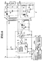
- FIG. 6 An alternate form of d.c.-to-d.c. converter according to the invention is shown in its entirety in FIG. 6.
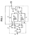
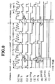
- FIG. 7 is a more detailed illustration of its reference voltage generator circuit 12 and load magnitude discriminator circuit 13, and FIG. 8 a waveform diagram explanatory of its operation.
- FIGS. 1 and 6 A comparison of FIGS. 1 and 6 will reveal that this FIG. 6 converter differs from that of FIG. 1 in having no flyback period determination circuit 11; instead, the switch control circuit 7 is connected directly to the load magnitude discriminator circuit 13 by way of a line 30 a besides being connected to the reference period generator circuit 12 by way of the line 30.
- the FIG. 6 converter is akin to that of FIG. 1 in all the other details of construction.
- the reference voltage generator circuit 12 and load magnitude discriminator circuit 13 are identical in construction with those shown in FIG. 3; only, the NOT circuit 68 and the data inputs D of the D flip-flops 72 and 73 are connected to the switch control circuit 7 by way of the line 30 a .
- This line is intended for delivery of the switching pulses V G to the noted circuit elements 68, 72 and 73 in order to enable the same to know the conducting periods T on , at (C) in FIG. 8, of the switch 3.
- the T flip-flop 69 will put out a series of pulses TFF 69 , FIG. 8 (D), in response to the switching pulses V G , FIG. 8 (C), each having a duration T on .
- Each output pulse TFF 69 of the flip-flop 69 rises with the appearance of every other switching pulse V G .
- the reference period generators 70 and 71 will provide pulses shown at (E) and (F) in FIG. 8, each rising with one flip-flop output pulse and lasting the preassigned reference period T A or T B , for delivery to the load magnitude discriminator circuit 13.
- the D flip-flops 72 and 73 of the load magnitude discriminator circuit 13 will take in the switching pulse signal V G .
- the resulting outputs from these flip-flops 72 and 73 are as shown at (G) and (H) in FIG. 8.
- the flip-flops 72 and 73 functions to determine whether each conducting period T on of the switch 3 is shorter or longer than the two preassigned periods T A and T B .
- the RS flip-flop 74 is set and reset by the leading edges of the FIG. 8 (G) and (H) output pulses of the D flip-flops 72 and 73, respectively, and provides the output seen at (I) in FIG. 8.
- the conducting periods T on , at (C) in FIG. 8, of the switch 3 are in proportion with the flyback period T f , at (E) in FIG. 4. Whether the converter is loaded normally or lightly is therefore ascertainable from a comparison of the switch conducting periods T on and the reference periods T A and T B as in the foregoing.
- the switch control circuit 7 of the FIG. 1 converter is modifiable as indicated at 7 a in FIG. 9.
- the modified switch control circuit 7 a differs from its FIG. 2 counterpart 7 in not having the second switch 51 and second voltage source 52 possessed by the latter but in having, instead, an intermittent switch driver circuit 80.
- the intermittent switch driver circuit 80 Connected between the load magnitude discriminator circuit 13, shown in detail in FIG. 3, and the switch 49, the intermittent switch driver circuit 80 turns this switch on at prescribed time intervals for intermittent converter operation under light load.
- the intermittent switch driver circuit 80 provides the light-load mode signal shown at (C) in FIG. 10.
- the light-load mode signal stays high as long as the load magnitude discrimination signal is low, indicating normal loading, as before t 1 and after t 5 .
- the light-load mode signal takes the form of a series of discrete pulses each having a duration longer than the period T 1 of the switching pulses, FIG. 10 (A), applied to the switch 3.
- the durations of the output pulses, as well as the spacings therebetween, of the intermittent switch drive circuit 80 during light-load operation are each shown to be three times longer than the switching pulse period T 1 in this particular embodiment of the invention. These pulses are applied to the control input of the switch 49 for closing the same at regular intervals.
- the VCO 42 Powered intermittently by the power supply 50 when the converter is under light load, the VCO 42 will generate pulses as from t 2 to t 3 and from t 4 to t 5 as at (D) in FIG. 10.
- the average number of switchings per unit length of time during the t 1 - t 5 light-load operation of FIG. 10 is therefore less than that during the pre- t 1 and post- t 5 normal-mode operation, with consequent reduction in switching loss.
- the d.c.-to-d.c. converter of FIG. 11 features another modified switch control circuit 7 b , shown in detail in FIG. 12, and a resistor 4 connected between the switch 3 and the grounded supply terminal 1 b for detection of the current flowing through the switch.
- the junction between switch 3 and resistor 4 is connected by way of a line 25 to the second modified control circuit 7 b . All the other details of construction are as previously set forth in connection with the FIG. 1 converter.
- the second modified switch control circuit 7 b is designed for converter operation both in normal load mode, in which the switching frequency rises in inverse proportion to the load, as in the familiar ringing choke converter, and in light load mode in which the switching frequency is less than in normal load mode.
- the switch control circuit 7 b comprises a comparator 81, an RS flip-flop 82, a NOR gate 83, a NOT circuit 84 and an amplifier circuit 85, in addition to the various other circuit elements that exist in the FIG. 2 switch control circuit 7 and that therefore are identified by the same reference numerals.
- the comparator 81 has its positive input connected by way of the line 26 to the junction between switch 3 and resistor 4, in order to be supplied with the switch current signal having a voltage V a proportional to the magnitude of the current flowing through the switch.
- the negative input of the comparator 81 is connected to the junction 48 between resistor 46 and phototransistor 47.
- the resistor 46 has one extremity connected to the supply terminal 31, and the other extremity grounded via the phototransistor 47.
- This phototransistor is optically coupled as aforesaid to the LED 25, FIG. 11, of the output voltage detector circuit 6.
- the junction 48 is additionally connected to the amplifier circuit 85.
- the voltage feedback signal having a voltage V b which represents the division of the supply voltage by the resistor 46 and phototransistor 47.
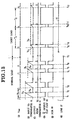
- the voltage V b is in inverse proportion to the converter output voltage V o . Comparing the switch current signal V a and the voltage feedback signal V b as at (B) in FIG. 13, the comparator 81 provides the output V c as at (C) in the same figure.
- the VCO 42 is connected to the amplifier circuit 85 via the first switch 49 and to the power supply 52 via the second switch 51. As in the FIG. 2 switch control circuit 7, the switches 49 and 51 are alternately turned on and off by the load magnitude discrimination signal supplied from the load magnitude discriminator circuit 13, FIG. 11, over the line 27. Therefore, in normal load mode, the VCO 42 will generate the pulses V osc of the variable period T 1 , as from t 1 to t 7 at (A) in FIG. 13, in response to the output from the amplifier circuit 85. In light load mode, on the other hand, the VCO 42 will respond to the supply voltage from the source 52, generating the pulses of the constant period T 2 ,as from t 7 to t 12 at (A) in FIG. 13. These output pulses of the VCO 42 are applied both to the RS flip-flop 82 via the NOT circuit 84 and directly to the NOR gate 83.
- the RS flip-flop 82 has a set input S connected to the VCO 42 via the NOT circuit 84, a reset input R connected to the comparator 81, and an inverting output Q connected to the NOR gate 83.
- This NOR gate 83 has its output connected by way of the line 29 to the switch driver circuit 8, FIG. 11.
- the flip-flop 82 provides the signal seen at (D) in FIG. 13, and the NOR gate 83 the switching pulses seen at (E) in the same figure.
- the first switch 49 will be on, and the second switch 51 off, when the load magnitude discrimination signal on the line 27 is low, indicating normal loading, as from t 1 to t 7 in FIG. 13.
- the VCO 42 will then put out clock pulses V osc , as at (A) in FIG. 13, with a repetition frequency proportional to the output from the amplifier circuit 85.
- the flip-flop 82 Having the set input S connected to the VCO 42 via the NOT circuit 84, the flip-flop 82 will be triggered by the trailing edges of the FIG. 13 (A) output pulses of the VCO 42.
- the flip-flop 82 will therefore be set as at t 1 , t 4 and t 6 in FIG. 13, with its inverting output going low as at (D) in the same figure.
- the magnitude of the voltage feedback signal V b is in proportion to the power consumption of the load 20, and so are the length of time during which the flip-flop 82 stays set, and the duration of each output pulse of the NOR gate.
- the on-off frequency of the switch 3 is in inverse proportion to the power consumption of the load 20.
- the first switch 49 of the FIG. 12 switch control circuit 7 b will be off, and the second switch 51 on, when the load magnitude discrimination signal on the output line 27 of the load magnitude discriminator circuit 13 is high, indicating light loading as from t 8 to t 12 in FIG. 13.
- the VCO 42 Powered by the constant voltage from the source 52, the VCO 42 will generate pulses at a constant repetition frequency as at (A) in FIG. 13.
- the period T 2 of these constant frequency pulses in light load mode is less than the maximum period T 1 of those in normal load mode before t 7 .
- Converter operation in light load mode is analogous with that in normal load mode except that the switch 3 is driven with a constant on-off period T 2 .
- FIG. 11 converter 11 relies on the flyback voltage for finding whether it is under normal or light load, and switchings per unit length of time are reduced in light load mode for higher efficiency.
- the judgment of load magnitude by the load magnitude discriminator circuit 13 is done hysteretically as in the FIG. 1 converter.
- the FIG. 11 converter is further modifiable to ascertain load magnitude by comparison of the durations of the switching pulses V G at (E) in FIG. 13 and the two reference periods of time T A and T B seen in FIG. 8, as in the second disclosed embodiment of the invention.
- FIG. 14 illustrates another modification 7 c of the FIG. 12 switch control circuit 7 b of the FIG. 11 converter.
- the modified switch control circuit 7 c differs from the circuit 7 b in having an intermittent switch driver circuit 90 and a third switch 91 in addition to all the circuit elements included in the FIG. 12 switch control circuit 7 b .
- the intermittent switch driver circuit 90 is itself similar to that shown at 80 in FIG. 9, putting out the pulses of FIG. 10 (C) at constant intervals when the load magnitude discrimination signal on the line 27 indicates light loading, and hence closing the third switch intermittently.
- the third switch 91 is connected between VCO 42 and second switch 51. Closed intermittently in light load mode, the third switch 91 causes the VCO 42 to be powered intermittently from the power supply 52.
- the FIG. 14 switch control circuit 7 c offers the same advantages as does its FIG. 9 counterpart 7 a .
- the switch control circuit 7 c lends itself to use in substitution for the switch control circuit 7 of the FIG. 6 converter.
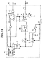
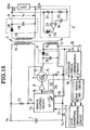
- the d.c.-to-d.c. converter of FIG. 15 incorporates a further modified switch control circuit 7 d , shown in detail in FIG. 16, and is akin to that of FIG. 11 in other respects.
- the switch control circuit 7 d relies on the flyback voltage developing across the transformer tertiary 17 for determination of the ending moments of the switch nonconducting periods during operation in normal load mode, so that the transformer tertiary is shown connected to the switch control circuit 7 d by way of the line 28 in FIG. 15.
- the modified switch control circuit 7 d comprises a switch conduction terminating circuit 100, a switch nonconduction terminating circuit 101, and an RS flip-flop 102, in addition to the voltage regulator circuit 45 as in the FIGS. 2 and 12 switch control circuits 7 and 7 b .
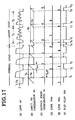
- the switch conduction terminating circuit 100 is similar in construction to its counterpart of the FIG. 12 switch control circuit 7 b , comprising the resistor 46, phototransistor 47, and comparator 81. Comparing the switch current signal V a on the line 26 and the voltage feedback signal V b from the junction 48, as at (B) in FIG. 17, the comparator 81 puts out a pulse, at (C) in FIG.
- the switch nonconduction terminating circuit 101 comprises a circuit 104 for termination of switch nonconducting periods in normal load mode, an oscillator 105 for termination of switch nonconducting periods in light load mode, two mode select switches 49 and 51, and a NOT circuit 53.
- the normal load mode switch nonconduction terminating circuit 101 has an input connected to the transformer tertiary 17, FIG. 15, by way of the line 28 for detection of the voltage across the same, and another input connected to the comparator 81.
- the circuit 101 In response to each output pulse of the comparator 81, the circuit 101 ascertains the moment the voltage V 3 across the transformer tertiary 17 first drops to a minimum after the appearance of each FIG. 17 (C) comparator output pulse.
- the resulting output pulses on the line 104 a of the circuit 104 are indicated at (D) in FIG. 17.
- the transformer tertiary voltage V 3 minimizes when the voltage V DS across the switch minimizes after the duration of the flyback voltage.
- the normal load mode switch nonconduction terminating circuit 104 has its output line 104 a connected to the set input S of the flip-flop 102 via the first mode select switch 49.
- This switch 49 as aforesaid is under the control of the load magnitude discrimination signal on the line 27 via the NOT circuit 53.
- the flip-flop 102 is therefore set by each FIG. 17 (D) output pulse of the circuit 104, as at t 2 . Having its Q output connected directly to the switch 3 via the driver circuit 8, the flip-flop 102 provides the switching pulses V G for on-off control of the switch 3.
- the operation of this converter in normal load mode is similar to that of the known ringing choke comparator, with both conducting periods T on and nonconducting periods T off of the switch 3 changing with power consumption by the load 20.
- the oscillator 105 puts out pulses on its output line 105 a , as at (E) in FIG. 17, with a repetition frequency of, typically, 20 kHz, which is less than the minimum switching frequency of the switch 3 in normal load mode.
- the oscillator output line 105 a is connected via the second mode select switch 51 to the set input S of the flip-flop 102.
- This second mode select switch 51 is closed in light load mode, as after t 4 in FIG. 17, so that the flip-flop 102 will be set as at t 5 , t 7 and t 9 by the FIG. 17 (E) output pulses of the oscillator 105 and reset at t 6 , t 8 and t 10 by the FIG. 17 (C) output pulses of the comparator 81.
- the dedicated oscillator 105 for termination of the nonconducting periods of the switch 3 is not an absolute necessity; instead, an oscillator included in the normal load mode switch nonconduction terminating circuit 104 may be utilized for obtaining the FIG. 17 (E) pulses.
- the switch nonconduction terminating circuit 101 can be of any design as long as it can provide a first series of pulses for terminating the conducting periods of the switch 3 being driven in normal load mode as in the ringing choke converter, and a second series of pulses for terminating the conducting periods of the switch being driven in light load mode at a lower switching frequency than in normal load mode.
- the FIG. 15 converter discriminates between normal and light load modes just like the FIG. 1 converter, so that it gains the same advantages therewith. Switching loss is further reduced in this embodiment, moreover, because the switch is turned on when the voltage across the same is practically zero. When the voltage across the switch becomes zero is not detected in light load mode in this particular embodiment of the invention. It is, of course, modifiable to turn on the switch at no voltage. It is also possible to use this switch control circuit 7 d in place of its FIG. 6 counterpart 7.
- FIG. 18 is shown a still further modified switch control circuit 7 e , suitable for use in the FIG. 15 converter in substitution for the FIG. 16 switch control circuit 7 d .
- the switch control circuit 7 e differs from its FIG. 16 counterpart 7 d in having an intermittent switch driver circuit 110 and a switch 111 in addition to all the other parts and components existing in the latter.
- the switch 111 is connected between the switch 51 and the set input S of the RS flip-flop 102, and the intermittent switch driver circuit 110 between the output line 27 of the load magnitude discriminator circuit 13, FIG. 15 , and the control input of the switch 111.
- the intermittent switch driver circuit 110 causes the switch 3 to be driven on and off at regular intervals in light load mode in response to the load magnitude discrimination signal fed over the line 27.
- the mean number of switchings per unit length of time is thus reduced in light load mode.
- This switch control circuit 7 e could be used in the FIG. 6 converter in place of its switch control circuit 7.
- the final embodiment of the invention differs from that of FIG. 1 in having a reactor or inductor 2 a in place of the transformer 2, and having the rectifying and smoothing circuit 5 connected in parallel with the switch 3.
- the reactor 2 a has the windings 15 and 17 but no equivalent to the secondary transformer 16 of the FIG. 1 transformer 2.
- the other details of construction are as previously set forth with reference to FIGS. 1-3.
- the rectifying diode 18 of the rectifying and smoothing circuit 5 will be reverse-biased during the conducting periods of the switch 3, thereby causing energy to be stored on the reactor 2 a .
- the rectifying diode 18 will cause the reactor to release the energy.
- the capacitor 19 will then be charged by the resultant of the voltage across the power supply 1 and that across the reactor winding 15. In short this converter will function as step-up switching regulator.
- This type of reactor could be used in all the other embodiments of the invention disclosed herein.
Landscapes
- Engineering & Computer Science (AREA)
- Power Engineering (AREA)
- Dc-Dc Converters (AREA)
Abstract
Description
Claims (16)
- A d.c.-to-d.c. converter to be connected between a d.c. power supply and a load to be powered, comprising a pair of input terminals (1a and 1b) to be connected to a d.c. power supply (1) for inputting a d.c. voltage, a switch (3) connected between the pair of input terminals in order to be repeatedly turned on and off by a series of switching pulses (VG ) for switching the d.c. power supply, inductance means (2 or 2a) connected in series with the switch, a rectifying and smoothing circuit (5) connected to the inductance means for providing an output voltage (Vo ) to be applied to the load (20), and an output voltage detector circuit (6) for detecting the output voltage (Vo ), characterized in that a switch control circuit (7, 7a, 7b, 7c, 7d or 7e) is connected between the output voltage detector circuit (6) and the switch (3) for delivering to the latter the series of switching pulses (VG ) which are modulated according to the converter output voltage (Vo ) in order to keep the converter output voltage constant, that a flyback period determination circuit (11) is connected to the inductance means (2 o 2a) for providing a flyback period signal (Vf ) indicative of a flyback period (Tf ) during which a flyback voltage exists across the inductance means after the switch has been turned off each time, and that a load magnitude discriminator circuit (13) has an input connected to the flyback period determination circuit (11), and another input connected to a reference period generator circuit (12) which provides at least one reference period of time (TA , TB ), in order to provide a load magnitude discrimination signal indicative of whether the converter is under normal or light load by comparing the flyback period (Tf ) and the reference period (TA , TB ), the load magnitude discrimination signal being delivered to the switch control circuit for causing the same to make on-off control of the switch in either of two different prescribed modes depending upon whether the converter is under normal or light load.
- A d.c.-to-d.c. converter as claimed in claim 1, characterized in that the reference period generator circuit (12) comprises a first reference period generator (70) for providing a signal indicative of a first reference period of time (TA ) following the beginning of each flyback period (Tf ), and a second reference period generator (71) for providing a signal indicative of a second reference period of time (TB ) following the beginning of each flyback period (Tf ), the second reference period being longer than the first reference period.
- A d.c.-to-d.c. converter as claimed in claim 2, characterized in that the load magnitude discriminator circuit (13) comprises first circuit means (72) for comparing each flyback period (Tf ) with the first reference period (TA ), second circuit means (73) for comparing each flyback period (Tf ) with the second reference period (TB ), and third circuit means (74) connected between the first and second circuit means of the load magnitude discriminator circuit (13) and the switch control circuit (7) for supplying to the latter the load magnitude discrimination signal indicative of normal loading when each flyback period (Tf ) is longer than the second reference period (TB ), and of light loading when each flyback period is not longer than the first reference period (TA ).
- A d.c.-to-d.c. converter as claimed in claim 2, characterized in that the load magnitude discriminator circuit (13) comprises a first D flip-flop (72) having a data input connected to the flyback period determination circuit (11) for inputting the flyback period signal (Vf ), and a clock input connected to the first reference period generator (70) of the reference period generator circuit (12) in order to be clocked at the end of the first reference period (TA ), a second D flip-flop (73) having a data input connected to the flyback period determination circuit (11) for inputting the flyback period signal (Vf ), and a clock input connected to the second reference period generator (71) of the reference period generator circuit (12) in order to be clocked at the end of the second reference period (TB ), and an RS flip-flop (74) having a set input connected to the first D flip-flop (72) in order to be thereby triggered when the first D flip-flop is reset, a reset input connected to the second D flip-flop (73) in order to be thereby triggered when the second D flip-flop is set, and an output for providing the load magnitude discrimination signal indicative of normal loading when the RS flip-flop (74) is set, and of light loading when the RS flip-flop is reset.
- A d.c.-to-d.c. converter as claimed in claim 1, characterized in that the switch control circuit (7) comprises first circuit means (49 and 50 with 40-43) for making on-off control of the switch (3) at a first repetition frequency when the load magnitude discrimination signal from the load magnitude discriminator circuit (13) indicates normal loading, and second circuit means (51 and 52 with 40-43) for making on-off control of the switch (3) at a second repetition frequency, which is less than the first repetition frequency, when the load magnitude discrimination signal indicates light loading.
- A d.c.-to-d.c. converter as claimed in claim 1, characterized in that the switch control circuit (7b) comprises first circuit means (49, 81, 85, etc., with 42, 82, 83, etc.) for making on-off control of the switch at a repetition frequency that is in inverse proportion to the load magnitude when the load magnitude discrimination signal from the load magnitude discriminator circuit (13) indicates normal loading, and second circuit means (51 and 52 with 42, 82, 83, etc.) for making on-off control of the switch at a fixed repetition frequency, which is less than a minimum of the repetition frequencies during normal loading, when the load magnitude discrimination signal indicates light loading.
- A d.c.-to-d.c. converter as claimed in claim 1, characterized in that the switch control circuit (7a) comprises first circuit means (50 with 40-43) for making on-off control of the switch at a prescribed repetition frequency when the load magnitude discrimination signal from the load magnitude discriminator circuit (13) indicates normal loading, and second circuit means (49 and 80) for making on-off control of the switch at intervals at the prescribed repetition frequency when the output signal of the load magnitude discriminator circuit indicates light loading.
- A d.c.-to-d.c. converter as claimed in claim 1, characterized in that the switch control circuit (7c and 7e) comprises first circuit means (100, 104 and 102) for making on-off control of the switch at a repetition frequency that is in inverse proportion to the load magnitude when the load magnitude discrimination signal from the load magnitude discriminator circuit (13) indicates normal loading, and second circuit means (42, 51, 52, 90 and 91; or 51, 105, 110 and 111) for making on-off control of the switch at intervals, and at a repetition frequency less than a minimum of the repetition frequencies during normal loading, when the load magnitude discrimination signal indicates light loading.
- A d.c.-to-d.c. converter to be connected between a d.c. power supply and a load to be powered, comprising a pair of input terminals (1a and 1b) to be connected to a d.c. power supply (1) for inputting a d.c. voltage, a switch (3) connected between the pair of input terminals in order to be repeatedly turned on and off by a series of switching pulses (VG ) for switching the d.c. power supply, inductance means (2 or 2a) connected in series with the switch, a rectifying and smoothing circuit (5) connected to the inductance means for providing an output voltage (Vo ) to be applied to the load (20), and an output voltage detector circuit (6) for detecting the output voltage (Vo ), characterized in that a switch control circuit (7, 7a, 7b, 7c, 7d or 7e) is connected between the output voltage detector circuit (6) and the switch (3) for delivering to the latter the series of switching pulses (VG ) which are modulated according to the converter output voltage (Vo ) in order to keep the converter output voltage constant, that a load magnitude discriminator circuit (13) has an input connected to means (30) for ascertaining the conducting periods (Ton ) of the switch (3), and another input connected to a reference period generator circuit (12) which provides at least one reference period of time (TA , TB ), in order to provide a load magnitude discrimination signal indicative of whether the converter is under normal or light load by comparing each conducting period (Ton ) of the switch and the reference period (TA , TB ), the load magnitude discriminator circuit having an output connected to the switch control circuit for causing the same to make on-off control of the switch in either of two different prescribed modes depending upon whether the converter is under normal or light load.
- A d.c.-to-d.c. converter as claimed in claim 9, characterized in that the reference period generator circuit (12) comprises a first reference period generator (70) for providing a signal indicative of a first reference period of time (TA ) following the beginning of each conducting period (Ton ) of the switch (3), and a second reference period generator (71) for providing a signal indicative of a second reference period of time (TB ) following the beginning of each conducting period (Ton ) of the switch, the second reference period being longer than the first reference period.
- A d.c.-to-d.c. converter as claimed in claim 10, characterized in that the load magnitude discriminator circuit (13) comprises first circuit means (72) for comparing each conducting period (Ton ) of the switch with the first reference period (TA ), second circuit means (73) for comparing each conducting period (Ton ) of the switch with the second reference period (TB ), and third circuit means (74) connected between the first and second circuit means of the load magnitude discriminator circuit (13) and the switch control circuit (7) for supplying to the latter the load magnitude discrimination signal indicative of normal loading when each switch conducting period (Ton ) is longer than the second reference period (TB ), and of light loading when each switch conducting period is not longer than the first reference period (TA ).
- A d.c.-to-d.c. converter as claimed in claim 10, characterized in that the load magnitude discriminator circuit (13) comprises a first D flip-flop (72) having a data input connected to the ascertaining means (30) for inputting the switching pulses (VG ), and a clock input connected to the first reference period generator (70) of the reference period generator circuit (12) in order to be clocked at the end of the first reference period (TA ), a second D flip-flop (73) having a data input connected to the ascertaining means (30) for inputting the switching pulses (VG ), and a clock input connected to the second reference period generator (71) of the reference period generator circuit (12) in order to be clocked at the end of the second reference period (TB ), and an RS flip-flop (74) having a set input connected to the first D flip-flop (72) in order to be thereby triggered when the first D flip-flop is reset, a reset input connected to the second D flip-flop (73) in order to be thereby triggered when the second D flip-flop is set, and an output for providing the load magnitude discrimination signal indicative of normal loading when the RS flip-flop (74) is set, and light loading when the RS flip-flop is reset.
- A d.c.-to-d.c. converter as claimed in claim 9, characterized in that the switch control circuit (7) comprises first circuit means (49 and 50 with 40-43) for making on-off control of the switch (3) at a first repetition frequency when the load magnitude discrimination signal from the load magnitude discriminator circuit (13) indicates normal loading, and second circuit means (51 and 52 with 40-43) for making on-off control of the switch (3) at a second repetition frequency, which is less than the first repetition frequency, when the load magnitude discrimination signal indicates light loading.
- A d.c.-to-d.c. converter as claimed in claim 10, characterized in that the switch control circuit (7b) comprises first circuit means (49, 81, 85, etc., with 42, 82, 83, etc.) for making on-off control of the switch at a repetition frequency that is in inverse proportion to the load magnitude when the load magnitude discrimination signal from the load magnitude discriminator circuit (13) indicates normal loading, and second circuit means (51 and 52 with 42, 82, 83, etc.) for making on-off control of the switch at a fixed repetition frequency, which is less than a minimum of the repetition frequencies during normal loading, when the load magnitude discrimination signal indicates light loading.
- A d.c.-to-d.c. converter as claimed in claim 10, characterized in that the switch control circuit (7a) comprises first circuit means (50 with 40-43) for making on-off control of the switch at a prescribed repetition frequency when the load magnitude discrimination signal from the load magnitude discriminator circuit (13) indicates normal loading, and second circuit means (49 and 80) for making on-off control of the switch at intervals at the prescribed repetition frequency when the output signal of the load magnitude discriminator circuit indicates light loading.
- A d.c.-to-d.c. converter as claimed in claim 10, characterized in that the switch control circuit (7c and 7e) comprises first circuit means (100, 104 and 102) for making on-off control of the switch at a repetition frequency that is in inverse proportion to the load magnitude when the load magnitude discrimination signal from the load magnitude discriminator circuit (13) indicates normal loading, and second circuit means (42, 51, 52, 90 and 91; or 51, 105, 110 and 111) for making on-off control of the switch at intervals, and at a repetition frequency less than a minimum of the repetition frequencies during normal loading, when the load magnitude discrimination signal indicates light loading.
Applications Claiming Priority (2)
| Application Number | Priority Date | Filing Date | Title |
|---|---|---|---|
| JP2000369199 | 2000-12-04 | ||
| JP2000369199A JP3371962B2 (en) | 2000-12-04 | 2000-12-04 | DC-DC converter |
Publications (3)
| Publication Number | Publication Date |
|---|---|
| EP1213823A2 true EP1213823A2 (en) | 2002-06-12 |
| EP1213823A3 EP1213823A3 (en) | 2002-11-13 |
| EP1213823B1 EP1213823B1 (en) | 2004-02-11 |
Family
ID=18839273
Family Applications (1)
| Application Number | Title | Priority Date | Filing Date |
|---|---|---|---|
| EP01128657A Expired - Lifetime EP1213823B1 (en) | 2000-12-04 | 2001-11-30 | DC-to-DC converter |
Country Status (5)
| Country | Link |
|---|---|
| US (1) | US6515876B2 (en) |
| EP (1) | EP1213823B1 (en) |
| JP (1) | JP3371962B2 (en) |
| CN (1) | CN1193486C (en) |
| DE (1) | DE60101991T2 (en) |
Cited By (47)
| Publication number | Priority date | Publication date | Assignee | Title |
|---|---|---|---|---|
| WO2008137654A1 (en) * | 2007-05-02 | 2008-11-13 | Cirrus Logic, Inc. | System and method with inductor flyback detection using switch gate charge characteristic detection |
| US7667408B2 (en) | 2007-03-12 | 2010-02-23 | Cirrus Logic, Inc. | Lighting system with lighting dimmer output mapping |
| US7696913B2 (en) | 2007-05-02 | 2010-04-13 | Cirrus Logic, Inc. | Signal processing system using delta-sigma modulation having an internal stabilizer path with direct output-to-integrator connection |
| US7755525B2 (en) | 2008-01-30 | 2010-07-13 | Cirrus Logic, Inc. | Delta sigma modulator with unavailable output values |
| US7759881B1 (en) | 2008-03-31 | 2010-07-20 | Cirrus Logic, Inc. | LED lighting system with a multiple mode current control dimming strategy |
| EP2224583A1 (en) | 2009-01-30 | 2010-09-01 | Power Integrations, Inc. | Method and apparatus to regulate an output voltage of a power converter at light/no load conditions |
| US7804256B2 (en) | 2007-03-12 | 2010-09-28 | Cirrus Logic, Inc. | Power control system for current regulated light sources |
| US7994863B2 (en) | 2008-12-31 | 2011-08-09 | Cirrus Logic, Inc. | Electronic system having common mode voltage range enhancement |
| US8018171B1 (en) | 2007-03-12 | 2011-09-13 | Cirrus Logic, Inc. | Multi-function duty cycle modifier |
| US8022683B2 (en) | 2008-01-30 | 2011-09-20 | Cirrus Logic, Inc. | Powering a power supply integrated circuit with sense current |
| US8076920B1 (en) | 2007-03-12 | 2011-12-13 | Cirrus Logic, Inc. | Switching power converter and control system |
| US8102127B2 (en) | 2007-06-24 | 2012-01-24 | Cirrus Logic, Inc. | Hybrid gas discharge lamp-LED lighting system |
| US8179110B2 (en) | 2008-09-30 | 2012-05-15 | Cirrus Logic Inc. | Adjustable constant current source with continuous conduction mode (“CCM”) and discontinuous conduction mode (“DCM”) operation |
| US8212491B2 (en) | 2008-07-25 | 2012-07-03 | Cirrus Logic, Inc. | Switching power converter control with triac-based leading edge dimmer compatibility |
| US8248145B2 (en) | 2009-06-30 | 2012-08-21 | Cirrus Logic, Inc. | Cascode configured switching using at least one low breakdown voltage internal, integrated circuit switch to control at least one high breakdown voltage external switch |
| US8288954B2 (en) | 2008-12-07 | 2012-10-16 | Cirrus Logic, Inc. | Primary-side based control of secondary-side current for a transformer |
| US8299722B2 (en) | 2008-12-12 | 2012-10-30 | Cirrus Logic, Inc. | Time division light output sensing and brightness adjustment for different spectra of light emitting diodes |
| US8344707B2 (en) | 2008-07-25 | 2013-01-01 | Cirrus Logic, Inc. | Current sensing in a switching power converter |
| US8362838B2 (en) | 2007-01-19 | 2013-01-29 | Cirrus Logic, Inc. | Multi-stage amplifier with multiple sets of fixed and variable voltage rails |
| US8362707B2 (en) | 2008-12-12 | 2013-01-29 | Cirrus Logic, Inc. | Light emitting diode based lighting system with time division ambient light feedback response |
| EP1655826A3 (en) * | 2004-11-05 | 2013-05-29 | Power Integrations, Inc. | Method and apparatus to provide temporary peak power from a switching regulator |
| US8482223B2 (en) | 2009-04-30 | 2013-07-09 | Cirrus Logic, Inc. | Calibration of lamps |
| US8487546B2 (en) | 2008-08-29 | 2013-07-16 | Cirrus Logic, Inc. | LED lighting system with accurate current control |
| US8487591B1 (en) | 2009-12-31 | 2013-07-16 | Cirrus Logic, Inc. | Power control system with power drop out immunity and uncompromised startup time |
| US8576589B2 (en) | 2008-01-30 | 2013-11-05 | Cirrus Logic, Inc. | Switch state controller with a sense current generated operating voltage |
| US8654483B2 (en) | 2009-11-09 | 2014-02-18 | Cirrus Logic, Inc. | Power system having voltage-based monitoring for over current protection |
| WO2013108155A3 (en) * | 2012-01-19 | 2014-03-06 | Koninklijke Philips N.V. | Power supply device |
| US8866452B1 (en) | 2010-08-11 | 2014-10-21 | Cirrus Logic, Inc. | Variable minimum input voltage based switching in an electronic power control system |
| US8912781B2 (en) | 2010-07-30 | 2014-12-16 | Cirrus Logic, Inc. | Integrated circuit switching power supply controller with selectable buck mode operation |
| US8963535B1 (en) | 2009-06-30 | 2015-02-24 | Cirrus Logic, Inc. | Switch controlled current sensing using a hall effect sensor |
| US9024541B2 (en) | 2013-03-07 | 2015-05-05 | Cirrus Logic, Inc. | Utilizing secondary-side conduction time parameters of a switching power converter to provide energy to a load |
| US9155174B2 (en) | 2009-09-30 | 2015-10-06 | Cirrus Logic, Inc. | Phase control dimming compatible lighting systems |
| US9178444B2 (en) | 2011-12-14 | 2015-11-03 | Cirrus Logic, Inc. | Multi-mode flyback control for a switching power converter |
| US9178415B1 (en) | 2009-10-15 | 2015-11-03 | Cirrus Logic, Inc. | Inductor over-current protection using a volt-second value representing an input voltage to a switching power converter |
| US9214862B2 (en) | 2014-04-17 | 2015-12-15 | Philips International, B.V. | Systems and methods for valley switching in a switching power converter |
| US9253833B2 (en) | 2013-05-17 | 2016-02-02 | Cirrus Logic, Inc. | Single pin control of bipolar junction transistor (BJT)-based power stage |
| US9313840B2 (en) | 2011-06-03 | 2016-04-12 | Cirrus Logic, Inc. | Control data determination from primary-side sensing of a secondary-side voltage in a switching power converter |
| US9325236B1 (en) | 2014-11-12 | 2016-04-26 | Koninklijke Philips N.V. | Controlling power factor in a switching power converter operating in discontinuous conduction mode |
| US9351356B2 (en) | 2011-06-03 | 2016-05-24 | Koninklijke Philips N.V. | Primary-side control of a switching power converter with feed forward delay compensation |
| US9496855B2 (en) | 2013-07-29 | 2016-11-15 | Cirrus Logic, Inc. | Two terminal drive of bipolar junction transistor (BJT) of a light emitting diode (LED)-based bulb |
| US9504106B2 (en) | 2013-07-29 | 2016-11-22 | Cirrus Logic, Inc. | Compensating for a reverse recovery time period of a bipolar junction transistor (BJT) in switch-mode operation of a light-emitting diode (LED)-based bulb |
| US9504118B2 (en) | 2015-02-17 | 2016-11-22 | Cirrus Logic, Inc. | Resistance measurement of a resistor in a bipolar junction transistor (BJT)-based power stage |
| US9510401B1 (en) | 2010-08-24 | 2016-11-29 | Cirrus Logic, Inc. | Reduced standby power in an electronic power control system |
| US9520794B2 (en) | 2012-07-25 | 2016-12-13 | Philips Lighting Holding B.V | Acceleration of output energy provision for a load during start-up of a switching power converter |
| US9603206B2 (en) | 2015-02-27 | 2017-03-21 | Cirrus Logic, Inc. | Detection and control mechanism for tail current in a bipolar junction transistor (BJT)-based power stage |
| US9609701B2 (en) | 2015-02-27 | 2017-03-28 | Cirrus Logic, Inc. | Switch-mode drive sensing of reverse recovery in bipolar junction transistor (BJT)-based power converters |
| US9735671B2 (en) | 2013-05-17 | 2017-08-15 | Cirrus Logic, Inc. | Charge pump-based drive circuitry for bipolar junction transistor (BJT)-based power supply |
Families Citing this family (72)
| Publication number | Priority date | Publication date | Assignee | Title |
|---|---|---|---|---|
| FR2827109B1 (en) * | 2001-07-05 | 2003-11-07 | Eastman Kodak Co | METHOD FOR IDENTIFYING SHADOWS IN AN IMAGE AND IMAGE OBTAINED THANKS TO THIS PROCESS |
| JP3494223B2 (en) * | 2001-12-03 | 2004-02-09 | サンケン電気株式会社 | DC-DC converter |
| KR100856900B1 (en) * | 2001-12-21 | 2008-09-05 | 페어차일드코리아반도체 주식회사 | Burst Mode Switching Mode Power Supplies |
| JP4085335B2 (en) * | 2002-08-30 | 2008-05-14 | サンケン電気株式会社 | Switching power supply |
| KR100667468B1 (en) * | 2002-09-04 | 2007-01-10 | 산켄덴키 가부시키가이샤 | DC-DC converter |
| KR100732353B1 (en) * | 2002-12-18 | 2007-06-27 | 페어차일드코리아반도체 주식회사 | Control module circuit in switching power supply with automatic burst mode operation |
| JP4212366B2 (en) * | 2003-01-16 | 2009-01-21 | 新電元工業株式会社 | Switching power supply |
| CN100454205C (en) * | 2003-02-03 | 2009-01-21 | Jam技术有限责任公司 | An Improved Method of Detecting the Output Current of Switching Power Supply |
| CN1303750C (en) * | 2003-03-17 | 2007-03-07 | 华南理工大学 | Soft-switch hidden-arc welding contrarariant power supply with double closed-loop control |
| US7275501B1 (en) * | 2003-07-03 | 2007-10-02 | Laceky William P | System and method using capacitors to power an automatic feeder system |
| US8525469B1 (en) | 2003-07-03 | 2013-09-03 | Battery-Free Outdoors, Llc | System and method using capacitors to power a camera having a motion sensor |
| DE10347193A1 (en) * | 2003-10-10 | 2005-05-12 | Thomson Brandt Gmbh | Switching Power Supply |
| JP2005261112A (en) * | 2004-03-12 | 2005-09-22 | Sanken Electric Co Ltd | Dc-dc converter |
| CN100466438C (en) * | 2004-05-24 | 2009-03-04 | 松下电器产业株式会社 | Switching power supply unit |
| JP3973652B2 (en) * | 2004-05-24 | 2007-09-12 | 松下電器産業株式会社 | Switching power supply |
| JP4400426B2 (en) | 2004-11-19 | 2010-01-20 | サンケン電気株式会社 | Switching power supply |
| WO2006088454A1 (en) * | 2005-02-17 | 2006-08-24 | General Motors Corporation | Method and system for managing processor execution time utilizing variable frequency switching |
| US7265999B2 (en) * | 2005-04-06 | 2007-09-04 | Matsushita Electric Industrial Co., Ltd. | Power supply regulator circuit and semiconductor device |
| US7453709B2 (en) * | 2005-07-08 | 2008-11-18 | Power Integrations, Inc. | Method and apparatus for increasing the power capability of a power supply |
| CN101295872B (en) | 2007-04-28 | 2010-04-14 | 昂宝电子(上海)有限公司 | Systems and methods for providing overcurrent and overpower protection for power converters |
| US20070159143A1 (en) * | 2006-01-11 | 2007-07-12 | Ta-Yung Yang | Switching power converter with transformer arrangement |
| CN101127495B (en) | 2006-08-16 | 2010-04-21 | 昂宝电子(上海)有限公司 | Systems and methods for providing control for switching mode power supplies |
| US7518885B2 (en) | 2006-10-04 | 2009-04-14 | Power Integrations, Inc. | Method and apparatus for a control circuit with multiple operation modes |
| US7911808B2 (en) * | 2007-02-10 | 2011-03-22 | Active-Semi, Inc. | Primary side constant output current controller with highly improved accuracy |
| KR101309293B1 (en) * | 2007-03-28 | 2013-09-16 | 페어차일드코리아반도체 주식회사 | Switching mode power supply and the driving method thereof |
| US7764520B2 (en) * | 2007-04-06 | 2010-07-27 | Power Integrations, Inc. | Method and apparatus for on/off control of a power converter |
| US7869229B2 (en) * | 2007-04-23 | 2011-01-11 | Active-Semi, Inc. | Compensating for cord resistance to maintain constant voltage at the end of a power converter cord |
| CN101340155B (en) * | 2007-07-06 | 2012-05-16 | 立锜科技股份有限公司 | Apparatus and method for improving light load performance of a flyback voltage converter |
| US8031496B2 (en) * | 2007-11-07 | 2011-10-04 | Panasonic Corporation | Driving circuit for power switching device, driving method thereof, and switching power supply apparatus |
| KR20090050318A (en) * | 2007-11-15 | 2009-05-20 | 삼성전자주식회사 | Power converter with automatic switching function in pulse skip mode and control method |
| US7804697B2 (en) | 2007-12-11 | 2010-09-28 | Cirrus Logic, Inc. | History-independent noise-immune modulated transformer-coupled gate control signaling method and apparatus |
| US8008898B2 (en) | 2008-01-30 | 2011-08-30 | Cirrus Logic, Inc. | Switching regulator with boosted auxiliary winding supply |
| US8008902B2 (en) | 2008-06-25 | 2011-08-30 | Cirrus Logic, Inc. | Hysteretic buck converter having dynamic thresholds |
| US8330434B2 (en) | 2008-07-25 | 2012-12-11 | Cirrus Logic, Inc. | Power supply that determines energy consumption and outputs a signal indicative of energy consumption |
| JP2010081686A (en) * | 2008-09-24 | 2010-04-08 | Panasonic Corp | Switching control circuit and switching power supply |
| US8222872B1 (en) | 2008-09-30 | 2012-07-17 | Cirrus Logic, Inc. | Switching power converter with selectable mode auxiliary power supply |
| US7864550B2 (en) * | 2008-11-05 | 2011-01-04 | Bcd Semiconductor Manufacturing Limited | Power adapter with voltage-stabilized compensation |
| JP2010288334A (en) * | 2009-06-09 | 2010-12-24 | Panasonic Corp | Switching power supply device and semiconductor device |
| US8212493B2 (en) | 2009-06-30 | 2012-07-03 | Cirrus Logic, Inc. | Low energy transfer mode for auxiliary power supply operation in a cascaded switching power converter |
| US8198874B2 (en) | 2009-06-30 | 2012-06-12 | Cirrus Logic, Inc. | Switching power converter with current sensing transformer auxiliary power supply |
| GB2475261B (en) * | 2009-11-11 | 2014-10-22 | E2V Tech Uk Ltd | High frequency cathode heater supply for a microwave source |
| CN101789689B (en) * | 2009-12-25 | 2011-07-06 | 凹凸电子(武汉)有限公司 | Power supply changeover device as well as controller and method for controlling transformer in power supply changeover device |
| US8811045B2 (en) | 2009-12-25 | 2014-08-19 | 02Micro, Inc. | Circuits and methods for controlling power converters including transformers |
| US8233292B2 (en) * | 2010-02-25 | 2012-07-31 | O2Micro, Inc. | Controllers, systems and methods for controlling power of light sources |
| US20120262079A1 (en) * | 2010-03-04 | 2012-10-18 | Yung-Lin Lin | Circuits and methods for driving light sources |
| WO2011122314A1 (en) * | 2010-03-29 | 2011-10-06 | 富士電機システムズ株式会社 | Pseudo-resonant switching power source device |
| JP5457927B2 (en) * | 2010-04-23 | 2014-04-02 | セミコンダクター・コンポーネンツ・インダストリーズ・リミテッド・ライアビリティ・カンパニー | Light emitting element control circuit |
| CN102545567B (en) * | 2010-12-08 | 2014-07-30 | 昂宝电子(上海)有限公司 | Systems and methods for providing overcurrent protection for power converters |
| US9553501B2 (en) | 2010-12-08 | 2017-01-24 | On-Bright Electronics (Shanghai) Co., Ltd. | System and method providing over current protection based on duty cycle information for power converter |
| JP5720780B2 (en) * | 2011-06-09 | 2015-05-20 | トヨタ自動車株式会社 | Power receiving device, vehicle, and non-contact power feeding system |
| JP5556852B2 (en) * | 2012-06-01 | 2014-07-23 | Tdk株式会社 | Bidirectional DCDC converter |
| KR20140017305A (en) * | 2012-07-31 | 2014-02-11 | 삼성전기주식회사 | Driving apparatus for light emitting diode |
| JP5983172B2 (en) * | 2012-08-10 | 2016-08-31 | 富士電機株式会社 | Switching power supply device and switching power supply control circuit |
| TWI457741B (en) * | 2012-09-18 | 2014-10-21 | Upi Semiconductor Corp | Dc-dc controller |
| JP6015421B2 (en) | 2012-12-20 | 2016-10-26 | 富士電機株式会社 | Quasi-resonant switching power supply |
| CN103973138B (en) * | 2013-02-04 | 2017-05-10 | 产晶积体电路股份有限公司 | Dynamic variable frequency power conversion system |
| CN103427655B (en) * | 2013-06-25 | 2015-08-19 | 广州金升阳科技有限公司 | A kind of control method and controller |
| CN103294091B (en) * | 2013-06-28 | 2014-10-15 | 电子科技大学 | Voltage type feedback circuit suitable for DC-DC (Direct Current) converter |
| CN103401424B (en) | 2013-07-19 | 2014-12-17 | 昂宝电子(上海)有限公司 | Systems and methods for adjusting output current of a power conversion system |
| CN104953835B (en) * | 2014-03-25 | 2018-05-01 | 三垦电气株式会社 | DC/DC converters |
| CN104953824B (en) * | 2014-03-25 | 2018-04-17 | 三垦电气株式会社 | DC/DC converters |
| CN103956905B (en) | 2014-04-18 | 2018-09-18 | 昂宝电子(上海)有限公司 | Systems and methods for regulating output current of a power conversion system |
| US9584005B2 (en) | 2014-04-18 | 2017-02-28 | On-Bright Electronics (Shanghai) Co., Ltd. | Systems and methods for regulating output currents of power conversion systems |
| WO2016114379A1 (en) | 2015-01-16 | 2016-07-21 | 富士電機株式会社 | Switching power-supply device |
| CN104660022B (en) | 2015-02-02 | 2017-06-13 | 昂宝电子(上海)有限公司 | The system and method that overcurrent protection is provided for supply convertor |
| CN106981985B (en) | 2015-05-15 | 2019-08-06 | 昂宝电子(上海)有限公司 | System and method for the output current regulation in power conversion system |
| US10270334B2 (en) | 2015-05-15 | 2019-04-23 | On-Bright Electronics (Shanghai) Co., Ltd. | Systems and methods for output current regulation in power conversion systems |
| WO2017043994A1 (en) * | 2015-09-09 | 2017-03-16 | Закрытое Акционерное Общество "Драйв" | Device for producing constant voltage (variants) |
| JP6611385B1 (en) * | 2018-07-30 | 2019-11-27 | 浜松ホトニクス株式会社 | DC power supply circuit |
| JP7404905B2 (en) * | 2020-02-04 | 2023-12-26 | 富士電機株式会社 | Switching control circuit and power supply circuit |
| CN111614148A (en) * | 2020-03-14 | 2020-09-01 | 青岛鼎信通讯股份有限公司 | A scheme for improving efficiency and dynamic performance of charging station based on energy router |
| CN111682780B (en) * | 2020-06-05 | 2021-09-07 | 东南大学 | Control method for improving light-load efficiency of primary-side feedback active-clamp flyback converter |
Family Cites Families (10)
| Publication number | Priority date | Publication date | Assignee | Title |
|---|---|---|---|---|
| JPH0626480B2 (en) * | 1987-04-15 | 1994-04-06 | 沖電気工業株式会社 | Switching Regulator |
| JP3450929B2 (en) * | 1995-03-23 | 2003-09-29 | 株式会社リコー | Switching power supply |
| JPH09140128A (en) | 1995-11-10 | 1997-05-27 | Matsushita Electric Ind Co Ltd | Switching power supply |
| TW328992B (en) * | 1997-03-17 | 1998-04-01 | Acer Peripherals Inc | Improved low power consumption electric power supply |
| JP3364136B2 (en) * | 1997-11-05 | 2003-01-08 | シャープ株式会社 | Switching power supply |
| JP2956681B2 (en) * | 1998-02-27 | 1999-10-04 | 富士電機株式会社 | Switching operation circuit of switching power supply |
| JP2914378B1 (en) | 1998-07-03 | 1999-06-28 | サンケン電気株式会社 | Switching power supply |
| JP2000032749A (en) * | 1998-07-09 | 2000-01-28 | Canon Inc | Switching power supply |
| JP2000236662A (en) * | 1999-02-15 | 2000-08-29 | Canon Inc | Switching power supply |
| EP1152518B1 (en) * | 1999-12-09 | 2005-05-25 | Sanken Electric Co., Ltd. | Dc-dc converter |
-
2000
- 2000-12-04 JP JP2000369199A patent/JP3371962B2/en not_active Expired - Fee Related
-
2001
- 2001-11-29 US US09/996,835 patent/US6515876B2/en not_active Expired - Fee Related
- 2001-11-30 DE DE60101991T patent/DE60101991T2/en not_active Expired - Fee Related
- 2001-11-30 EP EP01128657A patent/EP1213823B1/en not_active Expired - Lifetime
- 2001-12-04 CN CNB011450657A patent/CN1193486C/en not_active Expired - Fee Related
Cited By (67)
| Publication number | Priority date | Publication date | Assignee | Title |
|---|---|---|---|---|
| EP1655826A3 (en) * | 2004-11-05 | 2013-05-29 | Power Integrations, Inc. | Method and apparatus to provide temporary peak power from a switching regulator |
| US8362838B2 (en) | 2007-01-19 | 2013-01-29 | Cirrus Logic, Inc. | Multi-stage amplifier with multiple sets of fixed and variable voltage rails |
| US7667408B2 (en) | 2007-03-12 | 2010-02-23 | Cirrus Logic, Inc. | Lighting system with lighting dimmer output mapping |
| US8076920B1 (en) | 2007-03-12 | 2011-12-13 | Cirrus Logic, Inc. | Switching power converter and control system |
| US8018171B1 (en) | 2007-03-12 | 2011-09-13 | Cirrus Logic, Inc. | Multi-function duty cycle modifier |
| US7852017B1 (en) | 2007-03-12 | 2010-12-14 | Cirrus Logic, Inc. | Ballast for light emitting diode light sources |
| US7804256B2 (en) | 2007-03-12 | 2010-09-28 | Cirrus Logic, Inc. | Power control system for current regulated light sources |
| US8174204B2 (en) | 2007-03-12 | 2012-05-08 | Cirrus Logic, Inc. | Lighting system with power factor correction control data determined from a phase modulated signal |
| US7821237B2 (en) | 2007-05-02 | 2010-10-26 | Cirrus Logic, Inc. | Power factor correction (PFC) controller and method using a finite state machine to adjust the duty cycle of a PWM control signal |
| US7969125B2 (en) | 2007-05-02 | 2011-06-28 | Cirrus Logic, Inc. | Programmable power control system |
| US8120341B2 (en) | 2007-05-02 | 2012-02-21 | Cirrus Logic, Inc. | Switching power converter with switch control pulse width variability at low power demand levels |
| US7746043B2 (en) | 2007-05-02 | 2010-06-29 | Cirrus Logic, Inc. | Inductor flyback detection using switch gate change characteristic detection |
| US7863828B2 (en) | 2007-05-02 | 2011-01-04 | Cirrus Logic, Inc. | Power supply DC voltage offset detector |
| US7888922B2 (en) | 2007-05-02 | 2011-02-15 | Cirrus Logic, Inc. | Power factor correction controller with switch node feedback |
| US7894216B2 (en) | 2007-05-02 | 2011-02-22 | Cirrus Logic, Inc. | Switching power converter with efficient switching control signal period generation |
| WO2008137654A1 (en) * | 2007-05-02 | 2008-11-13 | Cirrus Logic, Inc. | System and method with inductor flyback detection using switch gate charge characteristic detection |
| US7719248B1 (en) | 2007-05-02 | 2010-05-18 | Cirrus Logic, Inc. | Discontinuous conduction mode (DCM) using sensed current for a switch-mode converter |
| US7719246B2 (en) | 2007-05-02 | 2010-05-18 | Cirrus Logic, Inc. | Power control system using a nonlinear delta-sigma modulator with nonlinear power conversion process modeling |
| US8125805B1 (en) | 2007-05-02 | 2012-02-28 | Cirrus Logic Inc. | Switch-mode converter operating in a hybrid discontinuous conduction mode (DCM)/continuous conduction mode (CCM) that uses double or more pulses in a switching period |
| US8040703B2 (en) | 2007-05-02 | 2011-10-18 | Cirrus Logic, Inc. | Power factor correction controller with feedback reduction |
| US7696913B2 (en) | 2007-05-02 | 2010-04-13 | Cirrus Logic, Inc. | Signal processing system using delta-sigma modulation having an internal stabilizer path with direct output-to-integrator connection |
| US8102127B2 (en) | 2007-06-24 | 2012-01-24 | Cirrus Logic, Inc. | Hybrid gas discharge lamp-LED lighting system |
| US7755525B2 (en) | 2008-01-30 | 2010-07-13 | Cirrus Logic, Inc. | Delta sigma modulator with unavailable output values |
| US8022683B2 (en) | 2008-01-30 | 2011-09-20 | Cirrus Logic, Inc. | Powering a power supply integrated circuit with sense current |
| US8576589B2 (en) | 2008-01-30 | 2013-11-05 | Cirrus Logic, Inc. | Switch state controller with a sense current generated operating voltage |
| US7759881B1 (en) | 2008-03-31 | 2010-07-20 | Cirrus Logic, Inc. | LED lighting system with a multiple mode current control dimming strategy |
| US8344707B2 (en) | 2008-07-25 | 2013-01-01 | Cirrus Logic, Inc. | Current sensing in a switching power converter |
| US8212491B2 (en) | 2008-07-25 | 2012-07-03 | Cirrus Logic, Inc. | Switching power converter control with triac-based leading edge dimmer compatibility |
| US8487546B2 (en) | 2008-08-29 | 2013-07-16 | Cirrus Logic, Inc. | LED lighting system with accurate current control |
| US8179110B2 (en) | 2008-09-30 | 2012-05-15 | Cirrus Logic Inc. | Adjustable constant current source with continuous conduction mode (“CCM”) and discontinuous conduction mode (“DCM”) operation |
| US8288954B2 (en) | 2008-12-07 | 2012-10-16 | Cirrus Logic, Inc. | Primary-side based control of secondary-side current for a transformer |
| US8362707B2 (en) | 2008-12-12 | 2013-01-29 | Cirrus Logic, Inc. | Light emitting diode based lighting system with time division ambient light feedback response |
| US8299722B2 (en) | 2008-12-12 | 2012-10-30 | Cirrus Logic, Inc. | Time division light output sensing and brightness adjustment for different spectra of light emitting diodes |
| US7994863B2 (en) | 2008-12-31 | 2011-08-09 | Cirrus Logic, Inc. | Electronic system having common mode voltage range enhancement |
| US8159843B2 (en) | 2009-01-30 | 2012-04-17 | Power Integrations, Inc. | Method and apparatus to regulate an output voltage of a power converter at light/no load conditions |
| US8374006B2 (en) | 2009-01-30 | 2013-02-12 | Power Integrations, Inc. | Method and apparatus to regulate an output voltage of a power converter at light/no load conditions |
| US8913407B2 (en) | 2009-01-30 | 2014-12-16 | Power Integrations, Inc. | Method and apparatus to regulate an output voltage of a power converter at light/no load conditions |
| EP2490327A1 (en) * | 2009-01-30 | 2012-08-22 | Power Integrations, Inc. | Method and apparatus to regulate an output voltage of a flyback converter at light/no load conditions |
| EP2224583A1 (en) | 2009-01-30 | 2010-09-01 | Power Integrations, Inc. | Method and apparatus to regulate an output voltage of a power converter at light/no load conditions |
| US8482223B2 (en) | 2009-04-30 | 2013-07-09 | Cirrus Logic, Inc. | Calibration of lamps |
| US8248145B2 (en) | 2009-06-30 | 2012-08-21 | Cirrus Logic, Inc. | Cascode configured switching using at least one low breakdown voltage internal, integrated circuit switch to control at least one high breakdown voltage external switch |
| US8963535B1 (en) | 2009-06-30 | 2015-02-24 | Cirrus Logic, Inc. | Switch controlled current sensing using a hall effect sensor |
| US9155174B2 (en) | 2009-09-30 | 2015-10-06 | Cirrus Logic, Inc. | Phase control dimming compatible lighting systems |
| US9178415B1 (en) | 2009-10-15 | 2015-11-03 | Cirrus Logic, Inc. | Inductor over-current protection using a volt-second value representing an input voltage to a switching power converter |
| US8654483B2 (en) | 2009-11-09 | 2014-02-18 | Cirrus Logic, Inc. | Power system having voltage-based monitoring for over current protection |
| US9515485B1 (en) | 2009-12-31 | 2016-12-06 | Philips Lighting Holding B.V. | Power control system with power drop out immunity and uncompromised startup time |
| US8487591B1 (en) | 2009-12-31 | 2013-07-16 | Cirrus Logic, Inc. | Power control system with power drop out immunity and uncompromised startup time |
| US8912781B2 (en) | 2010-07-30 | 2014-12-16 | Cirrus Logic, Inc. | Integrated circuit switching power supply controller with selectable buck mode operation |
| US8866452B1 (en) | 2010-08-11 | 2014-10-21 | Cirrus Logic, Inc. | Variable minimum input voltage based switching in an electronic power control system |
| US9510401B1 (en) | 2010-08-24 | 2016-11-29 | Cirrus Logic, Inc. | Reduced standby power in an electronic power control system |
| US9313840B2 (en) | 2011-06-03 | 2016-04-12 | Cirrus Logic, Inc. | Control data determination from primary-side sensing of a secondary-side voltage in a switching power converter |
| US9351356B2 (en) | 2011-06-03 | 2016-05-24 | Koninklijke Philips N.V. | Primary-side control of a switching power converter with feed forward delay compensation |
| US9178444B2 (en) | 2011-12-14 | 2015-11-03 | Cirrus Logic, Inc. | Multi-mode flyback control for a switching power converter |
| US9614446B2 (en) | 2012-01-19 | 2017-04-04 | Koninklijke Philips N.V. | Power supply device |
| RU2617831C2 (en) * | 2012-01-19 | 2017-04-28 | Конинклейке Филипс Н.В. | Power source device |
| WO2013108155A3 (en) * | 2012-01-19 | 2014-03-06 | Koninklijke Philips N.V. | Power supply device |
| US9520794B2 (en) | 2012-07-25 | 2016-12-13 | Philips Lighting Holding B.V | Acceleration of output energy provision for a load during start-up of a switching power converter |
| US9024541B2 (en) | 2013-03-07 | 2015-05-05 | Cirrus Logic, Inc. | Utilizing secondary-side conduction time parameters of a switching power converter to provide energy to a load |
| US9253833B2 (en) | 2013-05-17 | 2016-02-02 | Cirrus Logic, Inc. | Single pin control of bipolar junction transistor (BJT)-based power stage |
| US9735671B2 (en) | 2013-05-17 | 2017-08-15 | Cirrus Logic, Inc. | Charge pump-based drive circuitry for bipolar junction transistor (BJT)-based power supply |
| US9504106B2 (en) | 2013-07-29 | 2016-11-22 | Cirrus Logic, Inc. | Compensating for a reverse recovery time period of a bipolar junction transistor (BJT) in switch-mode operation of a light-emitting diode (LED)-based bulb |
| US9496855B2 (en) | 2013-07-29 | 2016-11-15 | Cirrus Logic, Inc. | Two terminal drive of bipolar junction transistor (BJT) of a light emitting diode (LED)-based bulb |
| US9214862B2 (en) | 2014-04-17 | 2015-12-15 | Philips International, B.V. | Systems and methods for valley switching in a switching power converter |
| US9325236B1 (en) | 2014-11-12 | 2016-04-26 | Koninklijke Philips N.V. | Controlling power factor in a switching power converter operating in discontinuous conduction mode |
| US9504118B2 (en) | 2015-02-17 | 2016-11-22 | Cirrus Logic, Inc. | Resistance measurement of a resistor in a bipolar junction transistor (BJT)-based power stage |
| US9603206B2 (en) | 2015-02-27 | 2017-03-21 | Cirrus Logic, Inc. | Detection and control mechanism for tail current in a bipolar junction transistor (BJT)-based power stage |
| US9609701B2 (en) | 2015-02-27 | 2017-03-28 | Cirrus Logic, Inc. | Switch-mode drive sensing of reverse recovery in bipolar junction transistor (BJT)-based power converters |
Also Published As
| Publication number | Publication date |
|---|---|
| EP1213823A3 (en) | 2002-11-13 |
| EP1213823B1 (en) | 2004-02-11 |
| US20020067626A1 (en) | 2002-06-06 |
| US6515876B2 (en) | 2003-02-04 |
| DE60101991D1 (en) | 2004-03-18 |
| JP3371962B2 (en) | 2003-01-27 |
| CN1365181A (en) | 2002-08-21 |
| JP2002171761A (en) | 2002-06-14 |
| DE60101991T2 (en) | 2004-12-16 |
| CN1193486C (en) | 2005-03-16 |
Similar Documents
| Publication | Publication Date | Title |
|---|---|---|
| EP1213823B1 (en) | DC-to-DC converter | |
| US6842350B2 (en) | Dc-to-dc converter with flyback period detector circuit | |
| TWI233252B (en) | Switching power supply apparatus | |
| US6519165B2 (en) | Dc-to-dc converter | |
| US6445598B1 (en) | Dc-dc converter | |
| CN100421340C (en) | Flyback Power Converter | |
| KR100667468B1 (en) | DC-DC converter | |
| JP3116338B2 (en) | Switching power supply | |
| US6894911B2 (en) | Method of driving a power converter by using a power pulse and a sense pulse | |
| CN100588097C (en) | Power supply controller method and structure | |
| EP2355316A1 (en) | Method and apparatus for determining zero-crossing of an AC input voltage to a power supply | |
| CN104822195A (en) | Dimming control for a switching power supply | |
| JP2005261128A (en) | Switching power supply | |
| WO2004051834A1 (en) | Digital regulation of power converters using primary-only feedback | |
| EP1835605A2 (en) | Current sensing system for a switch mode power supply | |
| JP2009055712A (en) | Multiple-output switching power supply | |
| CN102624238A (en) | Switching controller of flyback power converter, controller and control circuit thereof | |
| KR100773790B1 (en) | Frequency Synchronous Burst Mode Power Supply for Mains | |
| US7212417B2 (en) | Dual-mode switching DC-to-DC converter | |
| US4358654A (en) | Static power switching system for induction heating | |
| JPH10323028A (en) | DC-DC converter | |
| CN114144954A (en) | Detection circuit, switch control circuit, and power supply circuit | |
| WO2007135454A1 (en) | Switch mode power supply controllers | |
| JP2008253032A (en) | Switching power supply | |
| JPH10337019A (en) | Switching power supply |
Legal Events
| Date | Code | Title | Description |
|---|---|---|---|
| PUAI | Public reference made under article 153(3) epc to a published international application that has entered the european phase |
Free format text: ORIGINAL CODE: 0009012 |
|
| AK | Designated contracting states |
Kind code of ref document: A2 Designated state(s): AT BE CH CY DE DK ES FI FR GB GR IE IT LI LU MC NL PT SE TR |
|
| AX | Request for extension of the european patent |
Free format text: AL;LT;LV;MK;RO;SI |
|
| PUAL | Search report despatched |
Free format text: ORIGINAL CODE: 0009013 |
|
| AK | Designated contracting states |
Kind code of ref document: A3 Designated state(s): AT BE CH CY DE DK ES FI FR GB GR IE IT LI LU MC NL PT SE TR |
|
| AX | Request for extension of the european patent |
Free format text: AL;LT;LV;MK;RO;SI |
|
| RIC1 | Information provided on ipc code assigned before grant |
Free format text: 7H 02M 3/335 A, 7H 02M 3/28 B |
|
| 17P | Request for examination filed |
Effective date: 20030117 |
|
| GRAP | Despatch of communication of intention to grant a patent |
Free format text: ORIGINAL CODE: EPIDOSNIGR1 |
|
| AKX | Designation fees paid |
Designated state(s): DE FR GB |
|
| GRAS | Grant fee paid |
Free format text: ORIGINAL CODE: EPIDOSNIGR3 |
|
| GRAA | (expected) grant |
Free format text: ORIGINAL CODE: 0009210 |
|
| AK | Designated contracting states |
Kind code of ref document: B1 Designated state(s): DE FR GB |
|
| PG25 | Lapsed in a contracting state [announced via postgrant information from national office to epo] |
Ref country code: FR Free format text: LAPSE BECAUSE OF FAILURE TO SUBMIT A TRANSLATION OF THE DESCRIPTION OR TO PAY THE FEE WITHIN THE PRESCRIBED TIME-LIMIT Effective date: 20040211 |
|
| REG | Reference to a national code |
Ref country code: GB Ref legal event code: FG4D |
|
| REG | Reference to a national code |
Ref country code: IE Ref legal event code: FG4D |
|
| REF | Corresponds to: |
Ref document number: 60101991 Country of ref document: DE Date of ref document: 20040318 Kind code of ref document: P |
|
| PLBE | No opposition filed within time limit |
Free format text: ORIGINAL CODE: 0009261 |
|
| STAA | Information on the status of an ep patent application or granted ep patent |
Free format text: STATUS: NO OPPOSITION FILED WITHIN TIME LIMIT |
|
| EN | Fr: translation not filed | ||
| 26N | No opposition filed |
Effective date: 20041112 |
|
| PG25 | Lapsed in a contracting state [announced via postgrant information from national office to epo] |
Ref country code: GB Free format text: LAPSE BECAUSE OF NON-PAYMENT OF DUE FEES Effective date: 20051130 |
|
| GBPC | Gb: european patent ceased through non-payment of renewal fee |
Effective date: 20051130 |
|
| PGFP | Annual fee paid to national office [announced via postgrant information from national office to epo] |
Ref country code: DE Payment date: 20081128 Year of fee payment: 8 |
|
| PG25 | Lapsed in a contracting state [announced via postgrant information from national office to epo] |
Ref country code: DE Free format text: LAPSE BECAUSE OF NON-PAYMENT OF DUE FEES Effective date: 20100601 |