EP1213774A1 - Optical superconducting device - Google Patents
Optical superconducting device Download PDFInfo
- Publication number
- EP1213774A1 EP1213774A1 EP00951910A EP00951910A EP1213774A1 EP 1213774 A1 EP1213774 A1 EP 1213774A1 EP 00951910 A EP00951910 A EP 00951910A EP 00951910 A EP00951910 A EP 00951910A EP 1213774 A1 EP1213774 A1 EP 1213774A1
- Authority
- EP
- European Patent Office
- Prior art keywords
- superconducting
- electromagnetic wave
- circuit element
- transmitting
- optic
- Prior art date
- Legal status (The legal status is an assumption and is not a legal conclusion. Google has not performed a legal analysis and makes no representation as to the accuracy of the status listed.)
- Granted
Links
Images


Classifications
-
- H—ELECTRICITY
- H10—SEMICONDUCTOR DEVICES; ELECTRIC SOLID-STATE DEVICES NOT OTHERWISE PROVIDED FOR
- H10N—ELECTRIC SOLID-STATE DEVICES NOT OTHERWISE PROVIDED FOR
- H10N69/00—Integrated devices, or assemblies of multiple devices, comprising at least one superconducting element covered by group H10N60/00
-
- H—ELECTRICITY
- H10—SEMICONDUCTOR DEVICES; ELECTRIC SOLID-STATE DEVICES NOT OTHERWISE PROVIDED FOR
- H10N—ELECTRIC SOLID-STATE DEVICES NOT OTHERWISE PROVIDED FOR
- H10N60/00—Superconducting devices
- H10N60/10—Junction-based devices
-
- H—ELECTRICITY
- H10—SEMICONDUCTOR DEVICES; ELECTRIC SOLID-STATE DEVICES NOT OTHERWISE PROVIDED FOR
- H10N—ELECTRIC SOLID-STATE DEVICES NOT OTHERWISE PROVIDED FOR
- H10N60/00—Superconducting devices
- H10N60/10—Junction-based devices
- H10N60/12—Josephson-effect devices
- H10N60/124—Josephson-effect devices comprising high-Tc ceramic materials
Definitions
- the present invention relates to an optic superconducting circuit element that is useful in the field of superconducting micro-optoelectronics, which provided with both superconducting Josephson electromagnetic wave oscillating (generating and transmitting) and receiving junctions is capable of acting to oscillate (transmit) and to receive an electromagnetic wave having a frequency in a THz frequency band.
- ac Josephson (alternating current) effect detecting device has been known as a superconducting, electromagnetic wave detecting apparatus.
- B. D. Josephson has made a proposition (see Physics Letters, Vol. 1, 251 - 253, 1962) that biasing a superconducting junction at a finite voltage draws an extra-high frequency alternating current through the superconducting junction, but the irradiation of an electromagnetic wave on the superconducting junction from its outside causes these electromagnetic waves to be mixed together and a current step to appear at a voltage corresponding to a beat caused by two slightly different frequencies of those waves, from which current step the input electromagnetic wave can be detected.
- the Josephson's proposition which relates only to the principles of detection, makes no mention of any detailed method of such detection, however.
- Kanter, Vernon et al have used a point contact Josephson junction made of Nb to detect broadband electromagnetic waves in the neighborhood of 90 GHz. See Journal of Applied Physics, Vol. 43, 3174 - 3183, 1972. In this method of detection, too, the source of oscillation (transmission) of the electromagnetic waves and their detector not of an on-chip construction but located remote from each other and the use of a low temperature Nb superconductor to form the Josephson junction for detection makes it hard to detect electromagnetic waves over a broad THz frequency band.
- Divin et al have conducted a theoretical analysis and basic experimentation in order to apply the Josephson AC effect to the spectrum detection of incoherent broadband electromagnetic waves (see IEEE Transactions on Magnetics, Vol. MAG-19, 613 - 615, 1983) and, on obtaining apposite results confirming the agreement of the theory with the experiments, built up of the foundation of the detection of broadband electromagnetic waves by the use of the Josephson junction.
- an object of the present invention to provide an optic superconducting circuit element that is highly sensitive and operable to oscillate (transmit) and receive broadband electromagnetic wave of frequencies ranging from a microwave to a THz ranges.
- an optic superconducting circuit element that comprises a superconducting electromagnetic wave oscillating (generating and transmitting) source for oscillating (generating and transmitting) an electromagnetic wave and a superconducting Josephson junction device for receiving the electromagnetic wave transmitted from the said superconducting electromagnetic wave oscillating (generating and transmitting) source, and wherein the said superconducting electromagnetic wave oscillating (generating and transmitting) source and the said superconducting Josephson junction device are mounted on a single chip.
- the said superconducting electromagnetic wave oscillating (generating and transmitting) source and the said superconducting Josephson junction device are so mounted as spaced from each other at a distance not greater than 1 mm.
- the said superconducting Josephson junction device has a (Josephson) junction adapted to receive the said electromagnetic wave transmitted from the said superconducting electromagnetic wave oscillating (generating and transmitting) source, and the circuit element further comprises a means for detecting the said electromagnetic wave in response to ac Josephson (alternating current) effect brought about at the said junction by the said electromagnetic wave incident thereon.
- ac Josephson alternating current
- the optic superconducting circuit element according to the present invention preferably further includes a means for biasing the said superconducting Josephson junction device with a fixed electric current and shifting the point of such biasing successively in response to a change occurring according to the presence or absence of the electromagnetic wave, thereby providing continuous spectral information thereof.
- the said electromagnetic wave may have frequencies in a frequency band ranging from microwave to THz frequency bands.
- each of the said superconducting electromagnetic wave oscillating (generating and transmitting) source and the said superconducting Josephson junction device is made preferably of a superconductor that is large in superconducting energy gap to extend the detectable frequency band of the electromagnetic wave to cover a THz frequency band.
- the said superconductor is advantageously a high temperature oxide superconductor.
- each of the said superconducting electromagnetic wave oscillating (generating and transmitting) source and the said superconducting Josephson junction device is formed of a thin film, or a thin film, single crystal film superconductor.
- an electromagnetic wave made incident onto the Josephson junction biased at a fixed voltage is mixed with a high frequency electric current brought about by ac Josephson effect to cause it to appear as a change in its DC component. If the input power signal is sufficiently small, its change has a zero-order change thereof primarily contributing thereto.
- Detection by ac Josephson effect satisfies the conditions prescribed by the relationship between the Josephson voltage and the frequency. Accordingly, if the input electromagnetic wave has a narrow frequency band, sharp responses appear at voltages corresponding to its frequencies. If, however, the input electromagnetic wave is weak and has a broad frequency band, then there does it appear as a continuous spectrum over a wide voltage range.
- the present invention in which a superconducting electromagnetic wave oscillating (generating and transmitting) source is provided on a same chip on which is provided a superconducting Josephson junction device as a detector for an electromagnetic wave from the source and moreover in which the distance between the oscillating (transmitting) source and the electromagnetic wave detector can be set, e.g., within the order of 1 mm, makes it possible to receive according to the Josephson junction detection principle a weak or feeble power signal in a broad frequency band and with high sensitivity.
- the frequencies detectable here are determined by the energy gap of a high temperature superconductor used for the detector and in principle extend even to the order of 10 THz.
- the present invention thus by joining a high sensitivity superconducting electromagnetic wave detector and an oscillating (a transmitting) source together in close proximity, makes it possible to realize an optic superconducting circuit element capable of performing a high sensitivity, broad band signal oscillation (transmission) and reception that has never been attainable heretofore.
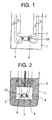
- Fig. 1 is a diagrammatic view of apparatus construction, illustrating an optic superconducting circuit element according to the present invention in which for its cooling means use is made of a refrigerator (cryocooler), and
- Fig. 2 is a diagrammatic view of apparatus construction, illustrating an optic superconducting circuit element according to the present invention in which for its cooling means use is made of liquid helium as a refrigerant (freezing medium).
- the optic superconducting circuit element of this invention is shown disposed in good thermal contact with a cold head 2 of the refrigerator that is in turn disposed within a chamber 1 to serve as the cooling means for cooling a superconductor to a temperature below its transition temperature Tc, the chamber 1 being evacuatable to a vacuum.
- the optic superconducting circuit element 10 includes a chip 3 and either a superconducting electromagnetic wave oscillating (generating and transmitting) source 5 constituted of a thin film superconductor fabricated on the chip 3 or a superconducting electromagnetic wave oscillating (generating and transmitting) source 5 constituted of a thin film single crystal film superconductor fabricated on the chip 3. Included also in the optic superconducting circuit element 10 is a superconducting Josephson junction device 4 constituted of a high temperature oxide superconductor disposed in close vicinity to the superconducting electromagnetic wave oscillating (generating and transmitting) source 5 on the chip 3 for detecting an electromagnetic wave from the superconducting electromagnetic wave oscillating (generating and transmitting) source 5.
- the superconducting electromagnetic wave oscillating (generating and transmitting) source 5 and the superconducting Josephson junction device 4 are designed to be supplied with electric currents separately from each other from their respective constant current bias sources (not shown).
- the optic superconducting circuit element 10 is disposed within a sample chamber 8 of a cooling apparatus 7 filled with liquid helium 6 as a cooling means for cooling the superconductor to a temperature below its transition temperature Tc and is mounted on a copper block 9 held in good thermal contact with the liquid helium.
- Fig. 3 is a diagrammatic view of appearance of an optic superconducting circuit element according to the present invention in which a superconducting electromagnetic wave oscillating (generating and transmitting) source 16 and a superconducting Josephson junction devices 14 are fabricated on a chip 3 by using a thin film of a superconductor formed thereon and a high temperature oxide superconductor formed also thereon.
- a superconducting electromagnetic wave oscillating (generating and transmitting) source 16 and a superconducting Josephson junction devices 14 are fabricated on a chip 3 by using a thin film of a superconductor formed thereon and a high temperature oxide superconductor formed also thereon.
- FIG. 4 is a diagrammatic view of appearance of an optic superconducting circuit element according to the present invention in which a superconducting electromagnetic wave oscillating (generating and transmitting) source 20 and a superconducting Josephson junction devices 14 are fabricated on a chip 3 by using a thin film, single crystal film of a superconductor formed thereon and a high temperature oxide superconductor formed also thereon. It should be noted here that the chip 3 is shown as taken out for one unit of the optic superconducting circuit element fabricated on a crystalline substrate.
- the optic superconducting circuit element 10 comprising the chip 3 for which use is made of a bi-crystalline substrate prepared by joining together a pair of single crystalline substrates crystallographically oriented at mutually different angles, either the superconducting electromagnetic wave oscillating (generating and transmitting) source 16 for which use is made of a thin film of superconductor formed on the chip 3 or the superconducting electromagnetic wave oscillating (generating and transmitting) source 20 for which use is made of a thin single crystal film of superconductor formed on the chip 3, and the superconducting Josephson junction device 14 for detecting electromagnetic waves, the device 14 having a constriction or necking 12 in its central area and formed with a Josephson junction 15 and for which use is made of a high temperature oxide superconductor.
- the superconducting Josephson junction device 14 is prepared by causing a thin film of high temperature oxide superconductor to grow on the bi-crystalline substrate from the substrates joined together and is then formed thereon naturally. If use is made of an ordinary single crystal substrate in lieu of the bi-crystalline substrate, then a Josephson junction to be formed is of layered thin-film type.
- the distance between the superconducting electromagnetic wave oscillating (generating and transmitting) source 16 and the superconducting Josephson junction device 14 although depending on the frequency bands of electromagnetic waves should desirably be generally within 1 mm or so, considering high sensitivity reception of a weak signal and so forth. This equally applies to the superconducting electromagnetic wave oscillating (generating and transmitting) source 20 using a thin film of single crystal superconductor.
- the superconducting electromagnetic wave oscillating (generating and transmitting) source 16 is formed, for example, by joining an Au metal electrode and an YBa 2 Cu 3 O 7-y high temperature oxide superconductor with a dielectric barrier layer to form a tunnel junction.
- the superconducting Josephson junction device 14 for use in detecting an electromagnetic wave is made of a superconductor that is preferably large in superconducting energy gap. Use should be made of, for example, an YBa 2 Cu 3 O 7-y high temperature oxide superconductor. While a low temperature superconductor has an energy gap as small as several meV, a high temperature oxide superconductor has an energy gap as large as several tens meV, one order greater than that.
- the superconductor material here is preferably La 2-x Sr x CuO 4 , Bi 2 Sr 2 CaCu 2 O y whose transition temperature is 80 K (hereafter referred to as "BSCCO”), Bi 2 Sr 2 Ca 2 Cu 3 O y whose transition temperature is 110 K, or YBa 2 Cu 3 O 7-y whose transition temperature is 80 to 90 K (hereafter referred to as "YBCO”), although any other high temperature oxide superconductor can be utilized insofar as it is satisfactory in crystallinity.
- BSCCO Bi 2 Sr 2 CaCu 2 O y whose transition temperature is 80 K
- YBCO YBa 2 Cu 3 O 7-y whose transition temperature is 80 to 90 K
- YBCOs include a superconductor in which a transition element is replaced for Y, such as, for example, ErBa 2 Cu 3 O 7-y and NdBa 2 Cu 3 O 7-y .
- a transition element such as, for example, ErBa 2 Cu 3 O 7-y and NdBa 2 Cu 3 O 7-y .
- high temperature superconductors are concerned whose transition temperatures are higher than the temperature of liquid nitrogen, it is possible to use liquid nitrogen in place of liquid helium.
- the suffixes x and y include 0 (zero).
- the superconducting electromagnetic wave oscillating (generating and transmitting) source 16 using a thin film of superconductor is supplied via J3 and J4 with electric currents from their respective constant current sources (not shown) to oscillate (generate and transmit) an electromagnetic wave.
- the electromagnetic wave is made incident onto the superconducting Josephson junction device 14 made of a high temperature oxide superconductor supplied via J1 and J2 with electric currents from their respective constant current sources.
- the electromagnetic wave made incident onto the Josephson junction 15 biased at a constant voltage is coupled to a high frequency electric current brought about by ac Josephson effect to cause it to appear as a change in its DC current component. If the input power signal is sufficiently small, its change has a zero-order change thereof primarily contributing thereto.
- Such a change in the DC component can be detected as a change in voltage according to the presence of irradiation of the Josephson junction 15 with an electromagnetic wave, thereby permitting the optic superconducting circuit element 10 to operate by oscillating (generating and transmitting) and receiving the electromagnetic wave.
- the superconducting electromagnetic wave source 20 using a thin single crystal film of superconductor is supplied via J3 and J4 with electric currents from their respective constant current sources (not shown) to oscillate (generate and transmit) an electromagnetic wave.
- the electromagnetic wave is made incident onto the superconducting Josephson junction device 14 made of a high temperature oxide superconductor supplied via J1 and J2 with electric currents from their respective constant current sources.
- the optic superconducting circuit element 10 oscillates (generates and transmits) and receives the electromagnetic wave.
- an optic superconducting circuit element having a superconducting electromagnetic wave oscillating (generating and transmitting) source 16 or 20 and a superconducting Josephson device 14 disposed and spaced from each other by a distance of about 1 mm or less on a single chip and in which for each of the superconducting electromagnetic wave oscillating (generating and transmitting) source 16, 20 and a superconducting Josephson device 14 use is made of a high temperature oxide superconductor that is large in superconducting energy gap, makes it possible to operate to oscillate (generate and transmit) electromagnetic waves over extended frequency bands ranging from microwave to THz bands and yet with a high sensitivity.
- Fig. 5 is a graph showing the current v. voltage characteristic of a superconducting Josephson junction device 14 using an YBa 2 Cu 3 O 7-y superconductor for the thin film of high temperature superconductor 14, including a graph showing a current by a voltage differential characteristic thereof.
- FIG. 6 shows results of measurement in an example in which a superconducting electromagnetic wave oscillating (generating and transmitting) source 16 using an YBa 2 Cu 3 O 7-y superconductor for the thin film of high temperature superconductor and made of Au/I/YBa 2 Cu 3 O 7-y (where I represents an dielectric barrier layer) is biased with electric currents of various current magnitudes (I inj ) to oscillate (generate and transmit) an electromagnetic wave in a THz frequency band, which is measured by a superconducting Josephson junction device shown in Fig. 5, located spaced apart therefrom at a distance of 0.7 mm.
- the superconducting electromagnetic wave oscillating (generating and transmitting) source 16 is biased with a fixed current magnitude (I inj ) to oscillate (generate and transmit) an electromagnetic wave and the voltage (V) applied across the Josephson junction 15 of the superconducting Josephson junction device 14 are varied successively between 0 and 6 mV.
- the ordinate represents changes in voltage ⁇ V as mentioned above and the abscissa represents the voltage V applied across the Josephson junction 15 as above.
- the frequency f is plotted along the abscissa represented at the top of each of the graphs in Fig. 6. While in the embodiments illustrated by the graphs shown in Fig.
- the present invention provides an optic superconducting circuit element that incorporates on a single chip superconducting electromagnetic wave oscillating (generating and transmitting) and receiving Josephson junctions, thereby making it possible to accomplish operations for both oscillating (generating and transmitting) and receiving electromagnetic waves in an extended frequency band, ranging from microwave to THz frequency bands and with high sensitivity.
- it should be highly useful in the field of superconducting micro-optoelectronics.
Landscapes
- Chemical & Material Sciences (AREA)
- Engineering & Computer Science (AREA)
- Ceramic Engineering (AREA)
- Superconductor Devices And Manufacturing Methods Thereof (AREA)
Abstract
Description
Claims (8)
- An optic superconducting circuit element, characterized in that it comprises a superconducting electromagnetic wave oscillating (generating and transmitting) source for oscillating (generating and transmitting) an electromagnetic wave and a superconducting Josephson junction device for receiving the electromagnetic wave transmitted from said superconducting electromagnetic wave oscillating (generating and transmitting) source, wherein said superconducting electromagnetic wave oscillating (generating and transmitting) source and said superconducting Josephson junction device are mounted on an identical and common chip.
- An optic superconducting circuit element as set forth in claim 1, characterized in that said superconducting electromagnetic wave oscillating (generating and transmitting) source and said superconducting Josephson junction device are so mounted as spaced from each other at a distance not greater than 1 mm.
- An optic superconducting circuit element as set forth in claim 1 or claim 2, characterized in that said superconducting Josephson junction device has a (Josephson) junction adapted to receive said electromagnetic wave transmitted from said superconducting electromagnetic wave oscillating (generating and transmitting) source and that the circuit element further comprises a means for detecting said electromagnetic wave in response to ac Josephson (alternating current) effect brought about at said junction by said electromagnetic wave incident thereon.
- An optic superconducting circuit element as set forth in any one of claim 1 to claim 3, characterized in that it further comprises a means for biasing said superconducting Josephson junction device with a fixed electric current and shifting the point of such biasing successively in response to a change occurring according to the presence or absence of the electromagnetic wave, thereby providing continuous spectral information thereof.
- An optic superconducting circuit element as set forth in any one of claim 1 to claim 4, characterized in that said electromagnetic wave has frequencies in a frequency band ranging from microwave to THz frequency bands.
- An optic superconducting circuit element as set forth in any one of claim 1 to claim 5, characterized in that each of said superconducting electromagnetic wave oscillating (generating and transmitting) source and said superconducting Josephson junction device is made of a superconductor that is large in superconducting energy gap to extend a detectable frequency band of the electromagnetic wave to cover a THz frequency band.
- An optic superconducting circuit element as set forth in any one of claim 1 to claim 6, characterized in that said superconductor is a high temperature oxide superconductor.
- An optic superconducting circuit element as set forth in any one of claim 1 to claim 7, characterized in that each of said superconducting electromagnetic wave oscillating (generating and transmitting) source and said superconducting Josephson junction device is made of a thin film, or a thin film, single crystal film.
Applications Claiming Priority (3)
| Application Number | Priority Date | Filing Date | Title |
|---|---|---|---|
| JP23008799 | 1999-08-16 | ||
| JP23008799 | 1999-08-16 | ||
| PCT/JP2000/005328 WO2001013439A1 (en) | 1999-08-16 | 2000-08-09 | Optical superconducting device |
Publications (3)
| Publication Number | Publication Date |
|---|---|
| EP1213774A1 true EP1213774A1 (en) | 2002-06-12 |
| EP1213774A4 EP1213774A4 (en) | 2007-07-18 |
| EP1213774B1 EP1213774B1 (en) | 2010-12-15 |
Family
ID=16902354
Family Applications (1)
| Application Number | Title | Priority Date | Filing Date |
|---|---|---|---|
| EP00951910A Expired - Lifetime EP1213774B1 (en) | 1999-08-16 | 2000-08-09 | Optical superconducting device |
Country Status (7)
| Country | Link |
|---|---|
| US (1) | US6815708B1 (en) |
| EP (1) | EP1213774B1 (en) |
| JP (1) | JP3864391B2 (en) |
| KR (1) | KR100546017B1 (en) |
| DE (1) | DE60045383D1 (en) |
| TW (1) | TW488093B (en) |
| WO (1) | WO2001013439A1 (en) |
Families Citing this family (15)
| Publication number | Priority date | Publication date | Assignee | Title |
|---|---|---|---|---|
| CN100444419C (en) * | 2006-04-14 | 2008-12-17 | 中国科学院上海技术物理研究所 | Terahertz photodetector with tunable detection wavelength |
| KR100899805B1 (en) * | 2006-07-04 | 2009-05-28 | 학교법인 포항공과대학교 | Terahertz electromagnetic wave emission and detecting device using Josephson vortex flow |
| US8571614B1 (en) | 2009-10-12 | 2013-10-29 | Hypres, Inc. | Low-power biasing networks for superconducting integrated circuits |
| CN102593235B (en) * | 2012-03-19 | 2014-09-03 | 中国科学院苏州纳米技术与纳米仿生研究所 | Microwave terahertz wave detector and preparation method thereof |
| US9296609B2 (en) | 2013-09-03 | 2016-03-29 | Northrop Grumman Systems Corporation | Optical-microwave-quantum transducer |
| US9260289B2 (en) * | 2013-09-03 | 2016-02-16 | Northrop Grumman Systems Corporation | Optical-microwave-quantum transducer |
| RU2581405C1 (en) * | 2015-02-05 | 2016-04-20 | Федеральное государственное бюджетное учреждение "Национальный исследовательский центр "Курчатовский институт" | Method of producing superconducting multiple-section optical detectors |
| US10222416B1 (en) | 2015-04-14 | 2019-03-05 | Hypres, Inc. | System and method for array diagnostics in superconducting integrated circuit |
| US9885888B2 (en) | 2016-02-08 | 2018-02-06 | International Business Machines Corporation | Integrated microwave-to-optical single-photon transducer with strain-induced electro-optic material |
| CN109029743B (en) * | 2018-08-08 | 2020-01-03 | 南开大学 | Microwave single photon detector, detection method and preparation method thereof |
| CN108761156B (en) * | 2018-08-24 | 2024-08-20 | 北京无线电计量测试研究所 | Solid-state refrigeration quantum voltage standard device |
| US11545288B2 (en) | 2020-04-15 | 2023-01-03 | Northrop Grumman Systems Corporation | Superconducting current control system |
| US11757467B2 (en) | 2021-08-13 | 2023-09-12 | Northrop Grumman Systems Corporation | Circuits for converting SFQ-based RZ and NRZ signaling to bilevel voltage NRZ signaling |
| US12597925B2 (en) | 2022-12-08 | 2026-04-07 | Northrop Grumman Systems Corporation | Superconducting current control system |
| US12395140B2 (en) | 2023-07-27 | 2025-08-19 | Northrop Grumman Systems Corporation | Non-return to zero (NRZ) amplifier system |
Family Cites Families (8)
| Publication number | Priority date | Publication date | Assignee | Title |
|---|---|---|---|---|
| JPH01302782A (en) | 1988-05-30 | 1989-12-06 | Mitsubishi Electric Corp | Photo detector |
| US5039951A (en) * | 1990-10-30 | 1991-08-13 | Bell Communications Research, Inc. | Josephson junction FSK demodulator |
| JPH05121910A (en) | 1991-07-30 | 1993-05-18 | Fujitsu Ltd | Circuit wiring device using the Josephson effect |
| JP3329127B2 (en) * | 1995-03-24 | 2002-09-30 | 松下電器産業株式会社 | Superconducting oscillator |
| US5570045A (en) | 1995-06-07 | 1996-10-29 | Lsi Logic Corporation | Hierarchical clock distribution system and method |
| JPH0964643A (en) * | 1995-08-23 | 1997-03-07 | Nippon Telegr & Teleph Corp <Ntt> | Superconducting oscillator and manufacturing method thereof |
| EP0823734A1 (en) * | 1996-07-23 | 1998-02-11 | DORNIER GmbH | Josephson junction array device, and manufacture thereof |
| JP4132193B2 (en) | 1998-03-23 | 2008-08-13 | 独立行政法人科学技術振興機構 | Superconducting terahertz electromagnetic wave generation module |
-
2000
- 2000-08-09 US US10/048,481 patent/US6815708B1/en not_active Expired - Fee Related
- 2000-08-09 DE DE60045383T patent/DE60045383D1/en not_active Expired - Lifetime
- 2000-08-09 WO PCT/JP2000/005328 patent/WO2001013439A1/en not_active Ceased
- 2000-08-09 EP EP00951910A patent/EP1213774B1/en not_active Expired - Lifetime
- 2000-08-09 KR KR1020017016429A patent/KR100546017B1/en not_active Expired - Fee Related
- 2000-08-09 JP JP2001517437A patent/JP3864391B2/en not_active Expired - Fee Related
- 2000-08-16 TW TW089116509A patent/TW488093B/en not_active IP Right Cessation
Also Published As
| Publication number | Publication date |
|---|---|
| EP1213774B1 (en) | 2010-12-15 |
| KR100546017B1 (en) | 2006-01-25 |
| WO2001013439A1 (en) | 2001-02-22 |
| JP3864391B2 (en) | 2006-12-27 |
| TW488093B (en) | 2002-05-21 |
| EP1213774A4 (en) | 2007-07-18 |
| US6815708B1 (en) | 2004-11-09 |
| DE60045383D1 (en) | 2011-01-27 |
| KR20020010724A (en) | 2002-02-04 |
Similar Documents
| Publication | Publication Date | Title |
|---|---|---|
| US6815708B1 (en) | Optical superconducting device | |
| Langenberg et al. | Josephson-type superconducting tunnel junctions as generators of microwave and submillimeter wave radiation | |
| Anlage et al. | A current controlled variable delay superconducting transmission line | |
| Gaidis et al. | Characterization of low-noise quasi-optical SIS mixers for the submillimeter band | |
| EP0734080A1 (en) | Superconducting junction device | |
| JPWO2001013439A1 (en) | Optical superconducting circuit elements | |
| Richards et al. | Millimeter and submillimeter wave detection and mixing with superconducting weak links | |
| McGrath et al. | Accurate experimental and theoretical comparisons between superconductor‐insulator‐superconductor mixers showing weak and strong quantum effects | |
| Il’in et al. | Microwave mixing in microbridges made from YBa 2 Cu 3 O 7− x thin films | |
| Konopka et al. | Microwave detectors based on granular high-T/sub c/thin films | |
| Liu et al. | Terahertz high-sensitivity SIS mixer based on Nb–AlN–NbN hybrid superconducting tunnel junctions | |
| Kinev et al. | Superconducting Integrated Microcircuits Based on NbTiN/Al Transmission Lines Operating at Frequencies Above 1 THz | |
| Shi et al. | Low-noise superconducting receivers for millimeter and submillimeter wavelengths | |
| Harnack et al. | HTS mixers based on the Josephson effect and on the hot-electron bolometric effect | |
| Khan et al. | Superconducting terahertz generators | |
| Carpenter et al. | 100 GHz SIS mixer with improved rf matching | |
| Constantinian et al. | Shot noise in YBCO bicrystal Josephson junctions | |
| Kulikov et al. | A MM-wave radiometer with planar Nb/a-Si/Nb Josephson junction | |
| Belitsky et al. | Low-Noise Superconducting Mixers for the Terahertz Frequency Range | |
| Yoshisato et al. | Mixing characteristics of a microwave detector using a granular YBCO superconductor | |
| Yu et al. | Terahertz Antenna Characterization by the Josephson Effect for Superconducting Terahertz Detectors | |
| Jensen et al. | Resonator coupled Josephson junctions; parametric excitations and mutual locking | |
| Ermakov et al. | SNAP structures with Nb-AlO/sub x/-Nb junctions for MM-wave receivers | |
| Khan et al. | Spectrum of oscillation of the array of Josephson junctions in the coplanar line | |
| Chen et al. | Limiting performance of YBCO high-frequency Josephson devices |
Legal Events
| Date | Code | Title | Description |
|---|---|---|---|
| PUAI | Public reference made under article 153(3) epc to a published international application that has entered the european phase |
Free format text: ORIGINAL CODE: 0009012 |
|
| 17P | Request for examination filed |
Effective date: 20020305 |
|
| AK | Designated contracting states |
Kind code of ref document: A1 Designated state(s): AT BE CH CY DE DK ES FI FR GB GR IE IT LI LU MC NL PT SE |
|
| RAP1 | Party data changed (applicant data changed or rights of an application transferred) |
Owner name: JAPAN SCIENCE AND TECHNOLOGY AGENCY |
|
| RBV | Designated contracting states (corrected) |
Designated state(s): AT BE CH DE FR GB LI |
|
| A4 | Supplementary search report drawn up and despatched |
Effective date: 20070620 |
|
| 17Q | First examination report despatched |
Effective date: 20071011 |
|
| RIC1 | Information provided on ipc code assigned before grant |
Ipc: H01L 27/18 20060101ALI20100512BHEP Ipc: H01L 39/22 20060101AFI20100512BHEP |
|
| GRAP | Despatch of communication of intention to grant a patent |
Free format text: ORIGINAL CODE: EPIDOSNIGR1 |
|
| RBV | Designated contracting states (corrected) |
Designated state(s): DE FR GB |
|
| RAP1 | Party data changed (applicant data changed or rights of an application transferred) |
Owner name: JAPAN SCIENCE AND TECHNOLOGY AGENCY |
|
| GRAS | Grant fee paid |
Free format text: ORIGINAL CODE: EPIDOSNIGR3 |
|
| GRAA | (expected) grant |
Free format text: ORIGINAL CODE: 0009210 |
|
| AK | Designated contracting states |
Kind code of ref document: B1 Designated state(s): DE FR GB |
|
| REG | Reference to a national code |
Ref country code: GB Ref legal event code: FG4D |
|
| REF | Corresponds to: |
Ref document number: 60045383 Country of ref document: DE Date of ref document: 20110127 Kind code of ref document: P |
|
| PLBE | No opposition filed within time limit |
Free format text: ORIGINAL CODE: 0009261 |
|
| STAA | Information on the status of an ep patent application or granted ep patent |
Free format text: STATUS: NO OPPOSITION FILED WITHIN TIME LIMIT |
|
| 26N | No opposition filed |
Effective date: 20110916 |
|
| PGFP | Annual fee paid to national office [announced via postgrant information from national office to epo] |
Ref country code: GB Payment date: 20110819 Year of fee payment: 12 Ref country code: FR Payment date: 20110901 Year of fee payment: 12 Ref country code: DE Payment date: 20110823 Year of fee payment: 12 |
|
| REG | Reference to a national code |
Ref country code: DE Ref legal event code: R097 Ref document number: 60045383 Country of ref document: DE Effective date: 20110916 |
|
| GBPC | Gb: european patent ceased through non-payment of renewal fee |
Effective date: 20120809 |
|
| REG | Reference to a national code |
Ref country code: FR Ref legal event code: ST Effective date: 20130430 |
|
| PG25 | Lapsed in a contracting state [announced via postgrant information from national office to epo] |
Ref country code: DE Free format text: LAPSE BECAUSE OF NON-PAYMENT OF DUE FEES Effective date: 20130301 Ref country code: GB Free format text: LAPSE BECAUSE OF NON-PAYMENT OF DUE FEES Effective date: 20120809 |
|
| PG25 | Lapsed in a contracting state [announced via postgrant information from national office to epo] |
Ref country code: FR Free format text: LAPSE BECAUSE OF NON-PAYMENT OF DUE FEES Effective date: 20120831 |
|
| REG | Reference to a national code |
Ref country code: DE Ref legal event code: R119 Ref document number: 60045383 Country of ref document: DE Effective date: 20130301 |