EP1213772B1 - Photovoltaic apparatus with spherical semiconductor particles - Google Patents
Photovoltaic apparatus with spherical semiconductor particles Download PDFInfo
- Publication number
- EP1213772B1 EP1213772B1 EP01204475A EP01204475A EP1213772B1 EP 1213772 B1 EP1213772 B1 EP 1213772B1 EP 01204475 A EP01204475 A EP 01204475A EP 01204475 A EP01204475 A EP 01204475A EP 1213772 B1 EP1213772 B1 EP 1213772B1
- Authority
- EP
- European Patent Office
- Prior art keywords
- photoelectric conversion
- semiconductor layer
- conductor
- conversion elements
- photovoltaic apparatus
- Prior art date
- Legal status (The legal status is an assumption and is not a legal conclusion. Google has not performed a legal analysis and makes no representation as to the accuracy of the status listed.)
- Expired - Lifetime
Links
Images



Classifications
-
- H—ELECTRICITY
- H10—SEMICONDUCTOR DEVICES; ELECTRIC SOLID-STATE DEVICES NOT OTHERWISE PROVIDED FOR
- H10F—INORGANIC SEMICONDUCTOR DEVICES SENSITIVE TO INFRARED RADIATION, LIGHT, ELECTROMAGNETIC RADIATION OF SHORTER WAVELENGTH OR CORPUSCULAR RADIATION
- H10F19/00—Integrated devices, or assemblies of multiple devices, comprising at least one photovoltaic cell covered by group H10F10/00, e.g. photovoltaic modules
-
- C—CHEMISTRY; METALLURGY
- C30—CRYSTAL GROWTH
- C30B—SINGLE-CRYSTAL GROWTH; UNIDIRECTIONAL SOLIDIFICATION OF EUTECTIC MATERIAL OR UNIDIRECTIONAL DEMIXING OF EUTECTOID MATERIAL; REFINING BY ZONE-MELTING OF MATERIAL; PRODUCTION OF A HOMOGENEOUS POLYCRYSTALLINE MATERIAL WITH DEFINED STRUCTURE; SINGLE CRYSTALS OR HOMOGENEOUS POLYCRYSTALLINE MATERIAL WITH DEFINED STRUCTURE; AFTER-TREATMENT OF SINGLE CRYSTALS OR A HOMOGENEOUS POLYCRYSTALLINE MATERIAL WITH DEFINED STRUCTURE; APPARATUS THEREFOR
- C30B11/00—Single-crystal growth by normal freezing or freezing under temperature gradient, e.g. Bridgman-Stockbarger method
- C30B11/003—Heating or cooling of the melt or the crystallised material
-
- C—CHEMISTRY; METALLURGY
- C30—CRYSTAL GROWTH
- C30B—SINGLE-CRYSTAL GROWTH; UNIDIRECTIONAL SOLIDIFICATION OF EUTECTIC MATERIAL OR UNIDIRECTIONAL DEMIXING OF EUTECTOID MATERIAL; REFINING BY ZONE-MELTING OF MATERIAL; PRODUCTION OF A HOMOGENEOUS POLYCRYSTALLINE MATERIAL WITH DEFINED STRUCTURE; SINGLE CRYSTALS OR HOMOGENEOUS POLYCRYSTALLINE MATERIAL WITH DEFINED STRUCTURE; AFTER-TREATMENT OF SINGLE CRYSTALS OR A HOMOGENEOUS POLYCRYSTALLINE MATERIAL WITH DEFINED STRUCTURE; APPARATUS THEREFOR
- C30B11/00—Single-crystal growth by normal freezing or freezing under temperature gradient, e.g. Bridgman-Stockbarger method
- C30B11/006—Controlling or regulating
-
- C—CHEMISTRY; METALLURGY
- C30—CRYSTAL GROWTH
- C30B—SINGLE-CRYSTAL GROWTH; UNIDIRECTIONAL SOLIDIFICATION OF EUTECTIC MATERIAL OR UNIDIRECTIONAL DEMIXING OF EUTECTOID MATERIAL; REFINING BY ZONE-MELTING OF MATERIAL; PRODUCTION OF A HOMOGENEOUS POLYCRYSTALLINE MATERIAL WITH DEFINED STRUCTURE; SINGLE CRYSTALS OR HOMOGENEOUS POLYCRYSTALLINE MATERIAL WITH DEFINED STRUCTURE; AFTER-TREATMENT OF SINGLE CRYSTALS OR A HOMOGENEOUS POLYCRYSTALLINE MATERIAL WITH DEFINED STRUCTURE; APPARATUS THEREFOR
- C30B29/00—Single crystals or homogeneous polycrystalline material with defined structure characterised by the material or by their shape
- C30B29/02—Elements
- C30B29/06—Silicon
-
- C—CHEMISTRY; METALLURGY
- C30—CRYSTAL GROWTH
- C30B—SINGLE-CRYSTAL GROWTH; UNIDIRECTIONAL SOLIDIFICATION OF EUTECTIC MATERIAL OR UNIDIRECTIONAL DEMIXING OF EUTECTOID MATERIAL; REFINING BY ZONE-MELTING OF MATERIAL; PRODUCTION OF A HOMOGENEOUS POLYCRYSTALLINE MATERIAL WITH DEFINED STRUCTURE; SINGLE CRYSTALS OR HOMOGENEOUS POLYCRYSTALLINE MATERIAL WITH DEFINED STRUCTURE; AFTER-TREATMENT OF SINGLE CRYSTALS OR A HOMOGENEOUS POLYCRYSTALLINE MATERIAL WITH DEFINED STRUCTURE; APPARATUS THEREFOR
- C30B29/00—Single crystals or homogeneous polycrystalline material with defined structure characterised by the material or by their shape
- C30B29/60—Single crystals or homogeneous polycrystalline material with defined structure characterised by the material or by their shape characterised by shape
- C30B29/66—Crystals of complex geometrical shape, e.g. tubes, cylinders
-
- C—CHEMISTRY; METALLURGY
- C30—CRYSTAL GROWTH
- C30B—SINGLE-CRYSTAL GROWTH; UNIDIRECTIONAL SOLIDIFICATION OF EUTECTIC MATERIAL OR UNIDIRECTIONAL DEMIXING OF EUTECTOID MATERIAL; REFINING BY ZONE-MELTING OF MATERIAL; PRODUCTION OF A HOMOGENEOUS POLYCRYSTALLINE MATERIAL WITH DEFINED STRUCTURE; SINGLE CRYSTALS OR HOMOGENEOUS POLYCRYSTALLINE MATERIAL WITH DEFINED STRUCTURE; AFTER-TREATMENT OF SINGLE CRYSTALS OR A HOMOGENEOUS POLYCRYSTALLINE MATERIAL WITH DEFINED STRUCTURE; APPARATUS THEREFOR
- C30B30/00—Production of single crystals or homogeneous polycrystalline material with defined structure characterised by the action of electric or magnetic fields, wave energy or other specific physical conditions
- C30B30/06—Production of single crystals or homogeneous polycrystalline material with defined structure characterised by the action of electric or magnetic fields, wave energy or other specific physical conditions using mechanical vibrations
-
- H—ELECTRICITY
- H02—GENERATION; CONVERSION OR DISTRIBUTION OF ELECTRIC POWER
- H02S—GENERATION OF ELECTRIC POWER BY CONVERSION OF INFRARED RADIATION, VISIBLE LIGHT OR ULTRAVIOLET LIGHT, e.g. USING PHOTOVOLTAIC [PV] MODULES
- H02S40/00—Components or accessories in combination with PV modules, not provided for in groups H02S10/00 - H02S30/00
- H02S40/30—Electrical components
- H02S40/36—Electrical components characterised by special electrical interconnection means between two or more PV modules, e.g. electrical module-to-module connection
-
- H—ELECTRICITY
- H10—SEMICONDUCTOR DEVICES; ELECTRIC SOLID-STATE DEVICES NOT OTHERWISE PROVIDED FOR
- H10F—INORGANIC SEMICONDUCTOR DEVICES SENSITIVE TO INFRARED RADIATION, LIGHT, ELECTROMAGNETIC RADIATION OF SHORTER WAVELENGTH OR CORPUSCULAR RADIATION
- H10F10/00—Individual photovoltaic cells, e.g. solar cells
- H10F10/10—Individual photovoltaic cells, e.g. solar cells having potential barriers
- H10F10/16—Photovoltaic cells having only PN heterojunction potential barriers
- H10F10/164—Photovoltaic cells having only PN heterojunction potential barriers comprising heterojunctions with Group IV materials, e.g. ITO/Si or GaAs/SiGe photovoltaic cells
- H10F10/165—Photovoltaic cells having only PN heterojunction potential barriers comprising heterojunctions with Group IV materials, e.g. ITO/Si or GaAs/SiGe photovoltaic cells the heterojunctions being Group IV-IV heterojunctions, e.g. Si/Ge, SiGe/Si or Si/SiC photovoltaic cells
-
- H—ELECTRICITY
- H10—SEMICONDUCTOR DEVICES; ELECTRIC SOLID-STATE DEVICES NOT OTHERWISE PROVIDED FOR
- H10F—INORGANIC SEMICONDUCTOR DEVICES SENSITIVE TO INFRARED RADIATION, LIGHT, ELECTROMAGNETIC RADIATION OF SHORTER WAVELENGTH OR CORPUSCULAR RADIATION
- H10F19/00—Integrated devices, or assemblies of multiple devices, comprising at least one photovoltaic cell covered by group H10F10/00, e.g. photovoltaic modules
- H10F19/90—Structures for connecting between photovoltaic cells, e.g. interconnections or insulating spacers
- H10F19/902—Structures for connecting between photovoltaic cells, e.g. interconnections or insulating spacers for series or parallel connection of photovoltaic cells
- H10F19/906—Structures for connecting between photovoltaic cells, e.g. interconnections or insulating spacers for series or parallel connection of photovoltaic cells characterised by the materials of the structures
-
- H—ELECTRICITY
- H10—SEMICONDUCTOR DEVICES; ELECTRIC SOLID-STATE DEVICES NOT OTHERWISE PROVIDED FOR
- H10F—INORGANIC SEMICONDUCTOR DEVICES SENSITIVE TO INFRARED RADIATION, LIGHT, ELECTROMAGNETIC RADIATION OF SHORTER WAVELENGTH OR CORPUSCULAR RADIATION
- H10F71/00—Manufacture or treatment of devices covered by this subclass
- H10F71/121—The active layers comprising only Group IV materials
-
- H—ELECTRICITY
- H10—SEMICONDUCTOR DEVICES; ELECTRIC SOLID-STATE DEVICES NOT OTHERWISE PROVIDED FOR
- H10F—INORGANIC SEMICONDUCTOR DEVICES SENSITIVE TO INFRARED RADIATION, LIGHT, ELECTROMAGNETIC RADIATION OF SHORTER WAVELENGTH OR CORPUSCULAR RADIATION
- H10F77/00—Constructional details of devices covered by this subclass
- H10F77/10—Semiconductor bodies
- H10F77/14—Shape of semiconductor bodies; Shapes, relative sizes or dispositions of semiconductor regions within semiconductor bodies
- H10F77/147—Shapes of bodies
-
- H—ELECTRICITY
- H10—SEMICONDUCTOR DEVICES; ELECTRIC SOLID-STATE DEVICES NOT OTHERWISE PROVIDED FOR
- H10F—INORGANIC SEMICONDUCTOR DEVICES SENSITIVE TO INFRARED RADIATION, LIGHT, ELECTROMAGNETIC RADIATION OF SHORTER WAVELENGTH OR CORPUSCULAR RADIATION
- H10F77/00—Constructional details of devices covered by this subclass
- H10F77/40—Optical elements or arrangements
- H10F77/42—Optical elements or arrangements directly associated or integrated with photovoltaic cells, e.g. light-reflecting means or light-concentrating means
- H10F77/488—Reflecting light-concentrating means, e.g. parabolic mirrors or concentrators using total internal reflection
-
- H—ELECTRICITY
- H10—SEMICONDUCTOR DEVICES; ELECTRIC SOLID-STATE DEVICES NOT OTHERWISE PROVIDED FOR
- H10F—INORGANIC SEMICONDUCTOR DEVICES SENSITIVE TO INFRARED RADIATION, LIGHT, ELECTROMAGNETIC RADIATION OF SHORTER WAVELENGTH OR CORPUSCULAR RADIATION
- H10F77/00—Constructional details of devices covered by this subclass
- H10F77/93—Interconnections
- H10F77/933—Interconnections for devices having potential barriers
- H10F77/935—Interconnections for devices having potential barriers for photovoltaic devices or modules
-
- Y—GENERAL TAGGING OF NEW TECHNOLOGICAL DEVELOPMENTS; GENERAL TAGGING OF CROSS-SECTIONAL TECHNOLOGIES SPANNING OVER SEVERAL SECTIONS OF THE IPC; TECHNICAL SUBJECTS COVERED BY FORMER USPC CROSS-REFERENCE ART COLLECTIONS [XRACs] AND DIGESTS
- Y02—TECHNOLOGIES OR APPLICATIONS FOR MITIGATION OR ADAPTATION AGAINST CLIMATE CHANGE
- Y02E—REDUCTION OF GREENHOUSE GAS [GHG] EMISSIONS, RELATED TO ENERGY GENERATION, TRANSMISSION OR DISTRIBUTION
- Y02E10/00—Energy generation through renewable energy sources
- Y02E10/50—Photovoltaic [PV] energy
- Y02E10/52—PV systems with concentrators
-
- Y—GENERAL TAGGING OF NEW TECHNOLOGICAL DEVELOPMENTS; GENERAL TAGGING OF CROSS-SECTIONAL TECHNOLOGIES SPANNING OVER SEVERAL SECTIONS OF THE IPC; TECHNICAL SUBJECTS COVERED BY FORMER USPC CROSS-REFERENCE ART COLLECTIONS [XRACs] AND DIGESTS
- Y02—TECHNOLOGIES OR APPLICATIONS FOR MITIGATION OR ADAPTATION AGAINST CLIMATE CHANGE
- Y02E—REDUCTION OF GREENHOUSE GAS [GHG] EMISSIONS, RELATED TO ENERGY GENERATION, TRANSMISSION OR DISTRIBUTION
- Y02E10/00—Energy generation through renewable energy sources
- Y02E10/50—Photovoltaic [PV] energy
- Y02E10/547—Monocrystalline silicon PV cells
-
- Y—GENERAL TAGGING OF NEW TECHNOLOGICAL DEVELOPMENTS; GENERAL TAGGING OF CROSS-SECTIONAL TECHNOLOGIES SPANNING OVER SEVERAL SECTIONS OF THE IPC; TECHNICAL SUBJECTS COVERED BY FORMER USPC CROSS-REFERENCE ART COLLECTIONS [XRACs] AND DIGESTS
- Y02—TECHNOLOGIES OR APPLICATIONS FOR MITIGATION OR ADAPTATION AGAINST CLIMATE CHANGE
- Y02P—CLIMATE CHANGE MITIGATION TECHNOLOGIES IN THE PRODUCTION OR PROCESSING OF GOODS
- Y02P70/00—Climate change mitigation technologies in the production process for final industrial or consumer products
- Y02P70/50—Manufacturing or production processes characterised by the final manufactured product
Definitions
- the present invention relates to a photovoltaic apparatus and to a mass-producing apparatus for mass-producing spherical semiconductor particles, suitable for manufacture of photovoltaic apparatus and the like.
- pin junction is to be construed as including a structure that n-, I- and p-type semiconductor layers are formed on an approximately spherical photoelectric conversion element so as to be arranged in this order outward from the inside of the approximately spherical photoelectric conversion element or inward from the outside.
- a typical related art technique provides a photovoltaic apparatus comprising a photoelectric conversion element composed of a crystal silicon semiconductor wafer.
- the related art photovoltaic apparatus is of cost expenditure because the step for producing a crystal is complex.
- the step for manufacturing a semiconductor wafer is not only complex because it includes cutting of a bulk single crystal, slicing, and polishing, but also the step is wasteful because crystal waste produced by the cutting, slicing, polishing etc. amounts to about 50% by volume or more of the original bulk single crystal.
- a photovoltaic apparatus comprising a photoelectric conversion element composed of an amorphous silicon (abbreviated as "a-Si") thin film, which solves the above-mentioned problems. Since a thin-film photoelectric conversion layer is formed by the plasma CVD (chemical vapor deposition) method, this related art photovoltaic apparatus has advantages that the steps which are conventionally required, such as cutting of a bulk single crystal, slicing, and polishing, are not necessary and that a deposited film can be used in its entirety as device active layers.
- a-Si amorphous silicon
- the amorphous silicon photovoltaic apparatus has a drawback that the semiconductor has a number of crystal defects (i.e., gap states) inside the semiconductor due to the amorphous structure, the amorphous silicon solar battery has a problem that the photoelectric conversion efficiency decreases due to a photo-induced deterioration phenomenon.
- a technique of inactivating crystal defects by applying hydrogenation treatment has been developed, whereby the manufacture of such electronic devices as an amorphous silicon solar battery has been realized.
- the amorphous silicon solar battery still has a weak point that the photoelectric conversion efficiency decreases by 15% to 25%.
- a recently developed technique for suppressing the photo-induced deterioration has realized a stack-type solar battery in which a photoelectrically active i-type layer is made extremely thin and 2-junction or 3-junction solar cells are used, and has succeeded in suppressing the photo-induced deterioration to about 10%. It has become apparent that the degree of photo-induced deterioration decreases when the operation temperature of solar cells is high. Although a module technique in which solar cells are caused to operate in such a condition is now being developed, it does not satisfy all the requirements and further improvements are required.
- a solar array is formed in the following manner. Spherical particles each having a p-type silicon sphere and an n-type silicon skin are buried in a flat sheet of aluminum foil having holes. The internal p-type silicon spheres are exposed by etching away the n-type silicon skins from the back side of the aluminum foil. The exposed-type silicon spheres are connected to another sheet of aluminum foil.
- Such spherical semiconductor particles are required in order to manufacture a solar array such as one disclosed in JP-B2 7-54855 .
- photoelectromotive force generated by applying light to silicon spherical semiconductor particles can be obtained by electrically connecting the silicon spherical semiconductor particles to the metal foil matrix.
- such spherical particles are manufactured in such a manner that a solid-state material is crushed into particles having irregular outer shapes, resulting particles are put in a cylinder that is provided with a lining for grinding, and a gas eddy flow is formed in the cylinder to thereby collide the particles with the lining or with each other.
- This related art technique requires much time and labor to manufacture spherical semiconductor particles and hence is inferior in cost reduction aspect.
- a thin silicon rod is manufactured in the following manner. A tip portion of a silicon rod that is vertically held is melted by high-frequency heating. After a seed silicon crystal is fusion-bonded to the molten silicon rod, the seed silicon crystal and the silicon rod are moved away from each other in the vertical direction, whereby a thin silicon rod that is less than 1 mm in thickness is obtained. According to this prior art technique, a thin silicon rod is manufactured at a rate of 5 mm/min to 10 mm/min, for example. It is desired that a large number of spherical semiconductor particles be manufactured at much higher rate.
- An object of the present invention is to provide a highly reliable, highly efficient photovoltaic apparatus that can be mass-produced easily while the used amount of semiconductor material such as high-purity silicon is decreased, that is, a highly reliable, high-efficiency photovoltaic apparatus that can be manufactured at low costs with smaller amounts of consumption of resources and energy.
- Another object of the invention is to provide an apparatus capable of mass-producing spherical semiconductor particles easily by simple manipulations.
- a first aspect of the invention provides a photovoltaic apparatus according to claim 1.
- the approximately spherical photoelectric conversion elements are disposed in the respective recesses of the support and the inside surfaces of the respective recesses are constituted by the first conductor or the coating formed on the first conductor. Therefore, external light such as sunlight is directly applied to each of the photoelectric conversion elements as well as after being reflected by the part of the first conductor or coating formed on the first conductor which is the inside surface of the recess.
- the photoelectric conversion elements are disposed in the respective recesses, intervals are formed in between, that is, their arrangement is not dense. However, the number of photoelectric conversion elements used is decreased, with the result that the used amount of high-purity material (e.g., silicon) of the photoelectric conversion elements can be reduced and the step of connecting the photoelectric conversion elements to the conductors of the support can be made easier.
- high-purity material e.g., silicon
- the recesses are arranged adj acent to each other, whereby external light is reflected by the inside surfaces of the recesses and then applied to the photoelectric conversion elements. Therefore, external light can be efficiently used for generation of photoelectromotive force by the photoelectric conversion elements. Accordingly it is achieved to maximize the electric power generation amount per unit area opposed to a light source of the photoelectric conversion elements.
- the photoelectric conversion elements may be made of a single-crystal, polycrystalline, or amorphous material and may be made of a silicon material, a compound semiconductor material, or the like.
- the photoelectric conversion elements may have a pn structure, a pin structure, a Schottky barrier structure, a MIS (metal-insulator-semiconductor) structure, a homo junction structure, a heterojunction structure, or the like.
- the inside first semiconductor layer is partially exposed through the opening of the outside second semiconductor layer, which makes it possible to take out photoelectromotive force that is generated between the first and second semiconductor layers during application of light.
- the second semiconductor layers of the respective photoelectric conversion elements disposed in the respective recesses of the support are electrically connected to the first conductor of the support.
- the exposed portions of the inside first semiconductor layers of the respective photoelectric conversion elements are electrically connected to the second conductor which is formed on the first conductor with the insulator interposed in between.
- the photoelectric conversion elements are connected to each other in parallel with the first and second conductors and can produce a large current.
- the photoelectric conversion element may either be a complete sphere or have an outer surface that is approximately a complete spherical surface.
- the first semiconductor layer may be solid and have an approximately spherical shape.
- the first semiconductor layer may be formed on the outer surface of a core that is prepared in advance.
- the approximately spherical first semiconductor layer may have a hollow central portion.
- the photoelectric conversion elements have an outer diameter of 0.5 mm to 2.0 mm.
- the photoelectric conversion elements may have an outer diameter of 0.5 mm to 2.0 mm, preferably of 0.8 to 1.2 mm, more preferably of about 1. 0 mm. This makes it possible to sufficiently reduce the used amount of material such as high-purity silicon and to maximize the electric power generation amount. Further, the spherical photoelectric conversion elements can be handled easily during manufacture and the productivity can be increased.
- the opening of the second semiconductor layer has a central angle ⁇ 1 of 45° to 90°.
- the central angle ⁇ 1 By setting the central angle ⁇ 1 at 45° to 90°, preferably at 60° to 90°, the amounts of those parts of the first and second semiconductor layers which are discarded to form the opening can be reduced, that is, the loss of material can be reduced. Further, setting the central angle ⁇ 1 in such a range allows the opening to have a sufficient area for the electrical connection between the first semiconductor layer and the second conductor of the support.
- the recesses of the support have respective openings of a polygon (e.g., honeycomb polygon) of which ones adjacent to each other are continuous, that each of the recesses narrows toward a bottom thereof, and the first semiconductor layer and second semiconductor layer of each of the photoelectric conversion elements are electrically connected to the second conductor and the first conductor, respectively, at the bottom or in a vicinity thereof of the recess.
- a polygon e.g., honeycomb polygon
- the first conductor is provided with a circular first connection hole formed at the bottom or in a vicinity thereof of the recess and the insulator is provided with a circular second connection hole having a common axial line with the first connection hole, that a portion of the photoelectric conversion element in a vicinity of the opening of the second semiconductor layer fits in the first connection hole and an outer surface portion above the opening of the second semiconductor layer is electrically connected to an end face of the first connection hole of the first conductor or to a portion thereof in the vicinity of the end face, and that the exposed portion of the first semiconductor layer of the photoelectric conversion element is electrically connected to the second conductor through the second connection hole.
- an outer diameter D1 of the photoelectric conversion elements, an inner diameter D2 of the openings of the second semiconductor layers, and an inner diameter D3 of the first connection holes, and an inner diameter D4 of the second connection holes satisfy a relationship D1 > D3 > D2 > D4.
- a portion of the photoelectric conversion element in the vicinity of the opening fits in the first connection hole of the first conductor and the exposed portion of the first semiconductor layer of the photoelectric conversion element is electrically connected to the second conductor through the second connection hole of the insulator of the support, the first conductor and the second conductor of the support can easily be connected electrically to the second semiconductor layer and the first semiconductor layer, respectively, of the photoelectric conversion element.
- a portion, above the opening, of the outer surface of the second semiconductor layer is electrically connected to the end face of the first connection hole and/or a portion of the first conductor in the vicinity of the end face, that is, the inner circumferential face of the first connection hole and/or a portion of the first conductor in the vicinity of and surrounding the first connection hole (see Fig. 1 ).
- each projection of the second conductor formed by elastic deformation may be inserted through the second connection hole and electrically connected to the portion of the first semiconductor layer that is exposed through the opening.
- the portion of the first semiconductor layer that is exposed through the opening may be connected to the second conductor with conductive paste provided in the second connection hole or via a conductive bump such as a metal bump.
- a light-gathering ratio x which equals to S1/S2 is selected to be in a range of 2 to 8, wherein SI is an opening area of each of the recesses of the support and S2 is an area of a cross-section of the photoelectric conversion elements including a center thereof.
- a second aspect of the invention provides a photovoltaic apparatus according to claim 8.
- a third aspect of the invention provides a photovoltaic apparatus according to claim 9.
- the openings of the respective recesses of the support assume honeycomb polygons such as hexagon. Each recess narrows toward its bottom, and a photoelectric conversion element is disposed at the bottom of each recess. Each photoelectric conversion element is electrically connected to the conductors of the support at the bottom or its neighborhood of the recess. Since the openings of the respective recesses assume polygons and are continuous with each other, all the light received by all the surface of the support opposed to a light source (e.g., sunlight) excluding the areas of the photoelectric conversion elements can be applied to the photoelectric conversion elements.
- a light source e.g., sunlight
- S1/S2 the light-gathering ratio
- the silicon single crystal is as thick as 350 ⁇ m to 500 ⁇ m and the thickness amounts to about 1 mm when the slice loss is included. Therefore, in the first prior art technique, the amount of silicon that is used for generating an electric power of 1 W is about 15 to 20 g. It is understood that the invention can make the used amount of silicon much smaller than in the first prior art technique.
- the number of necessary photoelectric conversion elements can be decreased and the amount of silicon used for generating an electric power of 1 W could further be reduced.
- the light-gathering efficiency which is the ratio of optical energy absorbed by the photoelectric conversion elements to that incident on the recesses becomes smaller and the performance of the photovoltaic apparatus lowers accordingly.
- the outer diameter of each photoelectric conversion element at 0.5 mm to 2.0 mm (preferably 0.8 mm to 1.2 mm) and setting the light-gathering ratio x at 2 to 8 (preferably 4 to 6), the number of photoelectric conversion elements can be decreased, the amount of silicon used for generating an electric power of 1 W can be reduced, and the step of electrically connecting the photoelectric conversion elements to the support can further be simplified.
- the combination of the values of the outer diameter of each photoelectric conversion element and the light gathering ratio x is important in decreasing the number of photoelectric conversion elements and reducing the amount of silicon used for generating an electric power of 1 W.
- each photoelectric conversion element When the outer diameter of each photoelectric conversion element is smaller than 0.5 mm, the number of necessary photoelectric conversion elements becomes unduly large though the used amount of silicon decreases. When the outer diameter of each photoelectric conversion element is greater than 2 mm, the used amount of silicon becomes unduly large though the number of necessary photoelectric conversion elements decreases.
- the invention makes it possible to make the light-gathering efficiency greater than 80% or even 90%.
- the temperature of the photoelectric conversion elements can be increased to 40°C to 80°C, which is higher than in the case of using an amorphous silicon, thin-plate photoelectric conversion element. This makes it possible to suppress deterioration of the amorphous silicon photoelectric conversion element and to thereby elongate the life of the photovoltaic apparatus.
- the photoelectric conversion elements have a pn junction in such a manner that the second semiconductor layer of one conductivity type having a wider optical band gap than the first semiconductor layer having the other conductivity type does is formed outside the first semiconductor layer ⁇ see Fig. 14 ⁇ .
- the photoelectric conversion elements have a pin junction in such a manner that the first semiconductor layer having one conductivity type, an amorphous intrinsic semiconductor layer, and an amorphous second semiconductor layer of the other conductivity type having a wider optical band gap than the first semiconductor layer does are arranged outward in this order (see Figs. 15 and 16 ).
- the first semiconductor layer and the second semiconductor layer are made of n-type silicon and p-type amorphous SiC, respectively.
- the n-type silicon of which the first semiconductor layer is made is n-type single-crystal silicon or n-typemicrocrystalline ( ⁇ c) silicon.
- the first semiconductor layer is a direct gap semiconductor layer.
- the direct gap semiconductor layer is made of a semiconductor selected from the group consisting of InAs, GaSb, CuInSe 2 , Cu(InGa)Se 2 , CuInS, GaAs, InGaP, and CdTe.
- a direct gap semiconductor which easily absorbs light makes it possible to obtain sufficiently high electron and hole transition probabilities, which also contributes to increase of the photoelectric conversion efficiency.
- a plurality of the supports each having peripheral portions extending outward are arranged adjacent to each other, and that part of the first conductor in the peripheral portion of one support of each pair of supports adj acent to each other and part of the second conductor in the peripheral portion of the other are laid one on another and electrically connected to each other.
- the peripheral portion has upward projections or downward projections, and that the upward projection or downward projection of one support of each pair of supports adjacent to each other and the upward projection or downward projection of the other are brought into contact with and electrically connected to each other.
- the recesses of each support can be made closer to each other and as many recesses and photoelectric conversion elements as possible can be arranged in a limited area.
- the invention makes it possible to greatly reduce the used amount of photoelectric conversion element material (in particular, expensive silicon) and to simplify the step of connecting the photoelectric conversion elements to the support by decreasing the number of photoelectric conversion elements, to thereby increase the productivity and reduce the cost.
- the use of the photoelectric conversion elements according to the invention makes it possible to realize a manufacturing method capable of saving resources and energy.
- Sunlight or the like is reflected by the surface of the first conductor or a coating formed thereon that constitutes the inside surface of each recess of the support and resulting reflection light shines on the photoelectric conversion element. In this manner, incident light can be utilized effectively.
- the first conductor or a coating formed thereon serves to not only reflect incident light but also guide currents (the first conductor is connected to the second semiconductor layers of the respective photoelectric conversion elements). Having a simple structure, the support is superior in productivity.
- the invention provides a remarkable advantage that both of the amount of silicon to be used for generating an electric power of 1W and the number of necessary photoelectric conversion elements can greatly be decreased to 1/5 to 1/10 of those in the third prior art technique. Reducing the used amount of silicon makes it possible to realize a photovoltaic apparatus at a low cost. Decreasing the number of photoelectric conversion elements and thereby simplifying the step of electrically connecting the photoelectric conversion elements to the support increase the productivity, which also contributes to realization of a low-cost photovoltaic apparatus.
- the invention makes it possible to provide a highly reliable, highly efficient photovoltaic apparatus.
- a pn or pin junction is formed by setting the optical band gap of the outside amorphous second semiconductor layer wider than that of the center-side first semiconductor layer.
- the invention also makes it possible to increase the energy conversion efficiency by using a direct gap first semiconductor layer.
- the invention facilitates manufacture of photoelectric conversion elements.
- the invention makes it possible to mass-produce spherical semiconductor particles having uniform particle diameters by a simple operation by dropping, from the nozzle, a semiconductor that has been melted in the crucible and vibrating the molten semiconductor. Particles thus produced can easily be converted into single-crystal or polycrystalline particles in a vapor phase. And each crystalline semiconductor particle can easily be formed with a surface layer though impurity doping.
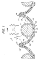
- Fig. 1 is an enlarged sectional view of part of a photovoltaic apparatus 1 according to an embodiment of the present invention.
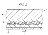
- Fig. 2 is a sectional view showing the structure of the photovoltaic apparatus 1
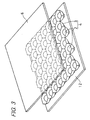
- Fig. 3 is an exploded perspective view of the photovoltaic apparatus 1 of Fig. 2 .
- the photovoltaic apparatus 1 has the following basic structure.
- An assembly 4 of a plurality of generally spherical photoelectric conversion elements 2 and a support 3 that is mounted with the photoelectric conversion elements 2 is buried in a filler layer 5 made of a transparent synthetic resin material such as PVB (poly(vinyl butyral)) or EVA (ethylene vinyl acetate).
- PVB poly(vinyl butyral)
- EVA ethylene vinyl acetate
- a transparent protective sheet 6 made of polycarbonate or the like is provided on the light source (e.g., sunlight) side of the filler layer 5 and is fixed to it.
- a waterproof back sheet 12 is fixed to the surface of the filler layer 5 on the opposite side to the protective sheet 6 ⁇ bottom side in Fig. 2 ). As such, the photovoltaic apparatus 1 assumes, as a whole, a flat-plate shape.
- Each photoelectric conversion element 2 has a first semiconductor layer 7 and a second semiconductor layer 8 located outside the first semiconductor layer 7. An opening 9 is formed on the second semiconductor layer 8. A portion 10 (a bottom portion in Fig. 1 ) of the first semiconductor layer 7 is exposed through the opening 9. When light 11 is applied from above in Fig. 1 , photoelectromotive force is generated between the first semiconductor layer 7 and the second semiconductor layer 8 of the photoelectric conversion element 2.
- the support 3 is configured in such a manner that an insulator 15 is sandwiched between a first conductor 13 and a second conductor 14. That is; the first conductor 13 and the second conductor 14 are electrically insulated from each other by the insulator 15.
- Each of the first conductor 13 and the second conductor 14 may be a sheet of aluminum foil or a sheet of another metal.
- the insulator 15 may be made of a synthetic resin material such as polyimide or some other insulative material.
- a plurality of recesses 17 are arranged adjacent to each other. The inside surfaces of the recesses 17 are the surface of the first conductor 13.
- the photoelectric conversion elements 2 are provided at the bottoms of the respective recesses 17.
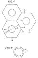
- Fig. 4 is a plan view of part of the support 3.
- openings 18 of the recesses 17 assume polygons. In this embodiment, they assume a honeycomb shape, that is, regular hexagons. According to another embodiment of the invention, the opening 18 of each recess 17 assumes another kind of polygon having three or more apices.
- the length W1 (see Fig. 4 ) of each opening 18 is 2 mm, for example.
- the openings 18 which are adjacent to each other are continuous; that is, the recesses 17 are connected to each other by inverted-U-shaped bent portions 19 (see Fig. 1 ).
- This structure makes it possible to accommodate as many recesses 17 as possible in the area that is opposed to the light 11, as well as to cause the inside surfaces of the recesses 17 (i.e., the surface of the first conductor 13) to reflect incident light and guide resulting reflection light to the respective photoelectric conversion elements 2. Therefore, this structure provides a large light-gathering ratio.
- Each recess 17 narrows toward the bottom and assumes a parabolic cross-section, for example.
- the first semiconductor layer 7 of the photoelectric conversion element 2 is electrically connected to the second conductor 14 of the support 3 via a connecting portion 21.
- the second semiconductor layer 8 of the photoelectric conversion element 2 is electrically connected to the first conductor 13 of the support 3.
- Fig. 5 is a sectional view of a photoelectric conversion element 31 that is a version of each photoelectric conversion element 2 before being mounted on the support 3.
- the sectional structure of the photoelectric conversion element 31 in Fig. 5 is similar to that of each photoelectric conversion element 2 shown in Fig. 1 .
- a spherical first semiconductor layer 7 is made of n-type silicon, which may be amorphous, single-crystal, or polycrystalline silicon.
- a second semiconductor layer 8 located outside the first semiconductor layer 7 is made of p-type silicon, which may also be amorphous, single-crystal, or polycrystalline silicon.
- the optical band gap of the second semiconductor layer 8 is set wider than that of the first semiconductor layer 7 (e.g., the second semiconductor layer 8 is made of p-type a-SiC), wide gap window action can be attained.
- the first semiconductor layer 7 shown in Fig. 5 is made of a direct gap semiconductor that is a semiconductor selected from the group consisting of InAs, CuInSe 2 , Cu(InGa)Se 2 , CuInS, GaAs, InGaP, and CdTe that exhibit n-type conductivity.
- the second semiconductor layer 8 is formed on the first semiconductor layer 7 made of such a direct gap semiconductor.
- the second semiconductor layer 8 is made of a semiconductor selected from the group consisting of AlGaAs, CuInSe 2 , Cu(InGa)Se 2 , GaAs, AlGaP, and CdTe that exhibit p-type conductivity and compound semiconductors similar to those.
- a pn junction structure is formed in this manner.
- a pin junction structure may be formed by forming an i-type semiconductor layer 69 between a first semiconductor layer 68 and the second semiconductor layer 70 (described later; see Fig. 15 ).
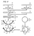
- Fig. 6 is a sectional view showing a method for producing the assembly 4 of the photoelectric conversion elements 2 and the support 3.
- the photoelectric conversion elements 2 are cut as shown in Fig. 6 .
- a portion 10 of the first semiconductor layer 7 is exposed through an opening 9 of the second semiconductor layer 8.
- the opening 9 has such a shape as would be obtained by cutting the photoelectric conversion elements 31 by a plane, and has a central angle ⁇ 1 that is less than 180°.
- the central angle ⁇ 1 may be in a range of 45° to 90°, for example.
- the central angle ⁇ 1 be in a range of 60° to 90°.
- the outer diameter D1 of each photoelectric conversion element 31 may be in a range of 0.5 mm to 2.0 mm, for example. It is preferable that the outer diameter D1 be in a range of 0.8 mm to 1.2 mm.
- symbol D2 represents the inner diameter of the opening 9.
- the light-gathering ratio x S1/S2 is in a range of 2 to 8, where S1 is the opening area of each recess 17 of the support 3 and S2 is the area of a cross-section including its center, of each photoelectric conversion element 2. It is preferable that the light-gathering ratio x be in a range of 4 to 6.
- Fig. 7 is a sectional view showing a process for forming the opening 9 by cutting each spherical photoelectric conversion element 31. While the top portion of each of spherical photoelectric conversion elements 31 is vacuum-attracted by an attraction pad 34, the spherical photoelectric conversion elements 31 are ground by an endless-belt-shaped abrasive 35. The abrasive 35 is wound on rollers 36 and 37 and is thereby driven rotationally.
- connection holes 39 are formed therein.
- the inner diameter D3 of each connection hole 39 is set smaller than the outer diameter D1 of each photoelectric conversion element 2 and greater than the inner diameter D2 of the opening 9 of the second semiconductor layer 8 (D1 > D3 > D2).
- a thin-plate-shaped insulator 15 is prepared and connection holes 40 are formed therein.
- the inner diameter D4 of each connection hole 40 is set smaller than the inner diameter D2 of the opening 9 of each photoelectric conversion element 2 (D2 > D4).
- the first conductor 13 having the connection holes 39 is laid on and bonded to the insulator 15 having the connection holes 40, whereby the first conductor 13 and the insulator 15 are integrated with each other.
- Each pair of connection holes 39 and 40 shares a common axial line.
- the resulting structure is laid on and bonded to a second conductor 14, whereby they are integrated with each other to produce a flat support 3a.
- the first conductor 13 having the connection holes 39, the insulator 15 having the connection holes 40, and the second conductor 14 are laid one on another and bonded to each other at one time, whereby they are integrated with each other.
- Each of the first conductor 13, the second conductor 14, and the insulator 15 may have a thickness of 60 ⁇ m, for example.
- the portion around the opening 9 of each photoelectric conversion element 2 fits into the connection hole 39 and is opposed to the connection hole 40 of the insulator 15. Alternatively, the portion around the opening 9 may be placed on the first conductor 13 so as to be opposed to the connection hole 39.
- Fig. 1 That portion of the outer surface of the second semiconductor layer 8 of each photoelectric conversion element 2 which is located above the opening 9 in Fig. 1 and surrounds the opening 9 is electrically connected to that portion of the first conductor 13 of the support 3a (or 3) which is in the vicinity of the connection hole 39, that is, the inner circumferential face of the connection hole 39 or that portion of the first conductor 13 which is in the vicinity of and surrounds the connection hole 39.
- a connecting portion 44 (see Fig. 1 ) where the outer surface of the second semiconductor layer 8 is connected to the first conductor 13 is located on the opposite side (above in Fig.
- the connecting portion 44 is parallel with the bottom surface of the photoelectric conversion element 2 containing the opening 9 and is closer to the opening 9 (i.e., lower in Fig. 1 ) than an imaginary plane 47 passing through the center 46 of the photoelectric conversion element 2 is.
- a resulting support 3 may have a height H1 of about 1 mm, for example.
- the step of electrically connecting the first semiconductor layers 7 to the second conductor 14 and the step of electrically connecting the second semiconductor layers 8 to the first conductor 13 may be performed either sequentially (either step may be performed first) or simultaneously.
- the photoelectric conversion elements 2 each having the opening 9 are accommodated in the respective recesses 17 thus formed.
- the support 3 is produced in the following manner. After the 3-layer structure of the first conductor 13, the insulator 15, and the second conductor 14 is plastically deformed so as to form recesses 17, connection holes 39 and 40 are formed in the first conductor 13 and the insulator 15, respectively, by using two kinds of laser light.
- Fig. 8 is a simplified perspective view showing a process for putting the photoelectric conversion elements 2 in the respective recesses 17 of the support 3.
- a set of photoelectric conversion elements 2 produced by cutting photoelectric conversion elements 31 in a state that they are vacuum-attracted by the attraction pads 34 is transported with the openings 9 kept down and put in respective recesses 17 of the support 3.
- 100 attraction pads 34 are arranged in line.
- the support 3 is moved in a direction 42 by a distance that is equal to one pitch of the recesses 17, another set of photoelectric conversion elements 2 is put in new recesses 17 by using the attraction pads 34 in the same manner as described above.
- Photoelectric conversion elements 2 are put in all the recesses 17 by repeating the above operation. Then, the operation of electrically connecting each photoelectric conversion element 2 to the support 3 is performed at the bottom of each recess 17.
- the first semiconductor layer 7 of each photoelectric conversion element 2 is exposed through the opening 9 and is electrically connected to the connecting portion 21 through the connection hole 40 of the second conductor 14.
- the portion, above the opening 9, of the outer surface of the second semiconductor layer 8 of each photoelectric conversion element 2 is electrically connected to that portion of the first conductor 13 which is in the vicinity of the connection hole 39.
- the first semiconductor layer 7 and the second semiconductor layer 8 of each photoelectric conversion element 2 may be connected electrically to the second conductor 14 and the first conductor 13, respectively, by using laser light (formation of an eutectic), conductive paste, orametalbump. Inthismanner, the electrical connection is made without using lead-containing solder, which is preferable in terms of the environmental protection.
- Fig. 9 is a perspective view showing how assemblies 4 and 4b of the photoelectric conversion elements 2 and the support 3 are connected to each other.
- the assemblies 4 and 4b are electrically connected to each other at their flat peripheral portions 61 and 61b extending outward.
- Fig. 10 is an exploded sectional view of the peripheral portions 61 and 61b and their vicinities of the assemblies 4 and 4b shown in Fig. 9 .
- the second conductor 14 of the support 3b of the one assembly 4b is laid on, electrically connected to, and fixed to the first conductor 13 of the support 3 of the other assembly 4. In this manner, photoelectromotive forces, generated by the photoelectric conversion elements 2, of the assemblies 4, 4b, ... are connected to each other in series, whereby a desired high voltage can be output.
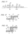
- Fig. 11 is a simplified side view showing how assemblies 4, 4b, and 4c are electrically connected to each other.
- the peripheral portion 61b of the assembly 4b is laid on and electrically connected to the peripheral portion 61 of the assembly 4 in the above-described manner.
- the peripheral portion 61c of the assembly 4c is laid on and electrically connected to the peripheral portion 61b1 (located on the opposite side to the peripheral portion 61b) of the assembly 4b.
- the one peripheral portion 61b of the assembly 4b is located above the peripheral portion 61 of the assembly 4 and the other peripheral portion 61b1 of the assembly 4b is located below the peripheral portion 61c of the assembly 4c.
- the assemblies are connected to each other in such a manner that the two peripheral portions of each assembly are located above and below the two adjacent assemblies, respectively, to thereby form a two-step structure.
- the length L61 of overlap, in the right-left direction in Fig. 11 , between the peripheral portions 61 and 61b and between the peripheral portions 61b1 and 61c may be set at 1 mm, for example.
- Fig. 12 is a sectional view showing an electrical connection structure of assemblies 4 and 4b that are adjacent to each other according to another embodiment of the invention.
- the peripheral portion 61 of the one assembly 4 projects upward and the peripheral portion 61b of the other assembly 4b projects downward.
- the second conductor 14 of the peripheral portion 61 is electrically connected to the first conductor 13 of the peripheral portion 61b.
- Fig. 13 is a sectional view showing an electrical connection structure of assemblies 4 and 4b that are adjacent to each other according to still another embodiment of the invention.
- This embodiment is similar to the embodiment of Fig. 12 and is different from the latter in that the first conductor 13 of the peripheral portion 61 (projecting upward) of the assembly 4 is electrically connected to the second conductor 14 of the peripheral portion 61b (projecting downward) of the assembly 4b.
- the connection structures of Figs. 12 and 13 make it possible to make the recesses 17 of the supports 3 and 3b closer to each other and thereby arrange as many recesses 17 and photoelectric conversion elements 2 as possible in a limited area.
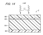
- Fig. 14 is a sectional view of part of a photoelectric conversion element 2 according to another embodiment of the invention.
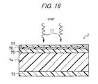
- each semiconductor layer is drawn as having a flat shape (developed in the circumferential direction), actually the semiconductor layers are laid one on another outward (upward in Figs. 14-16 ) in the radial direction so as to have spherical surfaces.
- an n-type microcrystalline ( ⁇ c) silicon layer 63, an n-type polysilicon layer 64, a p-type a-SiC layer 65, and a p-type microcrystalline SiC layer 66 are laid one on another outward in the radial direction.
- the structures of the photoelectric conversion elements 2 of Figs. 14-16 each having a pn junction are summarized in Table 1.
- Fig. 15 is a sectional view of the photoelectric conversion element 2 according to still another embodiment of the invention.
- the details of semiconductor layers 68-70 are as shown in Table 1.
- the semiconductor layer 68 may be made of n-type single-crystal or polycrystalline silicon.
- Fig. 16 is a sectional view of the photoelectric conversion element 2 according to yet another embodiment of the invention.
- the details of semiconductor layers 73-77 are as shown in Table 1.
- the semiconductor layers 73 and 74 in Fig. 16 are made of n-type single-crystal silicon.
- the semiconductor layer 74 may be made of i-type microcrystalline silicon.
- the photoelectric conversion element 2 may have structures other than described above.
- the support 3 may be replaced by another type of support that is produced by forming a structure having recesses by molding (e. g. , injection-molding) an insulative synthetic resin material (e.g., polycarbonate), for example, and plating a conductive material such as Ni on its surfaces to form first and second conductors.
- the first and second conductors may be made of aluminum foil, for example.
- they may be formed by Cr plating or Ag plating.
- they may be formed by evaporating or sputtering a metal of Ni, Cr, Al, Ag, or the like.
- a coating may be formed on the first conductor, and the coating may be made of a metal (formed by plating or the like) or a synthetic resin.
- pin junction includes a structure that n, i and p-type semiconductor layers are formed on an approximately spherical photoelectric conversion element 2 so as to be arranged inward or outward in this order.
- Spherical semiconductor particles manufactured according to the invention are photoelectric conversion elements.
- the above-described photovoltaic apparatus 1 can be constructed by using photoelectric conversion elements 2 thus manufactured.
Landscapes
- Chemical & Material Sciences (AREA)
- Engineering & Computer Science (AREA)
- Crystallography & Structural Chemistry (AREA)
- Materials Engineering (AREA)
- Metallurgy (AREA)
- Organic Chemistry (AREA)
- Physics & Mathematics (AREA)
- Geometry (AREA)
- Mechanical Engineering (AREA)
- Photovoltaic Devices (AREA)
- Silicon Compounds (AREA)
Abstract
Description
- The present invention relates to a photovoltaic apparatus and to a mass-producing apparatus for mass-producing spherical semiconductor particles, suitable for manufacture of photovoltaic apparatus and the like.
- In the disclosure herein described, the term "pin junction" is to be construed as including a structure that n-, I- and p-type semiconductor layers are formed on an approximately spherical photoelectric conversion element so as to be arranged in this order outward from the inside of the approximately spherical photoelectric conversion element or inward from the outside.
- A typical related art technique provides a photovoltaic apparatus comprising a photoelectric conversion element composed of a crystal silicon semiconductor wafer. The related art photovoltaic apparatus is of cost expenditure because the step for producing a crystal is complex. Furthermore, the step for manufacturing a semiconductor wafer is not only complex because it includes cutting of a bulk single crystal, slicing, and polishing, but also the step is wasteful because crystal waste produced by the cutting, slicing, polishing etc. amounts to about 50% by volume or more of the original bulk single crystal.
- Another related art technique provides a photovoltaic apparatus comprising a photoelectric conversion element composed of an amorphous silicon (abbreviated as "a-Si") thin film, which solves the above-mentioned problems. Since a thin-film photoelectric conversion layer is formed by the plasma CVD (chemical vapor deposition) method, this related art photovoltaic apparatus has advantages that the steps which are conventionally required, such as cutting of a bulk single crystal, slicing, and polishing, are not necessary and that a deposited film can be used in its entirety as device active layers. The amorphous silicon photovoltaic apparatus, however, has a drawback that the semiconductor has a number of crystal defects (i.e., gap states) inside the semiconductor due to the amorphous structure, the amorphous silicon solar battery has a problem that the photoelectric conversion efficiency decreases due to a photo-induced deterioration phenomenon. To solve this problem, conventionally, a technique of inactivating crystal defects by applying hydrogenation treatment has been developed, whereby the manufacture of such electronic devices as an amorphous silicon solar battery has been realized.
- Even such a treatment, however, cannot entirely eliminate the adverse effects of crystal defects, and for example, the amorphous silicon solar battery still has a weak point that the photoelectric conversion efficiency decreases by 15% to 25%.
- A recently developed technique for suppressing the photo-induced deterioration has realized a stack-type solar battery in which a photoelectrically active i-type layer is made extremely thin and 2-junction or 3-junction solar cells are used, and has succeeded in suppressing the photo-induced deterioration to about 10%. It has become apparent that the degree of photo-induced deterioration decreases when the operation temperature of solar cells is high. Although a module technique in which solar cells are caused to operate in such a condition is now being developed, it does not satisfy all the requirements and further improvements are required.
- Still another related art technique in which the above problem is eliminated is disclosed in Japanese Examined Patent Publication
JP-B2 7-54855 (1995 - In this related art technique, to reduce the costs by decreasing the used amount of high-purity silicon, it is necessary to decrease the average thickness of the entire device by decreasing the outer diameter of the particles. To increase the conversion efficiency, it is necessary to enlarge the light-receiving surface, and to this end, it is necessary to arrange the particles closer to each other. In summary, a number of particles having a small outer diameter need to be arranged densely and connected to the sheets of aluminum foil. This makes complex the step of connecting the particles to the sheets of aluminum foil, with the result that a sufficient cost reduction is not achieved.
- Such spherical semiconductor particles are required in order to manufacture a solar array such as one disclosed in
JP-B2 7-54855 - As disclosed in
U.S. Patent No. 5,012,619 , for example, such spherical particles are manufactured in such a manner that a solid-state material is crushed into particles having irregular outer shapes, resulting particles are put in a cylinder that is provided with a lining for grinding, and a gas eddy flow is formed in the cylinder to thereby collide the particles with the lining or with each other. - This related art technique requires much time and labor to manufacture spherical semiconductor particles and hence is inferior in cost reduction aspect.
- Yet another related art technique is disclosed in Japanese Unexamined Patent Publication
JP-A 8-239298 (1996 - It is noted that American patent publications
US 4 521 640 andUS 5 466 301 disclose a photovoltaic apparatus comprising a plurality of semiconductor spheres arranged in a support having a generally flat conductor layer being electrically connected to the outside layer of the semiconductor spheres. - An object of the present invention is to provide a highly reliable, highly efficient photovoltaic apparatus that can be mass-produced easily while the used amount of semiconductor material such as high-purity silicon is decreased, that is, a highly reliable, high-efficiency photovoltaic apparatus that can be manufactured at low costs with smaller amounts of consumption of resources and energy.
- Another object of the invention is to provide an apparatus capable of mass-producing spherical semiconductor particles easily by simple manipulations.
- A first aspect of the invention provides a photovoltaic apparatus according to
claim 1. - According to the invention, the approximately spherical photoelectric conversion elements are disposed in the respective recesses of the support and the inside surfaces of the respective recesses are constituted by the first conductor or the coating formed on the first conductor. Therefore, external light such as sunlight is directly applied to each of the photoelectric conversion elements as well as after being reflected by the part of the first conductor or coating formed on the first conductor which is the inside surface of the recess.
- Since the photoelectric conversion elements are disposed in the respective recesses, intervals are formed in between, that is, their arrangement is not dense. However, the number of photoelectric conversion elements used is decreased, with the result that the used amount of high-purity material (e.g., silicon) of the photoelectric conversion elements can be reduced and the step of connecting the photoelectric conversion elements to the conductors of the support can be made easier.
- Further, the recesses are arranged adj acent to each other, whereby external light is reflected by the inside surfaces of the recesses and then applied to the photoelectric conversion elements. Therefore, external light can be efficiently used for generation of photoelectromotive force by the photoelectric conversion elements. Accordingly it is achieved to maximize the electric power generation amount per unit area opposed to a light source of the photoelectric conversion elements.
- The photoelectric conversion elements may be made of a single-crystal, polycrystalline, or amorphous material and may be made of a silicon material, a compound semiconductor material, or the like. The photoelectric conversion elements may have a pn structure, a pin structure, a Schottky barrier structure, a MIS (metal-insulator-semiconductor) structure, a homo junction structure, a heterojunction structure, or the like.
- The inside first semiconductor layer is partially exposed through the opening of the outside second semiconductor layer, which makes it possible to take out photoelectromotive force that is generated between the first and second semiconductor layers during application of light. The second semiconductor layers of the respective photoelectric conversion elements disposed in the respective recesses of the support are electrically connected to the first conductor of the support. The exposed portions of the inside first semiconductor layers of the respective photoelectric conversion elements are electrically connected to the second conductor which is formed on the first conductor with the insulator interposed in between. In a structure in which the first conductor and the second conductor extend to form a plane, the photoelectric conversion elements are connected to each other in parallel with the first and second conductors and can produce a large current.
- The photoelectric conversion element may either be a complete sphere or have an outer surface that is approximately a complete spherical surface. The first semiconductor layer may be solid and have an approximately spherical shape. Alternatively, the first semiconductor layer may be formed on the outer surface of a core that is prepared in advance. As a further alternative, the approximately spherical first semiconductor layer may have a hollow central portion.
- In the invention it is preferable that the photoelectric conversion elements have an outer diameter of 0.5 mm to 2.0 mm.
- According to the invention, the photoelectric conversion elements may have an outer diameter of 0.5 mm to 2.0 mm, preferably of 0.8 to 1.2 mm, more preferably of about 1. 0 mm. This makes it possible to sufficiently reduce the used amount of material such as high-purity silicon and to maximize the electric power generation amount. Further, the spherical photoelectric conversion elements can be handled easily during manufacture and the productivity can be increased.
- In the invention it is preferable that the opening of the second semiconductor layer has a central angle θ1 of 45° to 90°.
- By setting the central angle θ1 at 45° to 90°, preferably at 60° to 90°, the amounts of those parts of the first and second semiconductor layers which are discarded to form the opening can be reduced, that is, the loss of material can be reduced. Further, setting the central angle θ1 in such a range allows the opening to have a sufficient area for the electrical connection between the first semiconductor layer and the second conductor of the support.
- In the invention it is preferable that the recesses of the support have respective openings of a polygon (e.g., honeycomb polygon) of which ones adjacent to each other are continuous, that each of the recesses narrows toward a bottom thereof, and the first semiconductor layer and second semiconductor layer of each of the photoelectric conversion elements are electrically connected to the second conductor and the first conductor, respectively, at the bottom or in a vicinity thereof of the recess.
- In the invention it is preferable that the first conductor is provided with a circular first connection hole formed at the bottom or in a vicinity thereof of the recess and the insulator is provided with a circular second connection hole having a common axial line with the first connection hole, that a portion of the photoelectric conversion element in a vicinity of the opening of the second semiconductor layer fits in the first connection hole and an outer surface portion above the opening of the second semiconductor layer is electrically connected to an end face of the first connection hole of the first conductor or to a portion thereof in the vicinity of the end face, and that the exposed portion of the first semiconductor layer of the photoelectric conversion element is electrically connected to the second conductor through the second connection hole.
- In the invention it is preferable that an outer diameter D1 of the photoelectric conversion elements, an inner diameter D2 of the openings of the second semiconductor layers, and an inner diameter D3 of the first connection holes, and an inner diameter D4 of the second connection holes satisfy a relationship D1 > D3 > D2 > D4.
- According to the invention, a portion of the photoelectric conversion element in the vicinity of the opening fits in the first connection hole of the first conductor and the exposed portion of the first semiconductor layer of the photoelectric conversion element is electrically connected to the second conductor through the second connection hole of the insulator of the support, the first conductor and the second conductor of the support can easily be connected electrically to the second semiconductor layer and the first semiconductor layer, respectively, of the photoelectric conversion element.
- As for the electrical connection between the second semiconductor layer and the first conductor, a portion, above the opening, of the outer surface of the second semiconductor layer is electrically connected to the end face of the first connection hole and/or a portion of the first conductor in the vicinity of the end face, that is, the inner circumferential face of the first connection hole and/or a portion of the first conductor in the vicinity of and surrounding the first connection hole (see
Fig. 1 ). - For example, each projection of the second conductor formed by elastic deformation may be inserted through the second connection hole and electrically connected to the portion of the first semiconductor layer that is exposed through the opening. Alternatively, the portion of the first semiconductor layer that is exposed through the opening may be connected to the second conductor with conductive paste provided in the second connection hole or via a conductive bump such as a metal bump.
- Setting the outer diameter D1 and the inner diameters D2-D4 so as to satisfy the above inequality enables reliable electrical connection without causing undesired short-circuiting.
- In the invention it is preferable that a light-gathering ratio x which equals to S1/S2 is selected to be in a range of 2 to 8, wherein SI is an opening area of each of the recesses of the support and S2 is an area of a cross-section of the photoelectric conversion elements including a center thereof.
- A second aspect of the invention provides a photovoltaic apparatus according to
claim 8. - A third aspect of the invention provides a photovoltaic apparatus according to
claim 9. - For example, the openings of the respective recesses of the support assume honeycomb polygons such as hexagon. Each recess narrows toward its bottom, and a photoelectric conversion element is disposed at the bottom of each recess. Each photoelectric conversion element is electrically connected to the conductors of the support at the bottom or its neighborhood of the recess. Since the openings of the respective recesses assume polygons and are continuous with each other, all the light received by all the surface of the support opposed to a light source (e.g., sunlight) excluding the areas of the photoelectric conversion elements can be applied to the photoelectric conversion elements. Therefore, what is called a light-gathering-type photoelectric conversion element can be realized in which the light-gathering ratio x = S1/S2 is set at 2 to 8, for example (preferably 4 to 6). This makes it possible to increase the intervals between the photoelectric conversion elements, decrease the number of photoelectric conversion elements, and simplify the step of electrically connecting the photoelectric conversion elements to the support. Therefore, the used amount of high-purity semiconductor as a material of the photoelectric conversion elements can be reduced and the invention can be practiced inexpensively. Having a relatively simple structure, the support is superior in productivity and can be manufactured easily.
- An experiment conducted by the present inventor shows that when a photovoltaic apparatus according to the invention in which the approximately spherical silicon photoelectric conversion elements have an outer diameter of 800 µm to 1,000 µm and the light-gathering ratio x is set at 4-6 is converted into an imaginary flat plate that uses the same weight of silicon as the silicon that constitutes all the photoelectric conversion elements of the photovoltaic apparatus and that has the same area as the area of a projection of the photovoltaic apparatus onto a plane perpendicular to light coming from a light source, the imaginary flat plate has a thickness of about 90 µm to 120 µm. This means that the amount of silicon that is used for generating an electric power of 1 W is as small as 2 g, which is an epoch-making conclusion. In the above-described first prior art technique using photoelectric conversion elements formed on a single-crystal silicon semiconductor wafer, the silicon single crystal is as thick as 350 µm to 500 µm and the thickness amounts to about 1 mm when the slice loss is included. Therefore, in the first prior art technique, the amount of silicon that is used for generating an electric power of 1 W is about 15 to 20 g. It is understood that the invention can make the used amount of silicon much smaller than in the first prior art technique.
- When the light-gathering ratio x is set larger than 8, the number of necessary photoelectric conversion elements can be decreased and the amount of silicon used for generating an electric power of 1 W could further be reduced. However, in practice, as the light-gathering ratio x increases, the light-gathering efficiency which is the ratio of optical energy absorbed by the photoelectric conversion elements to that incident on the recesses becomes smaller and the performance of the photovoltaic apparatus lowers accordingly.
- By setting, as described above, the outer diameter of each photoelectric conversion element at 0.5 mm to 2.0 mm (preferably 0.8 mm to 1.2 mm) and setting the light-gathering ratio x at 2 to 8 (preferably 4 to 6), the number of photoelectric conversion elements can be decreased, the amount of silicon used for generating an electric power of 1 W can be reduced, and the step of electrically connecting the photoelectric conversion elements to the support can further be simplified. As such, the combination of the values of the outer diameter of each photoelectric conversion element and the light gathering ratio x is important in decreasing the number of photoelectric conversion elements and reducing the amount of silicon used for generating an electric power of 1 W.
- When the outer diameter of each photoelectric conversion element is smaller than 0.5 mm, the number of necessary photoelectric conversion elements becomes unduly large though the used amount of silicon decreases. When the outer diameter of each photoelectric conversion element is greater than 2 mm, the used amount of silicon becomes unduly large though the number of necessary photoelectric conversion elements decreases.
- When the light-gathering ratio is smaller than 2, the used amount of silicon cannot be reduced sufficiently. When the light-gathering ratio is greater than 8, the light-gathering efficiency becomes smaller than 80%, for example, and the performance lowers accordingly. By setting the light-gathering ratio x in the proper range, the invention makes it possible to make the light-gathering efficiency greater than 80% or even 90%.
- According to the invention, by setting the values of the outer diameter of each photoelectric conversion element and the light-gathering ratio x in the above-mentioned ranges, such a remarkable advantage is achieved that both of the number of necessary photoelectric conversion elements and the amount of silicon to be used for generating an electric power of 1W can greatly be decreased to 1/5 to 1/10 of those in the third prior art technique.
- In a photovoltaic apparatus in which amorphous silicon photoelectric conversion elements are used and light is gathered at a light-gathering ratio in the above-mentioned range, the temperature of the photoelectric conversion elements can be increased to 40°C to 80°C, which is higher than in the case of using an amorphous silicon, thin-plate photoelectric conversion element. This makes it possible to suppress deterioration of the amorphous silicon photoelectric conversion element and to thereby elongate the life of the photovoltaic apparatus.
- In the invention it is preferable that the photoelectric conversion elements have a pn junction in such a manner that the second semiconductor layer of one conductivity type having a wider optical band gap than the first semiconductor layer having the other conductivity type does is formed outside the first semiconductor layer {see
Fig. 14 }. - In the invention it is preferable that the photoelectric conversion elements have a pin junction in such a manner that the first semiconductor layer having one conductivity type, an amorphous intrinsic semiconductor layer, and an amorphous second semiconductor layer of the other conductivity type having a wider optical band gap than the first semiconductor layer does are arranged outward in this order (see
Figs. 15 and16 ). - In the invention it is preferable that the first semiconductor layer and the second semiconductor layer are made of n-type silicon and p-type amorphous SiC, respectively.
- In the invention it is preferable that the n-type silicon of which the first semiconductor layer is made is n-type single-crystal silicon or n-typemicrocrystalline (µc) silicon.
- In the invention it is preferable that the first semiconductor layer is a direct gap semiconductor layer.
- In the invention it is preferable that the direct gap semiconductor layer is made of a semiconductor selected from the group consisting of InAs, GaSb, CuInSe2, Cu(InGa)Se2, CuInS, GaAs, InGaP, and CdTe.
- According to the invention, employing, as the inside first semiconductor layer, a direct gap semiconductor which easily absorbs light makes it possible to obtain sufficiently high electron and hole transition probabilities, which also contributes to increase of the photoelectric conversion efficiency.
- In the invention it is preferable that a plurality of the supports each having peripheral portions extending outward are arranged adjacent to each other, and that part of the first conductor in the peripheral portion of one support of each pair of supports adj acent to each other and part of the second conductor in the peripheral portion of the other are laid one on another and electrically connected to each other.
- In the invention it is preferable that the peripheral portion has upward projections or downward projections, and that the upward projection or downward projection of one support of each pair of supports adjacent to each other and the upward projection or downward projection of the other are brought into contact with and electrically connected to each other.
- According to the invention, where part of the first conductor in a peripheral portion of one support of each pair of supports adjacent to each other among a plurality of supports mounted with photoelectric conversion elements and part of the second conductor in a peripheral portion of the other are laid one on another and electrically connected to each other, photoelectromotive forces, generated by the photoelectric conversion elements, of the respective supports are connected to each other in series. This makes it possible to output a desired high voltage.
- According to the invention, where an upward projection and a downward projection, upward projections, or downward projections of peripheral portions of each pair of supports adjacent to each other are electrically connected to each other (see
Figs. 12 and 13 ), the recesses of each support can be made closer to each other and as many recesses and photoelectric conversion elements as possible can be arranged in a limited area. - The invention makes it possible to greatly reduce the used amount of photoelectric conversion element material (in particular, expensive silicon) and to simplify the step of connecting the photoelectric conversion elements to the support by decreasing the number of photoelectric conversion elements, to thereby increase the productivity and reduce the cost. In particular, the use of the photoelectric conversion elements according to the invention makes it possible to realize a manufacturing method capable of saving resources and energy. Sunlight or the like is reflected by the surface of the first conductor or a coating formed thereon that constitutes the inside surface of each recess of the support and resulting reflection light shines on the photoelectric conversion element. In this manner, incident light can be utilized effectively. The first conductor or a coating formed thereon serves to not only reflect incident light but also guide currents (the first conductor is connected to the second semiconductor layers of the respective photoelectric conversion elements). Having a simple structure, the support is superior in productivity.
- In particular, by setting the outer diameter of each photoelectric conversion element at 0. 5 mm to 2.0 mm (preferably 0.8 mm to 1.2 mm) and the light-gathering ratio x at 2 to 8 (preferably 4 to 6), the inventionprovides a remarkable advantage that both of the amount of silicon to be used for generating an electric power of 1W and the number of necessary photoelectric conversion elements can greatly be decreased to 1/5 to 1/10 of those in the third prior art technique. Reducing the used amount of silicon makes it possible to realize a photovoltaic apparatus at a low cost. Decreasing the number of photoelectric conversion elements and thereby simplifying the step of electrically connecting the photoelectric conversion elements to the support increase the productivity, which also contributes to realization of a low-cost photovoltaic apparatus.
- Therefore, the invention makes it possible to provide a highly reliable, highly efficient photovoltaic apparatus.
- A pn or pin junction is formed by setting the optical band gap of the outside amorphous second semiconductor layer wider than that of the center-side first semiconductor layer. With this measure, light is not much absorbed by the light-incidence-side second semiconductor layer made of a window material, whereby the recombination rate of the surface layer is decreased and wide gap window action is attained. The energy conversion efficiency can be increased as a result of those effects.
- Inserting a microcrystalline (µc) semiconductor layer having high conductivity between the center-side first semiconductor layer and the outside pin junction layer makes it possible to increase the energy conversion efficiency.
- The invention also makes it possible to increase the energy conversion efficiency by using a direct gap first semiconductor layer.
- Further, the invention facilitates manufacture of photoelectric conversion elements.
- The invention makes it possible to mass-produce spherical semiconductor particles having uniform particle diameters by a simple operation by dropping, from the nozzle, a semiconductor that has been melted in the crucible and vibrating the molten semiconductor. Particles thus produced can easily be converted into single-crystal or polycrystalline particles in a vapor phase. And each crystalline semiconductor particle can easily be formed with a surface layer though impurity doping.
- Other and further objects, features, and advantages of the invention will be more explicit from the following detailed description taken with reference to the drawings wherein:
-
Fig. 1 is an enlarged sectional view of part of aphotovoltaic apparatus 1 according to an embodiment of the present invention; -
Fig. 2 is a sectional view showing the structure of thephotovoltaic apparatus 1; -
Fig. 3 is an exploded perspective view of thephotovoltaic apparatus 1 ofFig. 2 ; -
Fig. 4 is a plan view of part of asupport 3; -
Fig. 5 is a sectional view of aphotoelectric conversion element 31 that is a version of eachphotoelectric conversion element 2 before being mounted on thesupport 3; -
Fig. 6 is a sectional view showing a method for producing anassembly 4 of thephotoelectric conversion elements 2 and thesupport 3; -
Fig. 7 is a sectional view showing a process for forming an opening 32 by cutting each sphericalphotoelectric conversion element 31; -
Fig. 8 is a simplified perspective view showing a process for placing thephotoelectric conversion elements 2 intorespective recesses 17 of thesupport 3; -
Fig. 9 is a perspective view showing howassemblies photoelectric conversion elements 2 and thesupport 3 are connected to each other; -
Fig. 10 is an exploded sectional view ofperipheral portions 61 and Sib and their vicinities of theassemblies Fig. 9 ; -
Fig. 11 is a simplified side view showing howassemblies -
Fig. 12 is a sectional view showing an electrical connection structure ofassemblies -
Fig. 13 is a sectional view showing an electrical connection structure ofassemblies -
Fig. 14 is a sectional view of part of aphotoelectric conversion element 2 according to another embodiment of the invention; -
Fig. 15 is a sectional view of part of aphotoelectric conversion element 2 according to still another embodiment of the invention; and -
Fig. 16 is a sectional view of part of aphotoelectric conversion element 2 according to yet another embodiment of the invention. - Now referring to the drawings, preferred embodiments of the invention are described below.
-
Fig. 1 is an enlarged sectional view of part of aphotovoltaic apparatus 1 according to an embodiment of the present invention.Fig. 2 is a sectional view showing the structure of thephotovoltaic apparatus 1,Fig. 3 is an exploded perspective view of thephotovoltaic apparatus 1 ofFig. 2 . Thephotovoltaic apparatus 1 has the following basic structure. Anassembly 4 of a plurality of generally sphericalphotoelectric conversion elements 2 and asupport 3 that is mounted with thephotoelectric conversion elements 2 is buried in afiller layer 5 made of a transparent synthetic resin material such as PVB (poly(vinyl butyral)) or EVA (ethylene vinyl acetate). A transparentprotective sheet 6 made of polycarbonate or the like is provided on the light source (e.g., sunlight) side of thefiller layer 5 and is fixed to it. Awaterproof back sheet 12 is fixed to the surface of thefiller layer 5 on the opposite side to the protective sheet 6 {bottom side inFig. 2 ). As such, thephotovoltaic apparatus 1 assumes, as a whole, a flat-plate shape. - Each
photoelectric conversion element 2 has afirst semiconductor layer 7 and asecond semiconductor layer 8 located outside thefirst semiconductor layer 7. Anopening 9 is formed on thesecond semiconductor layer 8. A portion 10 (a bottom portion inFig. 1 ) of thefirst semiconductor layer 7 is exposed through theopening 9. When light 11 is applied from above inFig. 1 , photoelectromotive force is generated between thefirst semiconductor layer 7 and thesecond semiconductor layer 8 of thephotoelectric conversion element 2. - The
support 3 is configured in such a manner that aninsulator 15 is sandwiched between afirst conductor 13 and asecond conductor 14. That is; thefirst conductor 13 and thesecond conductor 14 are electrically insulated from each other by theinsulator 15. Each of thefirst conductor 13 and thesecond conductor 14 may be a sheet of aluminum foil or a sheet of another metal. Theinsulator 15 may be made of a synthetic resin material such as polyimide or some other insulative material. A plurality ofrecesses 17 are arranged adjacent to each other. The inside surfaces of therecesses 17 are the surface of thefirst conductor 13. Thephotoelectric conversion elements 2 are provided at the bottoms of the respective recesses 17. -
Fig. 4 is a plan view of part of thesupport 3. In the invention,openings 18 of therecesses 17 assume polygons. In this embodiment, they assume a honeycomb shape, that is, regular hexagons. According to another embodiment of the invention, theopening 18 of eachrecess 17 assumes another kind of polygon having three or more apices. The length W1 (seeFig. 4 ) of eachopening 18 is 2 mm, for example. Theopenings 18 which are adjacent to each other are continuous; that is, therecesses 17 are connected to each other by inverted-U-shaped bent portions 19 (seeFig. 1 ). This structure makes it possible to accommodate asmany recesses 17 as possible in the area that is opposed to the light 11, as well as to cause the inside surfaces of the recesses 17 (i.e., the surface of the first conductor 13) to reflect incident light and guide resulting reflection light to the respectivephotoelectric conversion elements 2. Therefore, this structure provides a large light-gathering ratio. - Each
recess 17 narrows toward the bottom and assumes a parabolic cross-section, for example. At the bottom of eachrecess 17, thefirst semiconductor layer 7 of thephotoelectric conversion element 2 is electrically connected to thesecond conductor 14 of thesupport 3 via a connectingportion 21. At the bottom or its neighborhood of eachrecess 17, thesecond semiconductor layer 8 of thephotoelectric conversion element 2 is electrically connected to thefirst conductor 13 of thesupport 3. -
Fig. 5 is a sectional view of aphotoelectric conversion element 31 that is a version of eachphotoelectric conversion element 2 before being mounted on thesupport 3. The sectional structure of thephotoelectric conversion element 31 inFig. 5 is similar to that of eachphotoelectric conversion element 2 shown inFig. 1 . A sphericalfirst semiconductor layer 7 is made of n-type silicon, which may be amorphous, single-crystal, or polycrystalline silicon. Asecond semiconductor layer 8 located outside thefirst semiconductor layer 7 is made of p-type silicon, which may also be amorphous, single-crystal, or polycrystalline silicon. When the optical band gap of thesecond semiconductor layer 8 is set wider than that of the first semiconductor layer 7 (e.g., thesecond semiconductor layer 8 is made of p-type a-SiC), wide gap window action can be attained. - According to another embodiment of the invention, the
first semiconductor layer 7 shown inFig. 5 is made of a direct gap semiconductor that is a semiconductor selected from the group consisting of InAs, CuInSe2, Cu(InGa)Se2, CuInS, GaAs, InGaP, and CdTe that exhibit n-type conductivity. Thesecond semiconductor layer 8 is formed on thefirst semiconductor layer 7 made of such a direct gap semiconductor. Thesecond semiconductor layer 8 is made of a semiconductor selected from the group consisting of AlGaAs, CuInSe2, Cu(InGa)Se2, GaAs, AlGaP, and CdTe that exhibit p-type conductivity and compound semiconductors similar to those. A pn junction structure is formed in this manner. - Where amorphous semiconductors are used as the
first semiconductor layer 7 and thesecond semiconductor layer 8, a pin junction structure may be formed by forming an i-type semiconductor layer 69 between afirst semiconductor layer 68 and the second semiconductor layer 70 (described later; seeFig. 15 ). - Next, a method for producing the
assembly 4 of the photoelectric conversion elements 31 (seeFig. 5 ) and the support 3 (seeFig. 1 ) will be described. -
Fig. 6 is a sectional view showing a method for producing theassembly 4 of thephotoelectric conversion elements 2 and thesupport 3. After the production of the sphericalphotoelectric conversion elements 31 shown inFig. 5 , thephotoelectric conversion elements 2 are cut as shown inFig. 6 . In each of resultingphotoelectric conversion elements 2, as shown inFig. 6 , aportion 10 of thefirst semiconductor layer 7 is exposed through anopening 9 of thesecond semiconductor layer 8. Theopening 9 has such a shape as would be obtained by cutting thephotoelectric conversion elements 31 by a plane, and has a central angle θ1 that is less than 180°. The central angle θ1 may be in a range of 45° to 90°, for example. It is preferable that the central angle θ1 be in a range of 60° to 90°. The outer diameter D1 of eachphotoelectric conversion element 31 may be in a range of 0.5 mm to 2.0 mm, for example. It is preferable that the outer diameter D1 be in a range of 0.8 mm to 1.2 mm. InFig. 6 , symbol D2 represents the inner diameter of theopening 9. The light-gathering ratio x = S1/S2 is in a range of 2 to 8, where S1 is the opening area of eachrecess 17 of thesupport 3 and S2 is the area of a cross-section including its center, of eachphotoelectric conversion element 2. It is preferable that the light-gathering ratio x be in a range of 4 to 6. -
Fig. 7 is a sectional view showing a process for forming theopening 9 by cutting each sphericalphotoelectric conversion element 31. While the top portion of each of sphericalphotoelectric conversion elements 31 is vacuum-attracted by anattraction pad 34, the sphericalphotoelectric conversion elements 31 are ground by an endless-belt-shaped abrasive 35. The abrasive 35 is wound onrollers - Returning to
Fig. 6 , thesupport 3 is produced in the following manner. Afirst conductor 13 made of aluminum foil is prepared and connection holes 39 are formed therein. The inner diameter D3 of eachconnection hole 39 is set smaller than the outer diameter D1 of eachphotoelectric conversion element 2 and greater than the inner diameter D2 of theopening 9 of the second semiconductor layer 8 (D1 > D3 > D2). A thin-plate-shapedinsulator 15 is prepared and connection holes 40 are formed therein. The inner diameter D4 of eachconnection hole 40 is set smaller than the inner diameter D2 of theopening 9 of each photoelectric conversion element 2 (D2 > D4). Thefirst conductor 13 having the connection holes 39 is laid on and bonded to theinsulator 15 having the connection holes 40, whereby thefirst conductor 13 and theinsulator 15 are integrated with each other. Each pair of connection holes 39 and 40 shares a common axial line. The resulting structure is laid on and bonded to asecond conductor 14, whereby they are integrated with each other to produce aflat support 3a. According to another embodiment of the invention, thefirst conductor 13 having the connection holes 39, theinsulator 15 having the connection holes 40, and thesecond conductor 14 are laid one on another and bonded to each other at one time, whereby they are integrated with each other. Each of thefirst conductor 13, thesecond conductor 14, and theinsulator 15 may have a thickness of 60 µm, for example. The portion around theopening 9 of eachphotoelectric conversion element 2 fits into theconnection hole 39 and is opposed to theconnection hole 40 of theinsulator 15. Alternatively, the portion around theopening 9 may be placed on thefirst conductor 13 so as to be opposed to theconnection hole 39. - Reference is also made to
Fig. 1 . That portion of the outer surface of thesecond semiconductor layer 8 of eachphotoelectric conversion element 2 which is located above theopening 9 inFig. 1 and surrounds theopening 9 is electrically connected to that portion of thefirst conductor 13 of thesupport 3a (or 3) which is in the vicinity of theconnection hole 39, that is, the inner circumferential face of theconnection hole 39 or that portion of thefirst conductor 13 which is in the vicinity of and surrounds theconnection hole 39. A connecting portion 44 (seeFig. 1 ) where the outer surface of thesecond semiconductor layer 8 is connected to thefirst conductor 13 is located on the opposite side (above inFig. 1 ), to thesecond conductor 14, of aperiphery 45 of the bottom surface of thephotoelectric conversion element 2 containing theopening 9, whereby thefirst conductor 13 is reliably prevented from being electrically connected to thefirst semiconductor layer 7. The connectingportion 44 is parallel with the bottom surface of thephotoelectric conversion element 2 containing theopening 9 and is closer to the opening 9 (i.e., lower inFig. 1 ) than an imaginary plane 47 passing through thecenter 46 of thephotoelectric conversion element 2 is. - Then, the
flat support 3a is subjected to plastic deformation, whereby a plurality ofrecesses 17 are arranged adjacent to each other. Thesecond conductor 14 is so deformed that it projects upward (inFig. 6 ) through theconnection hole 40 of theinsulator 15, i.e., it penetrates through theconnection hole 40 and protrudes thereon, to become connectingportions 21. A resultingsupport 3 may have a height H1 of about 1 mm, for example. - The step of electrically connecting the
first semiconductor layers 7 to thesecond conductor 14 and the step of electrically connecting thesecond semiconductor layers 8 to thefirst conductor 13 may be performed either sequentially (either step may be performed first) or simultaneously. - The
photoelectric conversion elements 2 each having theopening 9 are accommodated in therespective recesses 17 thus formed. - According to another embodiment of the invention, the
support 3 is produced in the following manner. After the 3-layer structure of thefirst conductor 13, theinsulator 15, and thesecond conductor 14 is plastically deformed so as to form recesses 17, connection holes 39 and 40 are formed in thefirst conductor 13 and theinsulator 15, respectively, by using two kinds of laser light. -
Fig. 8 is a simplified perspective view showing a process for putting thephotoelectric conversion elements 2 in therespective recesses 17 of thesupport 3. A set ofphotoelectric conversion elements 2 produced by cuttingphotoelectric conversion elements 31 in a state that they are vacuum-attracted by theattraction pads 34 is transported with theopenings 9 kept down and put inrespective recesses 17 of thesupport 3. For example, 100attraction pads 34 are arranged in line. After the set ofphotoelectric conversion elements 2 is put in therespective recesses 17 by means of theattraction pads 34, thesupport 3 is moved in adirection 42 by a distance that is equal to one pitch of therecesses 17, another set ofphotoelectric conversion elements 2 is put innew recesses 17 by using theattraction pads 34 in the same manner as described above.Photoelectric conversion elements 2 are put in all therecesses 17 by repeating the above operation. Then, the operation of electrically connecting eachphotoelectric conversion element 2 to thesupport 3 is performed at the bottom of eachrecess 17. - The
first semiconductor layer 7 of eachphotoelectric conversion element 2 is exposed through theopening 9 and is electrically connected to the connectingportion 21 through theconnection hole 40 of thesecond conductor 14. The portion, above theopening 9, of the outer surface of thesecond semiconductor layer 8 of eachphotoelectric conversion element 2 is electrically connected to that portion of thefirst conductor 13 which is in the vicinity of theconnection hole 39. Thefirst semiconductor layer 7 and thesecond semiconductor layer 8 of eachphotoelectric conversion element 2 may be connected electrically to thesecond conductor 14 and thefirst conductor 13, respectively, by using laser light (formation of an eutectic), conductive paste, orametalbump. Inthismanner, the electrical connection is made without using lead-containing solder, which is preferable in terms of the environmental protection. -
Fig. 9 is a perspective view showing howassemblies photoelectric conversion elements 2 and thesupport 3 are connected to each other. Theassemblies peripheral portions -
Fig. 10 is an exploded sectional view of theperipheral portions assemblies Fig. 9 . Thesecond conductor 14 of thesupport 3b of the oneassembly 4b is laid on, electrically connected to, and fixed to thefirst conductor 13 of thesupport 3 of theother assembly 4. In this manner, photoelectromotive forces, generated by thephotoelectric conversion elements 2, of theassemblies -
Fig. 11 is a simplified side view showing howassemblies peripheral portion 61b of theassembly 4b is laid on and electrically connected to theperipheral portion 61 of theassembly 4 in the above-described manner. Further, theperipheral portion 61c of the assembly 4c is laid on and electrically connected to the peripheral portion 61b1 (located on the opposite side to theperipheral portion 61b) of theassembly 4b. In the structure ofFig. 11 , the oneperipheral portion 61b of theassembly 4b is located above theperipheral portion 61 of theassembly 4 and the other peripheral portion 61b1 of theassembly 4b is located below theperipheral portion 61c of the assembly 4c. In this manner, the assemblies are connected to each other in such a manner that the two peripheral portions of each assembly are located above and below the two adjacent assemblies, respectively, to thereby form a two-step structure. The length L61 of overlap, in the right-left direction inFig. 11 , between theperipheral portions -
Fig. 12 is a sectional view showing an electrical connection structure ofassemblies peripheral portion 61 of the oneassembly 4 projects upward and theperipheral portion 61b of theother assembly 4b projects downward. Thesecond conductor 14 of theperipheral portion 61 is electrically connected to thefirst conductor 13 of theperipheral portion 61b. -
Fig. 13 is a sectional view showing an electrical connection structure ofassemblies Fig. 12 and is different from the latter in that thefirst conductor 13 of the peripheral portion 61 (projecting upward) of theassembly 4 is electrically connected to thesecond conductor 14 of theperipheral portion 61b (projecting downward) of theassembly 4b. The connection structures ofFigs. 12 and 13 make it possible to make therecesses 17 of thesupports many recesses 17 andphotoelectric conversion elements 2 as possible in a limited area. -
Fig. 14 is a sectional view of part of aphotoelectric conversion element 2 according to another embodiment of the invention. Although inFigs. 14-16 each semiconductor layer is drawn as having a flat shape (developed in the circumferential direction), actually the semiconductor layers are laid one on another outward (upward inFigs. 14-16 ) in the radial direction so as to have spherical surfaces. - In the
photoelectric conversion element 2 ofFig. 14 , an n-type microcrystalline (µc)silicon layer 63, an n-type polysilicon layer 64, a p-type a-SiC layer 65, and a p-type microcrystalline SiC layer 66 (the layers 64-66 form a double heterojunction layer) are laid one on another outward in the radial direction. The structures of thephotoelectric conversion elements 2 ofFigs. 14-16 each having a pn junction are summarized in Table 1.Table 1 Figure Reference numeral Layer 14 66 p µc-sic 65 p a-SiC 64 n poly-Si 63 n µc- Si 15 70 p a-SiC 69 i a-SiC 68 n µc-Si 16 77 p µc-SiC 76 p a-SiC 75 i a-SiC 74 i a-Si 73 n µc-Si -
Fig. 15 is a sectional view of thephotoelectric conversion element 2 according to still another embodiment of the invention. The details of semiconductor layers 68-70 are as shown in Table 1. Alternatively, in thephotoelectric conversion element 2 ofFig. 15 , thesemiconductor layer 68 may be made of n-type single-crystal or polycrystalline silicon. -
Fig. 16 is a sectional view of thephotoelectric conversion element 2 according to yet another embodiment of the invention. The details of semiconductor layers 73-77 are as shown in Table 1. Alternatively, the semiconductor layers 73 and 74 inFig. 16 are made of n-type single-crystal silicon. Thesemiconductor layer 74 may be made of i-type microcrystalline silicon. - In the invention, the
photoelectric conversion element 2 may have structures other than described above. - According to another embodiment of the invention, the
support 3 may be replaced by another type of support that is produced by forming a structure having recesses by molding (e. g. , injection-molding) an insulative synthetic resin material (e.g., polycarbonate), for example, and plating a conductive material such as Ni on its surfaces to form first and second conductors. The first and second conductors may be made of aluminum foil, for example. Alternatively, they may be formed by Cr plating or Ag plating. As a further alternative, they may be formed by evaporating or sputtering a metal of Ni, Cr, Al, Ag, or the like. A coating may be formed on the first conductor, and the coating may be made of a metal (formed by plating or the like) or a synthetic resin. - In this specification, the term "pin junction" includes a structure that n, i and p-type semiconductor layers are formed on an approximately spherical
photoelectric conversion element 2 so as to be arranged inward or outward in this order. - Spherical semiconductor particles manufactured according to the invention are photoelectric conversion elements.
- The above-described
photovoltaic apparatus 1 can be constructed by usingphotoelectric conversion elements 2 thus manufactured. - The invention may be embodied in other specific forms without departing from the essential characteristics thereof. The present embodiments are therefore to be considered in all respects as illustrative and not restrictive, the scope of the invention being indicated by the appended claims rather than by the foregoing description and all changes which come within the meaning and the range of equivalency of the claims are therefore intended to be embraced therein.
Claims (17)
- A photovoltaic apparatus (1) comprising:(a) a plurality of photoelectric conversion elements (2), each being of an approximately spherical shape and including a first semiconductor layer (7) and a second semiconductor layer (8) which is located outside the first semiconductor layer (7), for generating photoelectromotive force between the first and second semiconductor layers (7, 8), the second semiconductor layer (8) having an opening (9) through which a portion (10) of the first semiconductor layer (7) is exposed; and(b) a support (3) including a first conductor (13), a second conductor (14), and an insulator (15) disposed between the first and second conductors (13, 14) for electrically insulating the first and second conductors (13, 14) from each other, the first conductor (13) being electrically connected to the second semiconductor layers (8) of the photoelectric conversion elements (2), and the second conductor (14) being electrically connected to the exposed portions of the first semiconductor layers (7), characterized in that the support (3) has a plurality of recesses (17) which are arranged adjacent to each other and of which inside surfaces are constituted by the first conductor (13) or a coating formed thereon, the photoelectric conversion elements (2) being disposed in the respective recesses (17) so that the photoelectric conversion elements (2) are illuminated with light reflected by part of the first conductor (13) or coating formed thereon which constitutes the recess (17).
- The photovoltaic apparatus (1) of claim 1, wherein the photoelectric conversion elements (31) have an outer diameter of 0.5 mm to 2.0 mm.
- The photovoltaic apparatus (1) of claim 1, wherein the opening (9) of the second semiconductor layer (8) has a central angle θ1 of 45° to 90°.
- The photovoltaic apparatus (1) of claim 1, wherein the recesses (17) of the support (3) have respective openings (18) of a polygon of which ones adjacent to each other are continuous, each of the recesses (17) narrows toward a bottom thereof, and the first semiconductor layer (7) and second semiconductor layer (8) of each of the photoelectric conversion elements (2) are electrically connected to the second conductor (14) and the first conductor (13), respectively, at the bottom or in a vicinity thereof of the recess (17).
- The photovoltaic apparatus (1) of claim 4, wherein the first conductor (13) is provided with a circular first connection hole (39) formed at the bottom or in a vicinity thereof of the recess (17) and the insulator (15) is provided with a circular second connection hole (40) having a common axial line with the first connection hole (39), a portion of the photoelectric conversion element (2) in a vicinity of the opening (9) of the second semiconductor layer (8) fits in the first connection hole (39) and an outer surface portion above the opening (9) of the second semiconductor layer (8) is electrically connected to an end face of the first connection hole (39) of the first conductor (13) or to a portion thereof in the vicinity of the end face, and the exposed portion of the first semiconductor layer (7) of the photoelectric conversion element (2) is electrically connected to the second conductor (14) through the second connection hole (40).
- The photovoltaic apparatus (1) of claim 5, wherein
an outer diameter D1 of the photoelectric conversion elements (2),
an inner diameter D2 of the openings (9) of the second semiconductor layers (8), and
an inner diameter D3 of the first connection holes (39), and
an inner diameter D4 of the second connection holes (40) satisfy a relationship D1 > D3 > D2 > D4. - The photovoltaic apparatus (1) of claim 1, wherein a light-gathering ratio x which equals to S1/S2 is selected to be in a range of 2 to 8, wherein S1 is an opening area (18) of each of the recesses (17) of the support (3) and S2 is an area of a cross-section of the photoelectric conversion elements (2) including a center thereof.
- A photovoltaic apparatus (1) according to claim 1,:wherein each of the photoelectric conversion elements (31) has an outer diameter of 0.5 mm to 2 mm, and a light-gathering ratio x which equals to S1/S2 is selected to be in a range of 2 to 8, wherein S1 is an opening area (18) of each of the recesses (17) of the support (3) and S2 is an area of a cross-section of the photoelectric conversion elements (2) including a center thereof.
- A photovoltaic apparatus (1) according to claim 1, :wherein each of the photoelectric conversion elements (31) has an outer diameter of 0.8 mm to 1.2 mm, and a light-gathering ratio x which equals to S1/S2 is selected to be in a range of 4 to 6, wherein S1 is an opening area (18) of each of the recesses (17) of the support (3) and S2 is an area of a cross-section of the photoelectric conversion elements (2) including a center thereof.
- The photovoltaic apparatus (1) of claim 1, wherein the photoelectric conversion elements (2) have a pn junction in such a manner that the second semiconductor layer (65) of one conductivity type having a wider optical band gap than the first semiconductor layer (64) having the other conductivity type does is formed outside the first semiconductor layer (64).
- The photovoltaic apparatus (1) of claim 1, wherein the photoelectric conversion elements (2) have a pin junction in such a manner that the first semiconductor layer (68, 73) having one conductivity type, an amorphous intrinsic semiconductor layer (69, 74), and an amorphous second semiconductor layer (70, 76) of the other conductivity type having a wider optical band gap than the first semiconductor layer (68, 73) does are arranged outward in this order.
- The photovoltaic apparatus (1) of claim 10, wherein the first semiconductor layer (68, 73) and the second semiconductor layer (70, 76) are made of n-type silicon and p-type amorphous SiC, respectively.
- The photovoltaic apparatus (1) of claim 12, wherein the n-type silicon of which the first semiconductor layer (68, 73) is made is n-type single-crystal silicon or n-type microcrystalline ( mu c) silicon.
- The photovoltaic apparatus (1) of claim 1, wherein the first semiconductor layer (7) is a direct gap semiconductor layer.
- The photovoltaic apparatus (1) of claim 14, wherein the direct gap semiconductor layer is made of a semiconductor selected from the group consisting of InAs, GaSb, CuInSe2, Cu(InGa)Se2, CuInS, GaAs, InGaP, and CdTe.
- The photovoltaic apparatus (1) of claim 1, wherein a plurality of the supports (3, 3b) each having peripheral portions extending outward are arranged adjacent to each other, and part of the first conductor (13) in the peripheral portion of one support (3) of each pair of supports (3, 3b) adjacent to each other and part of the second conductor (14) in the peripheral portion of the other (3b) are laid one on another and electrically connected to each other.
- The photovoltaic apparatus (1) of claim 16, wherein the peripheral portion has upward projections or downward projections, and the upward projection or downward projection of one support of each pair of supports adjacent to each other and the upward projection or downward projection of the other are brought into contact with and electrically connected to each other.
Applications Claiming Priority (4)
| Application Number | Priority Date | Filing Date | Title |
|---|---|---|---|
| JP2000358229 | 2000-11-24 | ||
| JP2000358229A JP3490969B2 (en) | 2000-11-24 | 2000-11-24 | Photovoltaic generator |
| JP2001101743 | 2001-03-30 | ||
| JP2001101743A JP3636993B2 (en) | 2001-03-30 | 2001-03-30 | Mass production apparatus for spherical semiconductor particles, photoelectric conversion element, and mass production method for spherical semiconductor particles |
Publications (3)
| Publication Number | Publication Date |
|---|---|
| EP1213772A2 EP1213772A2 (en) | 2002-06-12 |
| EP1213772A3 EP1213772A3 (en) | 2007-05-09 |
| EP1213772B1 true EP1213772B1 (en) | 2009-08-26 |
Family
ID=26604558
Family Applications (1)
| Application Number | Title | Priority Date | Filing Date |
|---|---|---|---|
| EP01204475A Expired - Lifetime EP1213772B1 (en) | 2000-11-24 | 2001-11-22 | Photovoltaic apparatus with spherical semiconductor particles |
Country Status (7)
| Country | Link |
|---|---|
| US (2) | US6706959B2 (en) |
| EP (1) | EP1213772B1 (en) |
| CN (1) | CN1210815C (en) |
| AT (1) | ATE441212T1 (en) |
| DE (1) | DE60139669D1 (en) |
| ES (1) | ES2332303T3 (en) |
| TW (1) | TW520572B (en) |
Families Citing this family (72)
| Publication number | Priority date | Publication date | Assignee | Title |
|---|---|---|---|---|
| US6706959B2 (en) * | 2000-11-24 | 2004-03-16 | Clean Venture 21 Corporation | Photovoltaic apparatus and mass-producing apparatus for mass-producing spherical semiconductor particles |
| US6563041B2 (en) * | 2000-11-29 | 2003-05-13 | Kyocera Corporation | Photoelectric conversion device |
| WO2003010143A1 (en) * | 2001-07-26 | 2003-02-06 | Samsung Electronics Co., Ltd. | Dialkylhydroxybenzoic acid derivatives containing metal chelating groups and their therapeutic uses |
| US7189278B2 (en) | 2002-04-18 | 2007-03-13 | Clean Venture 21 Corporation | Method and apparatus for producing semiconductor or metal particles |
| AU2002255303B2 (en) * | 2002-05-02 | 2006-07-06 | Sphelar Power Corporation | Light-Receiving panel or light-emitting panel, and manufacturing method thereof |
| AU2003243467A1 (en) * | 2002-06-11 | 2003-12-22 | The State Of Oregon Acting By And Through The State Board Of Higher Education On Behalf Of Oregon St | Polycrystalline thin-film solar cells |
| US20040016456A1 (en) * | 2002-07-25 | 2004-01-29 | Clean Venture 21 Corporation | Photovoltaic device and method for producing the same |
| US6897085B2 (en) | 2003-01-21 | 2005-05-24 | Spheral Solar Power, Inc. | Method of fabricating an optical concentrator for a photovoltaic solar cell |
| US7535019B1 (en) | 2003-02-18 | 2009-05-19 | Nanosolar, Inc. | Optoelectronic fiber |
| CN1771641A (en) * | 2003-06-09 | 2006-05-10 | 京半导体股份有限公司 | Generator system |
| US20060185715A1 (en) * | 2003-07-25 | 2006-08-24 | Hammerbacher Milfred D | Photovoltaic apparatus including spherical semiconducting particles |
| US8426720B2 (en) * | 2004-01-09 | 2013-04-23 | Industrial Technology Research Institute | Micro thermoelectric device and manufacturing method thereof |
| AU2004317236B2 (en) | 2004-03-12 | 2008-05-22 | Sphelar Power Corporation | Multilayer solar cell |
| KR20080014727A (en) | 2004-12-27 | 2008-02-14 | 퀀덤 페이퍼, 인크. | Addressable and Printable Luminescent Displays |
| ATE510306T1 (en) * | 2005-02-18 | 2011-06-15 | Clean Venture 21 Corp | MATRIX ARRANGEMENT OF SPHERICAL SOLAR CELLS AND THEIR PRODUCTION PROCESS |
| US7394016B2 (en) * | 2005-10-11 | 2008-07-01 | Solyndra, Inc. | Bifacial elongated solar cell devices with internal reflectors |
| US7196262B2 (en) * | 2005-06-20 | 2007-03-27 | Solyndra, Inc. | Bifacial elongated solar cell devices |
| US8344238B2 (en) * | 2005-07-19 | 2013-01-01 | Solyndra Llc | Self-cleaning protective coatings for use with photovoltaic cells |
| US7259322B2 (en) * | 2006-01-09 | 2007-08-21 | Solyndra, Inc. | Interconnects for solar cell devices |
| US7947894B2 (en) * | 2006-02-06 | 2011-05-24 | Kyosemi Corporation | Light receiving or light emitting semiconductor module |
| US20070215197A1 (en) * | 2006-03-18 | 2007-09-20 | Benyamin Buller | Elongated photovoltaic cells in casings |
| US20080302418A1 (en) * | 2006-03-18 | 2008-12-11 | Benyamin Buller | Elongated Photovoltaic Devices in Casings |
| US20070215195A1 (en) * | 2006-03-18 | 2007-09-20 | Benyamin Buller | Elongated photovoltaic cells in tubular casings |
| US20090014055A1 (en) * | 2006-03-18 | 2009-01-15 | Solyndra, Inc. | Photovoltaic Modules Having a Filling Material |
| US8183458B2 (en) | 2007-03-13 | 2012-05-22 | Solyndra Llc | Photovoltaic apparatus having a filler layer and method for making the same |
| CN101473452B (en) * | 2006-07-04 | 2013-05-08 | 京半导体股份有限公司 | Panel-shaped semiconductor module |
| TWI466304B (en) * | 2006-07-07 | 2014-12-21 | Energy Related Devices Inc | Micro concentrator elastically coupled to a spherical photovoltaic cell |
| AU2006345848B2 (en) * | 2006-07-07 | 2010-09-02 | Energy Related Devices, Inc. | Panel-shaped semiconductor module |
| US7879685B2 (en) * | 2006-08-04 | 2011-02-01 | Solyndra, Inc. | System and method for creating electric isolation between layers comprising solar cells |
| US20080029152A1 (en) * | 2006-08-04 | 2008-02-07 | Erel Milshtein | Laser scribing apparatus, systems, and methods |
| US20080178927A1 (en) * | 2007-01-30 | 2008-07-31 | Thomas Brezoczky | Photovoltaic apparatus having an elongated photovoltaic device using an involute-based concentrator |
| US20080196759A1 (en) * | 2007-02-16 | 2008-08-21 | Thomas Brezoczky | Photovoltaic assembly with elongated photovoltaic devices and integrated involute-based reflectors |
| FI20070264L (en) * | 2007-04-04 | 2008-10-05 | Suinno Oy | Active solar cell and manufacturing method |
| US8889216B2 (en) | 2007-05-31 | 2014-11-18 | Nthdegree Technologies Worldwide Inc | Method of manufacturing addressable and static electronic displays |
| US8877101B2 (en) | 2007-05-31 | 2014-11-04 | Nthdegree Technologies Worldwide Inc | Method of manufacturing a light emitting, power generating or other electronic apparatus |
| US9534772B2 (en) | 2007-05-31 | 2017-01-03 | Nthdegree Technologies Worldwide Inc | Apparatus with light emitting diodes |
| US8852467B2 (en) | 2007-05-31 | 2014-10-07 | Nthdegree Technologies Worldwide Inc | Method of manufacturing a printable composition of a liquid or gel suspension of diodes |
| US9419179B2 (en) | 2007-05-31 | 2016-08-16 | Nthdegree Technologies Worldwide Inc | Diode for a printable composition |
| US8415879B2 (en) | 2007-05-31 | 2013-04-09 | Nthdegree Technologies Worldwide Inc | Diode for a printable composition |
| US8384630B2 (en) | 2007-05-31 | 2013-02-26 | Nthdegree Technologies Worldwide Inc | Light emitting, photovoltaic or other electronic apparatus and system |
| US9343593B2 (en) | 2007-05-31 | 2016-05-17 | Nthdegree Technologies Worldwide Inc | Printable composition of a liquid or gel suspension of diodes |
| US8674593B2 (en) | 2007-05-31 | 2014-03-18 | Nthdegree Technologies Worldwide Inc | Diode for a printable composition |
| US9018833B2 (en) | 2007-05-31 | 2015-04-28 | Nthdegree Technologies Worldwide Inc | Apparatus with light emitting or absorbing diodes |
| US8846457B2 (en) | 2007-05-31 | 2014-09-30 | Nthdegree Technologies Worldwide Inc | Printable composition of a liquid or gel suspension of diodes |
| US8809126B2 (en) | 2007-05-31 | 2014-08-19 | Nthdegree Technologies Worldwide Inc | Printable composition of a liquid or gel suspension of diodes |
| US8133768B2 (en) * | 2007-05-31 | 2012-03-13 | Nthdegree Technologies Worldwide Inc | Method of manufacturing a light emitting, photovoltaic or other electronic apparatus and system |
| US9425357B2 (en) | 2007-05-31 | 2016-08-23 | Nthdegree Technologies Worldwide Inc. | Diode for a printable composition |
| US8013238B2 (en) * | 2007-07-09 | 2011-09-06 | Energy Related Devices, Inc. | Micro concentrators elastically coupled with spherical photovoltaic cells |
| US20090078303A1 (en) * | 2007-09-24 | 2009-03-26 | Solyndra, Inc. | Encapsulated Photovoltaic Device Used With A Reflector And A Method of Use for the Same |
| US20090211623A1 (en) * | 2008-02-25 | 2009-08-27 | Suniva, Inc. | Solar module with solar cell having crystalline silicon p-n homojunction and amorphous silicon heterojunctions for surface passivation |
| US20090211627A1 (en) * | 2008-02-25 | 2009-08-27 | Suniva, Inc. | Solar cell having crystalline silicon p-n homojunction and amorphous silicon heterojunctions for surface passivation |
| US8076175B2 (en) | 2008-02-25 | 2011-12-13 | Suniva, Inc. | Method for making solar cell having crystalline silicon P-N homojunction and amorphous silicon heterojunctions for surface passivation |
| US8127477B2 (en) | 2008-05-13 | 2012-03-06 | Nthdegree Technologies Worldwide Inc | Illuminating display systems |
| US7992332B2 (en) | 2008-05-13 | 2011-08-09 | Nthdegree Technologies Worldwide Inc. | Apparatuses for providing power for illumination of a display object |
| US20120305076A1 (en) * | 2008-05-19 | 2012-12-06 | Tyler Sims | Lens systems for solar energy solutions |
| US20120325199A1 (en) * | 2008-05-19 | 2012-12-27 | Tyler Sims | Lens systems for solar energy solutions |
| TW201014937A (en) * | 2008-10-06 | 2010-04-16 | Clean Venture 21 Corp | Method for producing semiconductor particles |
| US8537554B1 (en) * | 2009-05-15 | 2013-09-17 | Energy Related Devices, Inc. | Structured relief dielectric heat sink for planar photovoltaic cells and semiconductor devices |
| US20110146788A1 (en) * | 2009-12-23 | 2011-06-23 | General Electric Company | Photovoltaic cell |
| US20110146744A1 (en) * | 2009-12-23 | 2011-06-23 | General Electric Company | Photovoltaic cell |
| CN102569453A (en) * | 2010-12-10 | 2012-07-11 | 榕增光电科技有限公司 | Solar module structure and manufacturing method thereof |
| US8685781B2 (en) * | 2011-07-20 | 2014-04-01 | Alliance For Sustainable Energy, Llc | Secondary treatment of films of colloidal quantum dots for optoelectronics and devices produced thereby |
| US10872988B1 (en) | 2013-02-03 | 2020-12-22 | Mark R. Schroeder | Photovoltaic device |
| US11538949B2 (en) * | 2013-02-03 | 2022-12-27 | Mark R. Schroeder | Sensor comprising a photovoltaic device |
| US9957037B2 (en) * | 2013-07-10 | 2018-05-01 | X Development Llc | High altitude aircraft with integrated solar cells, and associated systems and methods |
| US9666733B2 (en) * | 2013-09-04 | 2017-05-30 | Hyeon Woo AHN | Solar cell using printed circuit board |
| CN104425639B (en) * | 2013-09-11 | 2017-04-12 | 安玹佑 | Solar battery adopting printed circuit board (PCB) |
| DE102013223883A1 (en) * | 2013-11-22 | 2015-05-28 | Wacker Chemie Ag | Process for producing polycrystalline silicon |
| US10312731B2 (en) | 2014-04-24 | 2019-06-04 | Westrock Shared Services, Llc | Powered shelf system for inductively powering electrical components of consumer product packages |
| JP6356476B2 (en) * | 2014-04-28 | 2018-07-11 | 新光電気工業株式会社 | Solar cell mounting substrate and solar cell module |
| KR101919482B1 (en) * | 2018-06-05 | 2018-11-19 | (주)소프트피브이 | A solar cell and a method for manufacturing a solar cell |
| EP3633431A1 (en) * | 2018-10-05 | 2020-04-08 | Indigo Diabetes N.V. | Weld protection for hermetic wafer-level sealing |
Family Cites Families (53)
| Publication number | Priority date | Publication date | Assignee | Title |
|---|---|---|---|---|
| US3998659A (en) * | 1974-01-28 | 1976-12-21 | Texas Instruments Incorporated | Solar cell with semiconductor particles and method of fabrication |
| USRE31473E (en) | 1977-02-07 | 1983-12-27 | Texas Instruments Incorporated | System for fabrication of semiconductor bodies |
| US4322379A (en) | 1977-02-07 | 1982-03-30 | Texas Instruments Incorporated | Fabrication process for semiconductor bodies |
| US4188177A (en) | 1977-02-07 | 1980-02-12 | Texas Instruments Incorporated | System for fabrication of semiconductor bodies |
| US4425408A (en) | 1981-08-07 | 1984-01-10 | Texas Instruments Incorporated | Production of single crystal semiconductors |
| US4430150A (en) | 1981-08-07 | 1984-02-07 | Texas Instruments Incorporated | Production of single crystal semiconductors |
| US4407320A (en) | 1981-09-08 | 1983-10-04 | Texas Instruments Incorporated | Large area, fault tolerant solar energy converter |
| JPS5854684A (en) | 1981-09-08 | 1983-03-31 | テキサス・インスツルメンツ・インコ−ポレイテツド | solar energy converter |
| US4521640A (en) | 1981-09-08 | 1985-06-04 | Texas Instruments Incorporated | Large area, low temperature process, fault tolerant solar energy converter |
| US4451968A (en) | 1981-09-08 | 1984-06-05 | Texas Instruments Incorporated | Method and device for providing an ohmic contact of high resistance on a semiconductor at low temperatures |
| US4582588A (en) | 1984-09-04 | 1986-04-15 | Texas Instruments Incorporated | Method of anodizing and sealing aluminum |
| JPH0754855B2 (en) | 1984-09-04 | 1995-06-07 | テキサス インスツルメンツ インコーポレイテッド | How to make a solar array |
| US4691076A (en) | 1984-09-04 | 1987-09-01 | Texas Instruments Incorporated | Solar array with aluminum foil matrix |
| US4806495A (en) | 1984-09-04 | 1989-02-21 | Texas Instruments Incorporated | Method of making solar array with aluminum foil matrix |
| JPS62126331A (en) | 1985-11-27 | 1987-06-08 | Kawasaki Steel Corp | Apparatus for judging surface glossiness of matter |
| GB2171492B (en) | 1985-02-22 | 1989-08-31 | Gkn Automotive Components Inc | Universal joint |
| JPS6476909A (en) | 1987-09-18 | 1989-03-23 | Mitsubishi Metal Corp | High-purity spherical particle of si-b alloy and production thereof |
| US5012619A (en) | 1989-12-21 | 1991-05-07 | Texas Instruments Incorporated | Method and apparatus for forming spheres |
| DE4022648C2 (en) | 1990-07-17 | 1994-01-27 | Nukem Gmbh | Method and device for producing spherical particles from a liquid phase |
| DE4242645C2 (en) * | 1992-12-17 | 1997-12-18 | Deutsche Forsch Luft Raumfahrt | Method and device for producing metal balls of approximately the same diameter |
| JP2577173B2 (en) | 1993-01-18 | 1997-01-29 | 株式会社テクノアイ | Method and apparatus for producing fine metal powder |
| US5419782A (en) * | 1993-05-11 | 1995-05-30 | Texas Instruments Incorporated | Array of solar cells having an optically self-aligning, output-increasing, ambient-protecting coating |
| JPH07202244A (en) | 1994-01-07 | 1995-08-04 | Honda Motor Co Ltd | Solar cell |
| US5468304A (en) * | 1994-03-14 | 1995-11-21 | Texas Instruments Incorporated | Output-increasing, protective cover for a solar cell |
| JPH07297438A (en) | 1994-04-27 | 1995-11-10 | Tonen Corp | Solar cell module |
| US5466301A (en) * | 1994-06-29 | 1995-11-14 | Texas Instruments Incorporated | Solar cell having an output-increasing, protective cover |
| JPH08239298A (en) | 1994-12-27 | 1996-09-17 | Shin Etsu Chem Co Ltd | Method for producing thin silicon and thin silicon |
| JP3231244B2 (en) | 1996-07-22 | 2001-11-19 | 仗祐 中田 | Method for producing spherical material made of inorganic material and apparatus for producing the same |
| DE69637769D1 (en) | 1996-10-09 | 2009-01-15 | Josuke Nakata | SEMICONDUCTOR DEVICE |
| CA2239626C (en) | 1996-10-09 | 2003-09-02 | Josuke Nakata | Semiconductor device |
| JPH1112091A (en) | 1997-06-20 | 1999-01-19 | Shin Etsu Chem Co Ltd | Method for producing spherical single crystal silicon |
| JPH1131837A (en) | 1997-07-14 | 1999-02-02 | Hitachi Ltd | Concentrating solar power generation device and module using the same |
| CA2275640C (en) * | 1997-10-23 | 2004-01-27 | Josuke Nakata | Method and apparatus for manufacturing a monocrystal |
| JP4214585B2 (en) * | 1998-04-24 | 2009-01-28 | 富士ゼロックス株式会社 | Semiconductor device, semiconductor device manufacturing method and manufacturing apparatus |
| JP2000022184A (en) | 1998-07-03 | 2000-01-21 | Nippon Telegr & Teleph Corp <Ntt> | Spherical or rod-shaped crystal solar cell and method for producing the same |
| US6074476A (en) | 1998-07-10 | 2000-06-13 | Ball Semiconductor, Inc. | Non-contact processing of crystal materials |
| US6221165B1 (en) | 1998-07-10 | 2001-04-24 | Ball Semiconductor, Inc. | High temperature plasma-assisted diffusion |
| JP2000169279A (en) | 1998-12-10 | 2000-06-20 | Komatsu Electronic Metals Co Ltd | Method and apparatus for manufacturing spherical semiconductor crystal |
| JP2000192112A (en) * | 1998-12-25 | 2000-07-11 | Nippon Steel Corp | Method and apparatus for producing fine metal spheres |
| JP2000328111A (en) | 1999-05-14 | 2000-11-28 | Nippon Steel Corp | Method and apparatus for producing fine metal spheres |
| JP2001102618A (en) | 1999-09-30 | 2001-04-13 | Sony Corp | Light receiving device |
| JP2001210843A (en) * | 1999-11-17 | 2001-08-03 | Fuji Mach Mfg Co Ltd | Photovoltaic panel and manufacturing method thereof |
| JP3992126B2 (en) * | 1999-12-16 | 2007-10-17 | 株式会社三井ハイテック | Manufacturing method of solar cell |
| JP3995132B2 (en) | 2000-05-29 | 2007-10-24 | 株式会社三井ハイテック | Solar cell, semiconductor device, method for manufacturing solar cell, and method for manufacturing semiconductor device |
| US6355873B1 (en) * | 2000-06-21 | 2002-03-12 | Ball Semiconductor, Inc. | Spherical shaped solar cell fabrication and panel assembly |
| US6437234B1 (en) * | 2000-07-27 | 2002-08-20 | Kyocera Corporation | Photoelectric conversion device and manufacturing method thereof |
| JP3939082B2 (en) | 2000-08-03 | 2007-06-27 | 株式会社三井ハイテック | Manufacturing method of solar cell |
| JP3964123B2 (en) | 2000-10-24 | 2007-08-22 | 株式会社三井ハイテック | Manufacturing method of solar cell |
| US6706959B2 (en) * | 2000-11-24 | 2004-03-16 | Clean Venture 21 Corporation | Photovoltaic apparatus and mass-producing apparatus for mass-producing spherical semiconductor particles |
| US6563041B2 (en) * | 2000-11-29 | 2003-05-13 | Kyocera Corporation | Photoelectric conversion device |
| US6653552B2 (en) * | 2001-02-28 | 2003-11-25 | Kyocera Corporation | Photoelectric conversion device and method of manufacturing the same |
| US20060183625A1 (en) * | 2002-07-09 | 2006-08-17 | Kenichiro Miyahara | Substrate for forming thin film, thin film substrate, optical wave guide, luminescent element and substrate for carrying luminescent element |
| US7196262B2 (en) * | 2005-06-20 | 2007-03-27 | Solyndra, Inc. | Bifacial elongated solar cell devices |
-
2001
- 2001-11-21 US US09/988,998 patent/US6706959B2/en not_active Expired - Lifetime
- 2001-11-22 AT AT01204475T patent/ATE441212T1/en not_active IP Right Cessation
- 2001-11-22 ES ES01204475T patent/ES2332303T3/en not_active Expired - Lifetime
- 2001-11-22 EP EP01204475A patent/EP1213772B1/en not_active Expired - Lifetime
- 2001-11-22 DE DE60139669T patent/DE60139669D1/en not_active Expired - Lifetime
- 2001-11-23 TW TW090129096A patent/TW520572B/en not_active IP Right Cessation
- 2001-11-26 CN CNB011401303A patent/CN1210815C/en not_active Expired - Fee Related
-
2003
- 2003-06-27 US US10/606,900 patent/US20060162763A1/en not_active Abandoned
Also Published As
| Publication number | Publication date |
|---|---|
| EP1213772A2 (en) | 2002-06-12 |
| CN1210815C (en) | 2005-07-13 |
| TW520572B (en) | 2003-02-11 |
| ES2332303T3 (en) | 2010-02-02 |
| US20020096206A1 (en) | 2002-07-25 |
| US20060162763A1 (en) | 2006-07-27 |
| DE60139669D1 (en) | 2009-10-08 |
| US6706959B2 (en) | 2004-03-16 |
| EP1213772A3 (en) | 2007-05-09 |
| ATE441212T1 (en) | 2009-09-15 |
| CN1357927A (en) | 2002-07-10 |
Similar Documents
| Publication | Publication Date | Title |
|---|---|---|
| US20080289688A1 (en) | Photovoltaic Apparatus Including Spherical Semiconducting Particles | |
| US6706959B2 (en) | Photovoltaic apparatus and mass-producing apparatus for mass-producing spherical semiconductor particles | |
| JP3490969B2 (en) | Photovoltaic generator | |
| EP0113434B1 (en) | Photovoltaic device | |
| KR101867855B1 (en) | Solar cell | |
| US6743974B2 (en) | Silicon solar cell with germanium backside solar cell | |
| US12278303B1 (en) | Solar cell and photovoltaic module | |
| US20250374711A1 (en) | Solar cell, method for preparing the same, and photovoltaic module | |
| WO2008004791A1 (en) | High efficiency solar cell and manufacturing method thereof | |
| US20140295612A1 (en) | Solar cell and manufacturing method thereof | |
| US20250255032A1 (en) | Solar cell and photovoltaic module | |
| US12543403B2 (en) | Solar cell, method for preparing solar cell, and photovoltaic module | |
| KR100927428B1 (en) | Solar cell and manufacturing method | |
| EP0248953A1 (en) | Tandem photovoltaic devices | |
| KR100960626B1 (en) | Solar cell and manufacturing method | |
| CN119008728A (en) | Solar cell and photovoltaic module | |
| JP3776098B2 (en) | Photovoltaic generator | |
| JP3754431B2 (en) | Photovoltaic generator | |
| CN117321776A (en) | multi-junction solar cells | |
| KR101034318B1 (en) | Solar cell and solar cell manufacturing method | |
| KR20090093192A (en) | Solar Cell And Method For Manufacturing The Same | |
| US20250221085A1 (en) | Solar cell and photovoltaic module | |
| US20260136709A1 (en) | Solar cell, method for preparing solar cell, and photovoltaic module | |
| EP2571055B1 (en) | Thin film solar cell module | |
| KR20160041876A (en) | Solar cell |
Legal Events
| Date | Code | Title | Description |
|---|---|---|---|
| PUAI | Public reference made under article 153(3) epc to a published international application that has entered the european phase |
Free format text: ORIGINAL CODE: 0009012 |
|
| AK | Designated contracting states |
Kind code of ref document: A2 Designated state(s): AT BE CH CY DE DK ES FI FR GB GR IE IT LI LU MC NL PT SE TR |
|
| AX | Request for extension of the european patent |
Free format text: AL;LT;LV;MK;RO;SI |
|
| PUAL | Search report despatched |
Free format text: ORIGINAL CODE: 0009013 |
|
| AK | Designated contracting states |
Kind code of ref document: A3 Designated state(s): AT BE CH CY DE DK ES FI FR GB GR IE IT LI LU MC NL PT SE TR |
|
| AX | Request for extension of the european patent |
Extension state: AL LT LV MK RO SI |
|
| AKX | Designation fees paid |
Designated state(s): AT BE CH CY DE DK ES FI FR GB GR IE IT LI LU MC NL PT SE TR |
|
| 17P | Request for examination filed |
Effective date: 20070803 |
|
| 17Q | First examination report despatched |
Effective date: 20080222 |
|
| RTI1 | Title (correction) |
Free format text: PHOTOVOLTAIC APPARATUS WITH SPHERICAL SEMICONDUCTOR PARTICLES |
|
| GRAP | Despatch of communication of intention to grant a patent |
Free format text: ORIGINAL CODE: EPIDOSNIGR1 |
|
| GRAS | Grant fee paid |
Free format text: ORIGINAL CODE: EPIDOSNIGR3 |
|
| GRAA | (expected) grant |
Free format text: ORIGINAL CODE: 0009210 |
|
| AK | Designated contracting states |
Kind code of ref document: B1 Designated state(s): AT BE CH CY DE DK ES FI FR GB GR IE IT LI LU MC NL PT SE TR |
|
| REG | Reference to a national code |
Ref country code: GB Ref legal event code: FG4D |
|
| REG | Reference to a national code |
Ref country code: CH Ref legal event code: EP |
|
| REG | Reference to a national code |
Ref country code: IE Ref legal event code: FG4D |
|
| REF | Corresponds to: |
Ref document number: 60139669 Country of ref document: DE Date of ref document: 20091008 Kind code of ref document: P |
|
| REG | Reference to a national code |
Ref country code: CH Ref legal event code: NV Representative=s name: ISLER & PEDRAZZINI AG |
|
| PG25 | Lapsed in a contracting state [announced via postgrant information from national office to epo] |
Ref country code: FI Free format text: LAPSE BECAUSE OF FAILURE TO SUBMIT A TRANSLATION OF THE DESCRIPTION OR TO PAY THE FEE WITHIN THE PRESCRIBED TIME-LIMIT Effective date: 20090826 Ref country code: AT Free format text: LAPSE BECAUSE OF FAILURE TO SUBMIT A TRANSLATION OF THE DESCRIPTION OR TO PAY THE FEE WITHIN THE PRESCRIBED TIME-LIMIT Effective date: 20090826 Ref country code: SE Free format text: LAPSE BECAUSE OF FAILURE TO SUBMIT A TRANSLATION OF THE DESCRIPTION OR TO PAY THE FEE WITHIN THE PRESCRIBED TIME-LIMIT Effective date: 20090826 |
|
| REG | Reference to a national code |
Ref country code: ES Ref legal event code: FG2A Ref document number: 2332303 Country of ref document: ES Kind code of ref document: T3 |
|
| PG25 | Lapsed in a contracting state [announced via postgrant information from national office to epo] |
Ref country code: PT Free format text: LAPSE BECAUSE OF FAILURE TO SUBMIT A TRANSLATION OF THE DESCRIPTION OR TO PAY THE FEE WITHIN THE PRESCRIBED TIME-LIMIT Effective date: 20091228 Ref country code: CY Free format text: LAPSE BECAUSE OF FAILURE TO SUBMIT A TRANSLATION OF THE DESCRIPTION OR TO PAY THE FEE WITHIN THE PRESCRIBED TIME-LIMIT Effective date: 20090826 |
|
| PG25 | Lapsed in a contracting state [announced via postgrant information from national office to epo] |
Ref country code: DK Free format text: LAPSE BECAUSE OF FAILURE TO SUBMIT A TRANSLATION OF THE DESCRIPTION OR TO PAY THE FEE WITHIN THE PRESCRIBED TIME-LIMIT Effective date: 20090826 |
|
| PG25 | Lapsed in a contracting state [announced via postgrant information from national office to epo] |
Ref country code: MC Free format text: LAPSE BECAUSE OF NON-PAYMENT OF DUE FEES Effective date: 20091130 |
|
| PLBE | No opposition filed within time limit |
Free format text: ORIGINAL CODE: 0009261 |
|
| STAA | Information on the status of an ep patent application or granted ep patent |
Free format text: STATUS: NO OPPOSITION FILED WITHIN TIME LIMIT |
|
| 26N | No opposition filed |
Effective date: 20100527 |
|
| PG25 | Lapsed in a contracting state [announced via postgrant information from national office to epo] |
Ref country code: GR Free format text: LAPSE BECAUSE OF FAILURE TO SUBMIT A TRANSLATION OF THE DESCRIPTION OR TO PAY THE FEE WITHIN THE PRESCRIBED TIME-LIMIT Effective date: 20091127 Ref country code: IE Free format text: LAPSE BECAUSE OF NON-PAYMENT OF DUE FEES Effective date: 20091122 |
|
| PG25 | Lapsed in a contracting state [announced via postgrant information from national office to epo] |
Ref country code: LU Free format text: LAPSE BECAUSE OF NON-PAYMENT OF DUE FEES Effective date: 20091122 |
|
| PG25 | Lapsed in a contracting state [announced via postgrant information from national office to epo] |
Ref country code: TR Free format text: LAPSE BECAUSE OF FAILURE TO SUBMIT A TRANSLATION OF THE DESCRIPTION OR TO PAY THE FEE WITHIN THE PRESCRIBED TIME-LIMIT Effective date: 20090826 |
|
| REG | Reference to a national code |
Ref country code: FR Ref legal event code: PLFP Year of fee payment: 15 |
|
| PGFP | Annual fee paid to national office [announced via postgrant information from national office to epo] |
Ref country code: CH Payment date: 20151111 Year of fee payment: 15 Ref country code: GB Payment date: 20151118 Year of fee payment: 15 Ref country code: DE Payment date: 20151118 Year of fee payment: 15 Ref country code: IT Payment date: 20151124 Year of fee payment: 15 |
|
| PGFP | Annual fee paid to national office [announced via postgrant information from national office to epo] |
Ref country code: NL Payment date: 20151110 Year of fee payment: 15 Ref country code: BE Payment date: 20151111 Year of fee payment: 15 Ref country code: FR Payment date: 20151110 Year of fee payment: 15 |
|
| PG25 | Lapsed in a contracting state [announced via postgrant information from national office to epo] |
Ref country code: BE Free format text: LAPSE BECAUSE OF NON-PAYMENT OF DUE FEES Effective date: 20161130 |
|
| PGFP | Annual fee paid to national office [announced via postgrant information from national office to epo] |
Ref country code: ES Payment date: 20161111 Year of fee payment: 16 |
|
| REG | Reference to a national code |
Ref country code: DE Ref legal event code: R119 Ref document number: 60139669 Country of ref document: DE |
|
| REG | Reference to a national code |
Ref country code: CH Ref legal event code: PL |
|
| REG | Reference to a national code |
Ref country code: NL Ref legal event code: MM Effective date: 20161201 |
|
| GBPC | Gb: european patent ceased through non-payment of renewal fee |
Effective date: 20161122 |
|
| PG25 | Lapsed in a contracting state [announced via postgrant information from national office to epo] |
Ref country code: LI Free format text: LAPSE BECAUSE OF NON-PAYMENT OF DUE FEES Effective date: 20161130 Ref country code: CH Free format text: LAPSE BECAUSE OF NON-PAYMENT OF DUE FEES Effective date: 20161130 |
|
| REG | Reference to a national code |
Ref country code: FR Ref legal event code: ST Effective date: 20170731 |
|
| PG25 | Lapsed in a contracting state [announced via postgrant information from national office to epo] |
Ref country code: NL Free format text: LAPSE BECAUSE OF NON-PAYMENT OF DUE FEES Effective date: 20161201 |
|
| PG25 | Lapsed in a contracting state [announced via postgrant information from national office to epo] |
Ref country code: FR Free format text: LAPSE BECAUSE OF NON-PAYMENT OF DUE FEES Effective date: 20161130 Ref country code: IT Free format text: LAPSE BECAUSE OF NON-PAYMENT OF DUE FEES Effective date: 20161122 |
|
| PG25 | Lapsed in a contracting state [announced via postgrant information from national office to epo] |
Ref country code: DE Free format text: LAPSE BECAUSE OF NON-PAYMENT OF DUE FEES Effective date: 20170601 Ref country code: GB Free format text: LAPSE BECAUSE OF NON-PAYMENT OF DUE FEES Effective date: 20161122 |
|
| REG | Reference to a national code |
Ref country code: BE Ref legal event code: MM Effective date: 20161130 |
|
| PG25 | Lapsed in a contracting state [announced via postgrant information from national office to epo] |
Ref country code: ES Free format text: LAPSE BECAUSE OF NON-PAYMENT OF DUE FEES Effective date: 20171123 |