EP1213750A2 - Semiconductor device and method of manufacturing the same - Google Patents
Semiconductor device and method of manufacturing the same Download PDFInfo
- Publication number
- EP1213750A2 EP1213750A2 EP01122015A EP01122015A EP1213750A2 EP 1213750 A2 EP1213750 A2 EP 1213750A2 EP 01122015 A EP01122015 A EP 01122015A EP 01122015 A EP01122015 A EP 01122015A EP 1213750 A2 EP1213750 A2 EP 1213750A2
- Authority
- EP
- European Patent Office
- Prior art keywords
- oxide film
- film
- thickness
- source
- drain region
- Prior art date
- Legal status (The legal status is an assumption and is not a legal conclusion. Google has not performed a legal analysis and makes no representation as to the accuracy of the status listed.)
- Withdrawn
Links
Images


Classifications
-
- H—ELECTRICITY
- H10—SEMICONDUCTOR DEVICES; ELECTRIC SOLID-STATE DEVICES NOT OTHERWISE PROVIDED FOR
- H10D—INORGANIC ELECTRIC SEMICONDUCTOR DEVICES
- H10D30/00—Field-effect transistors [FET]
- H10D30/01—Manufacture or treatment
- H10D30/021—Manufacture or treatment of FETs having insulated gates [IGFET]
- H10D30/0212—Manufacture or treatment of FETs having insulated gates [IGFET] using self-aligned silicidation
-
- H—ELECTRICITY
- H10—SEMICONDUCTOR DEVICES; ELECTRIC SOLID-STATE DEVICES NOT OTHERWISE PROVIDED FOR
- H10D—INORGANIC ELECTRIC SEMICONDUCTOR DEVICES
- H10D64/00—Electrodes of devices having potential barriers
- H10D64/01—Manufacture or treatment
- H10D64/011—Manufacture or treatment of electrodes ohmically coupled to a semiconductor
-
- H—ELECTRICITY
- H10—SEMICONDUCTOR DEVICES; ELECTRIC SOLID-STATE DEVICES NOT OTHERWISE PROVIDED FOR
- H10D—INORGANIC ELECTRIC SEMICONDUCTOR DEVICES
- H10D64/00—Electrodes of devices having potential barriers
- H10D64/60—Electrodes characterised by their materials
- H10D64/66—Electrodes having a conductor capacitively coupled to a semiconductor by an insulator, e.g. MIS electrodes
- H10D64/661—Electrodes having a conductor capacitively coupled to a semiconductor by an insulator, e.g. MIS electrodes the conductor comprising a layer of silicon contacting the insulator, e.g. polysilicon having vertical doping variation
- H10D64/662—Electrodes having a conductor capacitively coupled to a semiconductor by an insulator, e.g. MIS electrodes the conductor comprising a layer of silicon contacting the insulator, e.g. polysilicon having vertical doping variation the conductor further comprising additional layers, e.g. multiple silicon layers having different crystal structures
- H10D64/663—Electrodes having a conductor capacitively coupled to a semiconductor by an insulator, e.g. MIS electrodes the conductor comprising a layer of silicon contacting the insulator, e.g. polysilicon having vertical doping variation the conductor further comprising additional layers, e.g. multiple silicon layers having different crystal structures the additional layers comprising a silicide layer contacting the layer of silicon, e.g. polycide gates
Definitions
- the present invention relates to a semiconductor device and a method of manufacturing the same.
- a semiconductor device in which a silicide film is formed on the surfaces of a gate electrode and a source/drain region, and a method of manufacturing the same.
- MOSFET MOS field effect transistor
- sheet resistance of a diffusion layer can be reduced from a conventional value of 50 to 100 ⁇ / ⁇ to 2 to 3 ⁇ / ⁇ , which is one or more-digit smaller than the conventional value. Accordingly, influence exerted on an operation capability of the device can be ignored.
- a metal material for forming the silicide Ti has been proposed because of its property of silicide formation and low resistivity. Titanium silicide has already been practically utilized in processors and the like.
- a device isolation regions 22 are formed first on a surface of a semiconductor substrate 21. Boron ions are then implanted to a surface region of the semiconductor substrate 21 and activated by thermal treatment to form a P well 23.
- a gate insulating film 24 is formed by thermal oxidation and a polysilicon film containing no impurities is deposited on the entire surface by chemical vapor deposition (CVD). Then, the polysilicon film is patterned by photolithography and reactive ion etching (RIE) to form a gate electrode 25.
- CVD chemical vapor deposition
- RIE reactive ion etching
- a silicon oxide film is formed on the entire surface by CVD and the silicon oxide film is anisotropically etched using ions containing C and F to form sidewall films 26 on the sidewalls of the gate electrode 25.
- the surfaces of the gate electrode 25 and the semiconductor substrate 21 are exposed to plasma so that a layer 27 which is contaminated and/or damaged by fluorocarbon and/or SiC is formed.
- the contaminated and/or damaged layer 27 causes increase in resistance of a silicide layer 31 (see Fig. 4(d)).
- boron difluoride ions are implanted and activated by thermal treatment in N 2 atmosphere at 1000°C for about 10 seconds to form a source/drain region 29. At this time, the boron difluoride ions are also implanted in the gate electrode 25.
- a refractory metal film is vapor-deposited on the entire surface and heated to form a silicide film 31 on the gate electrode 25 and the source/drain region 29, respectively.
- the residual contaminants 30 on the surface of the silicon substrate are removed, but the layer contaminated by fluorocarbon and the damaged layer containing SiC cannot be removed from the surfaces of the gate electrode and the semiconductor substrate. This increases the sheet resistance of the silicide film, which may cause deterioration of transistor properties.
- the invention provides a method of for forming a silicide capable of removing the contaminated and damaged layers.
- a method of manufacturing a semiconductor device comprising the steps of: (a) forming a thermal oxide film on a surface of a silicon layer; (b) removing the thermal oxide film; and (c) forming a silicide film on the resulting surface of the silicon layer.
- a thermal oxide film is formed on a surface of a silicon layer in the step (a).
- the silicon layer may be a layer functioning as a source/drain region which is formed in a silicon substrate as a semiconductor substrate and a surface silicon layer of a so-called SOI substrate, a layer functioning as a gate electrode, wiring or the like which is formed by a silicon pattern made of single crystalline, polycrystalline or amorphous silicon, and the like.
- the thermal oxide film may be formed over the entire silicon layer region including the source/drain region, the gate electrode and the like, or on a part of the silicon layer region.
- the silicon layer is preferably a layer that has gone through a treatment using ions or plasma containing fluorine and carbon and thus contaminated and/or damaged by fluorocarbon and/or SiC.
- the thermal oxide film may be formed by a thermal treatment at about 500 to 1200°C under an atmosphere of oxygen gas or air.
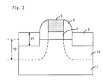
- a thickness of the thermal oxide film may appropriately be adjusted depending on a thickness of the contaminated or damaged surface silicon layer, a junction depth of the source/drain region and the like. Where the silicon layer serves as the source/drain region, it is preferred that the thickness of the thermal oxide film satisfies Y1 ⁇ Y2/X (wherein Y1 is a thickness of the thermal oxide film, Y2 is a junction depth of the source/drain region and X is a ratio of a consumed thickness of silicon layer with respect to the thickness of the thermal oxide film).
- the thickness of the thermal oxide film may be about 5 nm or more.
- a maximum thickness of the thermal oxide film is performed regarding a sheet resistance of 3 ⁇ / ⁇ (flat conversion) as a target value.
- an initial thickness of the silicon layer in the salicide technique is 70 nm.
- the thickness of the silicon oxide film needs to be 55 nm or less (on the assumption that a Si consumption amount X is 0.455 with respect to the silicon oxide film as 1). With the thickness of the silicon oxide film of 55 nm or less, above region of the PN junction becomes the silicide film, the PN junction does not disappear.
- the thermal oxide film is removed.
- the removal of the thermal oxide film may be carried out by a known method such as wet etching using an acidic or alkaline solution, dry etching, sputtering or the like. Among them, wet etching using hydrofluoric acid solution is preferable.
- a silicide film is formed on the resulting silicon layer.
- the silicide film may be formed by a known method of forming a metal film of Ti, Ta, Co, W, Ni, Cr, V, Mo, Nb, Pd or Hf, subjecting the metal film to a thermal treatment, and removing an unreacted part of the metal film.
- a thickness of the metal film may be, for example, about 5 to 70 nm.
- the thermal treatment may be carried out at about 300 to 800 °C.
- the unreacted part of the metal film may be removed by wet etching.
- a layer of TiS 2 , TaSi 2 , WSi 2 , CoSi 2 , NiSi 2 or a layer of a mixture of them may be formed directly on the silicon layer by CVD or sputtering.
- the thickness thereof is preferably smaller than a junction depth of the source/drain region.
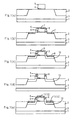
- a device isolation regions 2 are formed on the surface of a semiconductor substrate 1. Boron ions are implanted in a surface region of the semiconductor substrate 1 and activated by a thermal treatment to form a P well 3. Then, a gate insulating film 4 is formed by thermal oxidation and a polysilicon film is deposited on the entire surface by CVD. Then, the polysilicon film is patterned by known lithography and RIE to form a gate electrode 5.
- a silicon oxide film is formed on the entire surface by CVD. Then, the silicon oxide film is anisotropically etched using a reactive ion etching apparatus and ions containing C and F. Accordingly, sidewall films 6 are formed on the sidewalls of the gate electrode 5. At this time, layers 7 contaminated and/or damaged layer by fluorocarbon and/or SiC are formed on the surfaces of the gate electrode 5 and the semiconductor substrate 1.
- boron difluoride ions are implanted in the surface region of the semiconductor substrate 1 and the gate electrode 5.
- the contaminated and/or damaged layers 7 are expanded.
- thermal treatment is carried out using a lamp in a single wafer chamber system under O 2 gas atmosphere at 1100°C for about 22 seconds, thereby a silicon oxide film 9 of about 5 nm thick is deposited.
- the layers 7 that have been existed on the surfaces of the gate electrode 5 and the semiconductor substrate 1 are assimilated into the silicon oxide film 9. Further, heat generated during the formation of the silicon oxide film 9 activates the implanted ions, which forms a source/drain region 10.
- wet etching using a hydrofluoric acid solution or the like is carried out to remove the silicon oxide film 9 existing on the top surface of the gate electrode which is not covered with the sidewall films 26, as well as the layers 7 on the source/drain region 10. At the same time, the silicon surfaces of the gate electrode 5 and the source/drain region 10 are exposed.
- a Ti film of about 35 to 55 nm thick is deposited by sputtering to serve as a refractory metal film.
- the deposition of Ti is carried out under DC of 2000W and Ar of 100 sccm.
- RTA rapid thermal anneal
- N 2 atmosphere at 650 to 700°C for 30 seconds to cause a solid phase reaction between Ti as the refractory metal and silicon so that a high resistive silicide is formed (specific resistance of 70 to 100 ⁇ ⁇ cm).
- the Ti film causes silicide reaction only with the exposed silicon surface but does not react with unexposed silicon.
- unreacted Ti is selectively removed by using a mixture solution of sulfuric acid and hydrogen peroxide so that a silicide film 11 formed by salicide technique is left on the surfaces of the gate electrode 5 and the source/drain region 10.
- Fig. 2 shows the effect on reduction of the sheet resistance of the Ti silicide film formed by the method according to Embodiment of the present invention.
- Fig. 2 shows that the sheet resistance of the Ti silicide film is reduced by about 85 % through the removal of the silicon oxide film of about 5 nm thick using a hydrofluoric acid solution. That is, the removal with the hydrofluoric acid solution allows reduction in sheet resistance of the Ti silicide film.
- the thickness of the silicon oxide film in which the contaminated and/or damaged layer is assimilated is adjusted so as not to exceed the junction depth of the source/drain region 10. That is, the silicon oxide film is formed in a suitable thickness such that a silicon interface below the silicide film to be formed in a later step does not contact an the PN junction. Thus, reduction of junction breakdown voltage is prevented.
- the contaminated and/or damaged layers existing on the surfaces of the gate electrode and the source/drain region before the formation of the silicide film are assimilated into the silicon oxide film formed by thermal oxidation, and then the silicon oxide film is removed to get rid of the damaged and/or contaminated layers. Thereby the increase in sheet resistance of the silicide film is avoided.
- ions implanted in the source/drain region are activated simultaneously with the formation of the silicon oxide film, which simplifies the manufacturing process.
- the surfaces of the gate electrode and the source/drain region are exposed simultaneously with the formation of the silicon oxide film, which simplifies the manufacturing process.
Landscapes
- Electrodes Of Semiconductors (AREA)
- Insulated Gate Type Field-Effect Transistor (AREA)
- Internal Circuitry In Semiconductor Integrated Circuit Devices (AREA)
- Formation Of Insulating Films (AREA)
Abstract
Description
Claims (6)
- A method of manufacturing a semiconductor device comprising the steps of:(a) forming a thermal oxide film on a surface of a silicon layer;(b) removing the thermal oxide film; and(c) forming a silicide film on the resulting surface of the silicon layer.
- A method according to claim 1, wherein the silicon layer serves as a source/drain region of a MOS transistor.
- A method according to claim 1, wherein the silicon layer is a layer contaminated and/or damaged by fluorocarbon and/or SiC.
- A method according to claim 2, wherein the thermal oxide film has a thickness which satisfies Y1<Y2/X, wherein Y1 is a thickness of the thermal oxide film, Y2 is a junction depth of the source/drain region and X is a ratio of a consumed thickness of silicon layer with respect to the thickness of the thermal oxide film.
- A method according to claim 4, wherein the thickness of the thermal oxide film is 5 nm or more.
- A method according to claim 2, wherein the thickness of the silicide film is smaller than a junction depth of the source/drain region.
Applications Claiming Priority (2)
| Application Number | Priority Date | Filing Date | Title |
|---|---|---|---|
| JP2000375582 | 2000-12-11 | ||
| JP2000375582A JP2002184716A (en) | 2000-12-11 | 2000-12-11 | Method for manufacturing semiconductor device |
Publications (2)
| Publication Number | Publication Date |
|---|---|
| EP1213750A2 true EP1213750A2 (en) | 2002-06-12 |
| EP1213750A3 EP1213750A3 (en) | 2005-07-06 |
Family
ID=18844578
Family Applications (1)
| Application Number | Title | Priority Date | Filing Date |
|---|---|---|---|
| EP01122015A Withdrawn EP1213750A3 (en) | 2000-12-11 | 2001-09-13 | Semiconductor device and method of manufacturing the same |
Country Status (5)
| Country | Link |
|---|---|
| US (1) | US6583059B2 (en) |
| EP (1) | EP1213750A3 (en) |
| JP (1) | JP2002184716A (en) |
| KR (1) | KR100462667B1 (en) |
| TW (1) | TW523817B (en) |
Families Citing this family (2)
| Publication number | Priority date | Publication date | Assignee | Title |
|---|---|---|---|---|
| JP2005209836A (en) * | 2004-01-22 | 2005-08-04 | Toshiba Corp | Manufacturing method of semiconductor device |
| JP4343798B2 (en) * | 2004-08-26 | 2009-10-14 | 富士通マイクロエレクトロニクス株式会社 | Manufacturing method of semiconductor device |
Family Cites Families (15)
| Publication number | Priority date | Publication date | Assignee | Title |
|---|---|---|---|---|
| US4716131A (en) * | 1983-11-28 | 1987-12-29 | Nec Corporation | Method of manufacturing semiconductor device having polycrystalline silicon layer with metal silicide film |
| WO1986001641A1 (en) * | 1984-08-24 | 1986-03-13 | American Telephone & Telegraph Company | Mos transistors having schottky layer electrode regions and method of their production |
| US4876213A (en) * | 1988-10-31 | 1989-10-24 | Motorola, Inc. | Salicided source/drain structure |
| ATE139058T1 (en) * | 1990-10-23 | 1996-06-15 | Siemens Ag | METHOD FOR PRODUCING A DOPED POLYZIDE LAYER ON A SEMICONDUCTOR SUBSTRATE |
| JPH06132243A (en) | 1992-10-16 | 1994-05-13 | Oki Electric Ind Co Ltd | Manufacture of semiconductor device |
| KR960014720B1 (en) * | 1993-05-13 | 1996-10-19 | 현대전자산업 주식회사 | Method of formation gate electrode with poly silicide type |
| US5783475A (en) * | 1995-11-13 | 1998-07-21 | Motorola, Inc. | Method of forming a spacer |
| JPH10326837A (en) * | 1997-03-25 | 1998-12-08 | Toshiba Corp | Method of manufacturing semiconductor integrated circuit device, semiconductor integrated circuit device, semiconductor device, and method of manufacturing semiconductor device |
| US5895245A (en) * | 1997-06-17 | 1999-04-20 | Vlsi Technology, Inc. | Plasma ash for silicon surface preparation |
| US6013569A (en) * | 1997-07-07 | 2000-01-11 | United Microelectronics Corp. | One step salicide process without bridging |
| US5972762A (en) * | 1998-01-05 | 1999-10-26 | Texas Instruments--Acer Incorporated | Method of forming mosfets with recessed self-aligned silicide gradual S/D junction |
| WO2000030174A1 (en) * | 1998-11-13 | 2000-05-25 | Intel Corporation | A method and device for improved salicide resistance on polysilicon gates |
| US6171919B1 (en) * | 1999-07-27 | 2001-01-09 | Advanced Micro Devices, Inc. | MOS Transistor formation process including post-spacer etch surface treatment for improved silicide formation |
| US6204136B1 (en) * | 1999-08-31 | 2001-03-20 | Advanced Micro Devices, Inc. | Post-spacer etch surface treatment for improved silicide formation |
| US6368949B1 (en) * | 1999-09-24 | 2002-04-09 | Advanced Micro Devices, Inc. | Post-spacer etch surface treatment for improved silicide formation |
-
2000
- 2000-12-11 JP JP2000375582A patent/JP2002184716A/en active Pending
-
2001
- 2001-09-12 TW TW090122649A patent/TW523817B/en active
- 2001-09-13 EP EP01122015A patent/EP1213750A3/en not_active Withdrawn
- 2001-09-24 US US09/960,513 patent/US6583059B2/en not_active Expired - Fee Related
- 2001-10-19 KR KR10-2001-0064686A patent/KR100462667B1/en not_active Expired - Fee Related
Also Published As
| Publication number | Publication date |
|---|---|
| JP2002184716A (en) | 2002-06-28 |
| KR20020046146A (en) | 2002-06-20 |
| EP1213750A3 (en) | 2005-07-06 |
| US20020072233A1 (en) | 2002-06-13 |
| KR100462667B1 (en) | 2004-12-20 |
| TW523817B (en) | 2003-03-11 |
| US6583059B2 (en) | 2003-06-24 |
Similar Documents
| Publication | Publication Date | Title |
|---|---|---|
| EP0727815B1 (en) | Method for manufacturing semiconductor device with salicide portions | |
| US6562718B1 (en) | Process for forming fully silicided gates | |
| US5940699A (en) | Process of fabricating semiconductor device | |
| US6046090A (en) | Process to fabricate ultra-short channel MOSFETS with self-aligned silicide contact | |
| US6069044A (en) | Process to fabricate ultra-short channel nMOSFETS with self-aligned silicide contact | |
| US6627527B1 (en) | Method to reduce metal silicide void formation | |
| US7371646B2 (en) | Manufacture of insulated gate type field effect transistor | |
| JP3646718B2 (en) | Manufacturing method of semiconductor device | |
| US6583059B2 (en) | Semiconductor device and method of manufacturing the same | |
| US6284612B1 (en) | Process to fabricate ultra-short channel MOSFETs with self-aligned silicide contact | |
| JPH0774129A (en) | Semiconductor device and manufacturing method thereof | |
| JPH10335265A (en) | Method for manufacturing semiconductor device | |
| JPH11307722A (en) | Semiconductor device manufacturing method and semiconductor device | |
| JPH1126397A (en) | Method for manufacturing semiconductor device | |
| US20040058500A1 (en) | Method for forming silicide film of a semiconductor device | |
| JP4095760B2 (en) | Manufacturing method of semiconductor device | |
| JPH11195619A (en) | Method for manufacturing semiconductor device | |
| JP3601232B2 (en) | Method for manufacturing semiconductor device | |
| KR20030095953A (en) | Improvement of titanium disilicide resistance in pinched active regions of semiconductor devices | |
| JP2833530B2 (en) | Method for manufacturing semiconductor device | |
| US20060160361A1 (en) | Nickel salicide process and method of fabricating a semiconductor device using the same | |
| JPH07142447A (en) | Method for manufacturing semiconductor device | |
| KR100291276B1 (en) | Silicide forming method of semiconductor devices | |
| JPH11204784A (en) | Method for manufacturing semiconductor device | |
| KR0161877B1 (en) | Semiconductor device manufacturing method |
Legal Events
| Date | Code | Title | Description |
|---|---|---|---|
| PUAI | Public reference made under article 153(3) epc to a published international application that has entered the european phase |
Free format text: ORIGINAL CODE: 0009012 |
|
| AK | Designated contracting states |
Kind code of ref document: A2 Designated state(s): AT BE CH CY DE DK ES FI FR GB GR IE IT LI LU MC NL PT SE TR |
|
| AX | Request for extension of the european patent |
Free format text: AL;LT;LV;MK;RO;SI |
|
| PUAL | Search report despatched |
Free format text: ORIGINAL CODE: 0009013 |
|
| AK | Designated contracting states |
Kind code of ref document: A3 Designated state(s): AT BE CH CY DE DK ES FI FR GB GR IE IT LI LU MC NL PT SE TR |
|
| AX | Request for extension of the european patent |
Extension state: AL LT LV MK RO SI |
|
| 17P | Request for examination filed |
Effective date: 20050926 |
|
| AKX | Designation fees paid |
Designated state(s): DE FR GB NL |
|
| 17Q | First examination report despatched |
Effective date: 20081028 |
|
| STAA | Information on the status of an ep patent application or granted ep patent |
Free format text: STATUS: THE APPLICATION IS DEEMED TO BE WITHDRAWN |
|
| 18D | Application deemed to be withdrawn |
Effective date: 20090310 |