EP1210772B1 - Method and device for integrated testing for an analog-to-digital converter - Google Patents
Method and device for integrated testing for an analog-to-digital converter Download PDFInfo
- Publication number
- EP1210772B1 EP1210772B1 EP00960825A EP00960825A EP1210772B1 EP 1210772 B1 EP1210772 B1 EP 1210772B1 EP 00960825 A EP00960825 A EP 00960825A EP 00960825 A EP00960825 A EP 00960825A EP 1210772 B1 EP1210772 B1 EP 1210772B1
- Authority
- EP
- European Patent Office
- Prior art keywords
- converter
- code
- counter
- linearities
- input
- Prior art date
- Legal status (The legal status is an assumption and is not a legal conclusion. Google has not performed a legal analysis and makes no representation as to the accuracy of the status listed.)
- Expired - Lifetime
Links
Images


Classifications
-
- H—ELECTRICITY
- H03—ELECTRONIC CIRCUITRY
- H03M—CODING; DECODING; CODE CONVERSION IN GENERAL
- H03M1/00—Analogue/digital conversion; Digital/analogue conversion
- H03M1/10—Calibration or testing
- H03M1/1071—Measuring or testing
- H03M1/109—Measuring or testing for dc performance, i.e. static testing
-
- H—ELECTRICITY
- H03—ELECTRONIC CIRCUITRY
- H03M—CODING; DECODING; CODE CONVERSION IN GENERAL
- H03M1/00—Analogue/digital conversion; Digital/analogue conversion
- H03M1/12—Analogue/digital converters
Definitions
- the present invention relates to analog-digital converters and relates more particularly to the integration of a self-test module which measures the functional characteristics of the converter. such as offset, gain. non-linearities and others, using the principle of the histogram test.
- EP 0 336 715 describes the architecture of an analog-digital converter comprising digital logic for accumulating data from density of codes intended to be used to characterize the converter. The data accumulated by this digital logic is then transmitted to a computer to be processed.
- the invention aims to remedy this drawback by redefining the histogram test technique so as to have only a reduced number of information to be stored on the integrated circuit and to evaluate the characteristics of the converter from simple operations.
- the invention also relates to a self-test device for a converter.
- analog-digital for the implementation of the process defined above, comprising means for applying to the signal converter test, and analysis means, characterized in that said analysis means have common resources integrated with the converter and configurable to successively determine functional characteristics of the converter and means for configuring said analysis means in view to adapt them to the characteristics to be determined.
- the device includes a counter a reference code - comparator connected to the output of the analog-digital converter, an operating and storage up / down counter, the output delivers signals relating to the functional characteristics of the converter and a test phase management controller using said counter-comparator and said up-down counter.
- the invention relates to the integrated test of analog-digital converters.
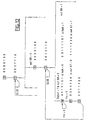
- Figure 1 shows a analog-to-digital converter CAN 1 to the input of which is connected a multiplexer 2 having an input connected to the analog input 3 of the circuit, a input connected to a line 4 for application of a test signal and an input connected to the output of a test stimuli generator 5.
- the CAN 1 is connected to an analysis module 6 which includes an input through which it is connected to line 4 for signal application test and a test output 7, while the CAN has a digital output 8 independent.
- the invention relates more specifically to the analysis module in to promote the possibility of integrating the test technique with CAN histogram.
- the histogram test is based on a statistical analysis of the frequency of appearance of the codes at the output of the converter to be tested.
- each code When a test stimulus is applied to the CAN 1 input, each code must appear a given number of times.
- the principle of the histogram therefore consists in counting the number of times H (i), that each code i actually appears.
- occurrence frequencies H (i) are then used to determine functional characteristics (offset, gain, non-linearities and others) of the converter.
- the basic idea of the invention is to decompose in the time, accumulation and exploitation of the histogram.
- the histogram test considered as an algorithm can be broken down into two dimensions: one temporal, the other spatial.
- the solution according to the invention consists in favoring the temporal breakdown of the algorithm.
- the invention is therefore based on the code-to-code accumulation of the histogram and on a sequential processing of information relating to each coded.
- a second temporal decomposition consists in not determining only one of the functional characteristics at a time.
- Offset k 1 [P (2 not ) - p (1)] k 1 being a known constant.
- k 2 being a known constant
- A being a known constant depending on the number of bits of the converter.
- each code is processed sequentially.
- NLD (i) k 3 p (i)
- the detection of the presence of an output code can be carried out at using a simple comparator and a counter to position the reference code.
- This module which is in fact the module for analyzing the diagram in the figure 1, includes a counter-comparator 10 with n inputs 11 In ⁇ 7: 0> connected to the corresponding CAN outputs (not shown) and representing the 8-bit output from it.
- It also includes an erase or reset input 12, a clock input 13, a control input 14 and an establishment input 15.
- the controller 20 also has an input 23 connected to the outputs CAN, an erase output 24 connected to input 12 of the counter-comparator 10, a code output following 25 connected to the clock input 13, a control output 26 connected to the control input 14 of circuit 10 and a establishment output 27 connected to establishment input 15 of the counter-comparator 10.
- the controller also has a clock input ck28, an input clear 29, a start entry 30, and an end entry 31.
- It also has an output C1 32 and an output C2 33, connected respectively at inputs C1, C2, 34.35 of an up-down counter 36 and an erase output 37 connected to an erase input 38 of the up-down counter 36.
- controller 20 has a multiple input 40 by which it is connected to corresponding outputs 41 of the up-down counter 36.
- the latter has a clock input 42 and a multiple output 43 S ⁇ 6: 0> which is the output of the flip-flops on 8 bits plus a carry-over output and represents the reference code.
- the counter-comparator 10 is shown in detail in FIG. 3.
- each of the eight floors has a set of doors 45a to 45h to which is associated a rocker 46a at 46h.
- the counter or comparator functions of this circuit are determined by the signal from the control circuit 20 and applied to control input 14 + report.
- the comparison function is provided by an EXCLUSIVE NOR gate 47a, one input of which is connected to the input 11 for receiving the signals of analog-to-digital converter output via multiplexer 48a, another input of which is connected via a NAND gate 49a at terminal Q of rocker 46b of the next stage.
- each of the NON-OR EXCLUSIVE doors 47a to 47h is connected to a corresponding input of a NAND gate 50.
- the output of this door constitutes the output 21 of the counter-comparator which delivers the signal Ini-A intended for the controller 20, and which gives the result of the comparison between the reference code and the exit code of the CAN.
- the up-down counter 36 of the circuit of FIG. 2 is represented by detail in figure 4.
- It comprises six groups of doors 52a to 52f with which are associated corresponding flip-flops 53a to 53g.
- Each group of doors such as group 52a has three doors NAND AND 54a, 55a, 56a.
- Gate 54a has two inputs connected respectively to inputs 34.35 of signals C 2 and C 1 .
- the gate 55a is a gate with three inputs, one of which is connected to the input 35 of the signal C 2 , of which a second input is connected via an inverter 57a to an input of an EXCLUSIVE OR gate of the next group of doors 52b, and a third input of which is connected to the output of a NAND door of the group of doors 52b.
- the third door 56a is a door with three inputs of which a first input is connected to the output of the NAND gate of the group of doors 52b, of which a second input is connected to the input 34 of the signal C 1 and of which a third input is connected to the input of the EXCLUSIVE OR gate of the next group of doors 52b.
- the outputs of doors 54a, 55a, 56a are connected to three inputs respective of a NAND gate 58a whose output is connected to an input of a door OR EXCLUSIVE 59a.
- gate 59a is connected to terminal D of flip-flop 53 while that the other input of the EXCLUSIVE OR gate is connected to the Q terminal of the rocker 53a.
- Terminal C of said flip-flop is connected to clock input ck 42, while its RN terminal is connected to the erasing terminal 38.
- the signals Ci and C 2 are also applied to a NOR gate, the output of which is connected via an inverter 61 to an input of an EXCLUSIVE gate 62, the other input of which is connected to the terminal.
- Q of an additional 53g scale.
- the output of gate 62 is connected to terminal D of the flip-flop 53g connected to output 41 of the circuit.
- the terminal Q of the flip-flop 53g is connected to the output 43, while its terminals C and RN are connected respectively to the clock and erase inputs 42 and 38.
- the technique presented makes it possible to determine the characteristics functional such as offset, gain and non-linearity of a converter analog to digital.
- This dynamic test is based on a statistical analysis of the frequency appearance H (i) of each code i at the output of a CAN of n bits.
- the whole test is carried out with a triangular input at the frequency maximum converter operation.
- the offset error is the difference between the actual and theoretical voltages of the input which switches the least significant bit.
- the offset is calculated using two extreme codes which are the only codes changed in the event of an offset error for a triangular signal such as the signal of figure 6.
- the error here has a linear effect on the frequency of appearance of each coded.
- FIG. 7 represents the quantization step as a function of the number N samples for each code.
- the gain error expressed in LSB can be determined using qr.
- A, Te, Tin, PE and q represent respectively the amplitude of the input signal, the sampling period, the signal period input, full scale converter voltage and quantization step ideal.
- the variation of the quantization step for a code i is caused by the non-linearity differential of this code.
- NLI max NLI max ⁇ g
- the accuracy of the gain measurement is very important for the following because it influences all future measures.
- Differential nonlinearities represent the difference from to an LSB, analog values corresponding to two successive codes.
- Integral non-linearities represent the maximum difference between the real characteristic and the ideal transfer line.
- phase 72 the frequency of appearance H (2 n ) of the code 2 n is calculated.
- step 75 the frequency of appearance is calculated H (N1) of the N1 code.
- step 78 it is determined whether N1 ⁇ N2.
- step 79 of initialization of the resources H NLD 0 with a view to passing to phase 3 for calculating non-linearities.
- step 83 all of the resources are again initialized with a view to calculating the frequency of appearance of the code i, then these operations are repeated until calculation during step 84 of the frequency of appearance H (2 n -1) of the code 2 n -1.
- H NLD (2 n -1) H (2 n -1).
- step 85 all of the resources are initialized with a view to computation of integral non-linearities.
- step 86 the frequency of occurrence H (2) is calculated of code 2.
- step 88 the frequency of appearance H (3) of the code 3.
- step 92 all of the resources are initialized with a view to following series of calculations.
- the two blocks 36 and 10 can be grouped in the same block.
- the counter-comparator block 10 allows positioning in the counter the reference code that we want to process and compare it with the converter exit code.
- This block has two functions: place the reference code and compare it with the converter exit code.
- the implementation of the reference code is carried out by incrementing the block output operating in counter mode and comparison in comparator mode is done by reusing the OU-EXCLUSIVE doors 47a at 47h of the counter.
- Control input 12 is required to switch from mode to the other.
- the processing block shown in Figure 4 allows you to perform all the operations required to operate the histogram. As shown in FIG. 4, it is made up of seven flip-flops 53a to 53f and 63 with zero setting and of a combinatorial logic between these different rockers.
- Output 41 is an eight bit output which represents the different characteristics.
- the exit 43 is the exit of the last rocker 53g and forms an entry of the controller.
- the processing block must perform the subtraction between the frequency of appearance of the two extreme codes and must store the result.
- This operation is carried out by configuring the processing block in 7-bit up-down counter.
- the block For the calculation of the other characteristics, the block only has an accumulator function and therefore remains in configuration counter.
- the result contained in the processing block represents the difference between the theoretical value and the actual value of the frequency of appearance H (i) - H tea .
- the two control inputs C1, C2, 34,35 are used to configure the processing block.
- the controller 20 makes it possible to manage all of the test phases.
- the inputs outA5 and outA7 40 represent the carry bits 0 and 1 of the output 41 of the processing block 36.
- the start and end inputs 30,31 are connected to a stimuli generator (not shown) and indicate when the converter output codes are usable.
- the clear or clear input allows initialization of the controller.
- Outputs 32, 33 and 37 deliver control bits C1, C2 and clr-A to processing block 36.
- Output 25 is connected to the clock of the counter-comparator block 10 to issue it a code-following signal.
- the outputs 24, 26, 27 deliver control bits ctr, clr-B and set-B to the counter-comparator 10.
- the stimuli generator provides two binary signals Start and End in addition to the triangular signal.
- the number of periods P of the input signal included in the frame depends on the frequency of the input signal f in , on the sampling frequency f e and on the number of samples to be processed N.
- P ⁇ e * NOT end
- the controller only controls the update input zero and one from the counter.
- the processing block 36 is configured as a down-counter if the code for output is code 00000000 and counter, if the output code is 11111111.
- block 36 performs the subtraction between the frequencies of appearance of the two extreme codes.
- bits C1, C2, cirA, clr-B, set-B, code-sui and ctr have the values 100010 and 1 respectively.
- the controller then waits for the signal (start) from the generator stimuli to start calculating the offset.
- the result is read in the processing block or up-down counter 36 and we take or not the complement of the result according to the carry value 0.
- the gain determination phase will be described with reference to the algorithm calculating the gain shown in Figure 10.
- the gain is calculated using the medium codes. We have to process a number codes important enough to obtain good measurement accuracy.
- the counter is incremented (code 00000101) and the value of the frequency of appearance is added to the previous one.
- the generator For each code, the generator must provide a complete test frame.
- the gain measurement requires 61 frames.
- bits C1, C2, clr-A, clr-B, set-B, code-sui, crt initially have the respective values 0001100.
- the system is on hold: the controller 20 waits for the signal (start) from the stimuli generator to start the gain calculation.
- the counter-comparator 10 counter is then incremented if the reference code is not equal to the last code to be processed (01000000) to determine the gain and we start again without initializing the up-down counter.
- the first code to be processed is positioned at the output of the counter-comparator 10.
- the frequency of appearance of this code is calculated in the up-down counter 36. Then, the up-down counter 36 is initialized and is incremented the counter of the counter-comparator 10 to place the following code and and so on.
- bits C1, C2, clr-A, clr-B, set-B, code-sui, ctr have respectively the following values: 0000100.
- the controller 20 waits for the "start" signal from the stimuli generator (not shown) to start the calculation of non-linearities.
- the integral NLI non-linearities are determined as follows with reference to the calculation algorithm shown in Figure 12.
- the controller 20 waits for the "start" signal from the generator. stimuli to start the calculation of non-linearities.
- the controller 20 waits for the "start" signal from the generator of stimuli to start the computation of integral non-linearities.
- the bits pass to the values: 0011100.
Abstract
Description
La présente invention concerne les convertisseurs analogique-numérique et se rapporte plus particulièrement à l'intégration d'un module d'auto-test qui permet de mesurer les caractéristiques fonctionnelles du convertisseur. telles que le décalage, le gain. les non-linéarités et autres, en utilisant le principe du test par histogramme.The present invention relates to analog-digital converters and relates more particularly to the integration of a self-test module which measures the functional characteristics of the converter. such as offset, gain. non-linearities and others, using the principle of the histogram test.
En ce qui concama le test des convertisseurs analogique-numérique, les industriels utilisent principalement deux méthodes à savoir le test par histogramme et le test par Transformée de Fourier Rapide (TFR).As for the analog-to-digital converter test, manufacturers mainly use two methods, namely the histogram test and the Rapid Fourier Transform (TFR) test.
La mise en oeuvre de ces méthodes nécessite un équipement de test externe performant et très coûteux sous la forme d'un testeur industriel.The implementation of these methods requires test equipment efficient and very expensive external test in the form of an industrial tester.
Une solution classique pour diminuer le coût de ce test externe consiste à intégrer des modules de test à l'intérieur même du circuit.A classic solution to reduce the cost of this external test is to integrate test modules within the circuit itself.
Il est admis que ce type de solution est économiquement viable dans la mesure où la surface des modules ajoutés ne représente que 10 à 15% de la surface originale du circuit.It is recognized that this type of solution is economically viable in since the area of the modules added represents only 10 to 15% of the original surface of the circuit.
L'intégration d'un dispositif de test par histogramme dans sa forme classique pose un problème dans la mesure où la surface des modules de test ajoutée est excessive compte tenu du volume extrêmement important de données à stocker d'une part, et des opérations complexes à réaliser pour permettre l'exploitation d'autre part.Integration of a histogram test device in its form problematic since the surface of the test modules added is excessive given the extremely large volume of data to store on the one hand, and complex operations to perform to allow exploitation on the other hand.
EP 0 336 715 décrit l'architecture d'un convertisseur analogique-numérique
comprenant une logique numérique pour accumuler des données de
densité de codes destinées à être utilisées pour caractériser le convertisseur.
Les données accumulées par cette logique numérique sont ensuite transmises
à un ordinateur pour être traitées.
Le document de J. Raczkowycz et al., "Embedded ADC characterization techniques using a BIST structure, an ADC model and histogram data", Microelectronics Journal, GB, Mackintosh Publications Ltd., Luton, vol. 27, n° 6, 1er septembre 1996, pages 539-549, XP004007233, décrit une technique de test pour caractériser un convertisseur analogique-numérique. Cette technique utilise une mémoire RAM et une cellule d'incrémentation embarquées avec le convertisseur analogique-numérique de manière à réduire le nombre d'informations échangées entre le convertisseur analogique à tester et un appareil de test externe.The document by J. Raczkowycz et al., "Embedded ADC characterization techniques using a BIST structure, an ADC model and histogram data", Microelectronics Journal, GB, Mackintosh Publications Ltd., Luton, vol. 27, No. 6, September 1, 1996, pages 539-549, XP004007233, describes a test technique for characterizing an analog to digital converter. This technique uses a RAM memory and an incrementation cell on board with the analog-digital converter so as to reduce the amount of information exchanged between the analog converter to be tested and an external test device.
Le document de Franck K.Y. MOK et al., "Strech: Self testing reliability evaluation chip", Proceedings of the Custom Integrated Circuits Conférence, US, New York, IEEE vol. Conf. 15, 1993, pages 30.4.1-30.4.4, XP000409779, décrit un circuit ASIC équipé d'une section numérique apte à déterminer une non-linéarité différentielle à partir d'un histogramme de données de codes.The document by Franck K.Y. MOK et al., "Strech: Self testing reliability evaluation chip ", Proceedings of the Custom Integrated Circuits Conférence, US, New York, IEEE vol. Conf. 15, 1993, pages 30.4.1-30.4.4, XP000409779, describes an ASIC circuit equipped with a digital section capable of determining a differential non-linearity from a histogram of code data.
L'invention vise à remédier à cet inconvénient en redéfinissant la technique de test par histogramme de manière à n'avoir qu'un nombre réduit d'informations à stocker sur le circuit intégré et à évaluer les caractéristiques du convertisseur à partir d'opérations simples.The invention aims to remedy this drawback by redefining the histogram test technique so as to have only a reduced number of information to be stored on the integrated circuit and to evaluate the characteristics of the converter from simple operations.
Elle vise également à réaliser un module de test Intégré occupant une faible surface de manière à rendre la solution du test par histogramme économiquement intéressante.It also aims to achieve an Integrated test module occupying a small surface so as to make the histogram test solution economically interesting.
Elle a donc pour objet un procédé de test par histogramme d'un convertisseur analogique-numérique, consistant à décomposer dans le temps, l'accumulation et l'exploitation de l'histogramme, caractàrisé en ce qu'il fait appel à des ressources communes pour traiter successivement les caractéristiques fonctionnelles du convertisseur analogique-numérique et en ce qu'il consiste à initialiser et configurer successivement lesdites ressources en vue de les adapter à la détermination de chacune des caractéristiques fonctionnelles dudit convertisseur.It therefore relates to a histogram test method of a converter analog-digital, consisting in decomposing in time, the accumulation and the exploitation of the histogram, characterized in that it calls upon common resources to deal successively with the functional characteristics of the analog-to-digital converter and what it consists of initializing and successively configure said resources in order to adapt them to the determination of each of the functional characteristics of said converter.
L'invention a également pour objet un dispositif d'auto-test d'un convertisseur analogique-numérique pour la mise en oeuvre du procédé défini ci-dessus, comprenant des moyens d'application au convertisseur de signaux de test, et des moyens d'analyse, caractérisé en ce que lesdits moyens d'analyse comportent des ressources communes intégrées avec le convertisseur et configurables pour déterminer successivement des caractéristiques fonctionnelles du convertisseur et des moyens de configuration desdits moyens d'analyse en vue de les adapter aux caractéristiques à déterminer.The invention also relates to a self-test device for a converter. analog-digital for the implementation of the process defined above, comprising means for applying to the signal converter test, and analysis means, characterized in that said analysis means have common resources integrated with the converter and configurable to successively determine functional characteristics of the converter and means for configuring said analysis means in view to adapt them to the characteristics to be determined.
Selon d'autres caractéristiques, le dispositif comporte un compteur d'un code de référence - comparateur connecté à la sortie du convertisseur analogique-numérique, un compteur/décompteur d'exploitation et de stockage dont la sortie délivre des signaux relatifs aux caractéristiques fonctionnelles du convertisseur et un contrôleur de gestion des phases de test au moyen dudit compteur-comparateur et dudit compteur-décompteur.According to other characteristics, the device includes a counter a reference code - comparator connected to the output of the analog-digital converter, an operating and storage up / down counter, the output delivers signals relating to the functional characteristics of the converter and a test phase management controller using said counter-comparator and said up-down counter.
L'invention sera mieux comprise à la lecture de la description qui va suivre, donnée uniquement à titre d'exemple et faite en se référant aux dessins annexés, sur lesquels :
- la Fig.1 est un schéma synoptique d'un convertisseur analogique-numérique avec un circuit de test incorporé à son circuit intégré;
- la Fig.2 est un schéma synoptique plus détaillé d'un mode de réalisation d'un module d'analyse suivant l'invention;
- la Fig.3 est une représentation plus détaillée du compteur du schéma de la Fig.2;
- la Fig.4 est une représentation plus détaillée du compteur/décompteur du schéma de la Fig.2;
- la Fig.5 est un schéma détaillée d'un organigramme illustrant le calcul du décalage, du gain et des non-linéarités à l'aide du module suivant l'invention;
- la Fig.6 est un graphique montrant la détermination du décalage;
- la Fig.7 est un graphique montrant la détermination du gain;
- la Fig.8 représente un algorithme de test des paramètres essentiels du convertisseur;
- la Fig.9 représente un algorithme de calcul du décalage;
- la Fig.10 représente un algorithme de calcul du gain;
- la Fig.11 représente un algorithme de calcul des non-linéarités différentielles; et
- la Fig.12 représente un algorithme de calcul des non-linéarités intégrales.
- Fig.1 is a block diagram of an analog-digital converter with a test circuit incorporated in its integrated circuit;
- Fig.2 is a more detailed block diagram of an embodiment of an analysis module according to the invention;
- Fig.3 is a more detailed representation of the counter of the diagram in Fig.2;
- Fig.4 is a more detailed representation of the up / down counter of the diagram in Fig.2;
- Fig.5 is a detailed diagram of a flowchart illustrating the calculation of the offset, gain and non-linearities using the module according to the invention;
- Fig.6 is a graph showing the determination of the offset;
- Fig.7 is a graph showing the determination of the gain;
- Fig.8 shows an algorithm for testing the essential parameters of the converter;
- Fig.9 shows an algorithm for calculating the offset;
- Fig.10 shows a gain calculation algorithm;
- Fig.11 shows an algorithm for calculating differential non-linearities; and
- Fig.12 represents an algorithm for calculating integral non-linearities.
L'invention porte sur le test intégré des convertisseurs analogique-numérique.The invention relates to the integrated test of analog-digital converters.
De façon classique, selon une telle solution, il s'agit d'intégrer sur le même silicium que le CAN, un module permettant d'appliquer à l'entrée du convertisseur des stimuli de test et un module permettant d'observer et d'analyser les réponses de sortie du convertisseur.Conventionally, according to such a solution, it involves integrating on the same silicon as CAN, a module allowing to apply to the input of the converter test stimuli and a module to observe and analyze converter output responses.
Un tel agencement est représenté à la figure 1, qui représente un
convertisseur analogique-numérique CAN 1 à l'entrée duquel est connecté un
multiplexeur 2 ayant une entrée connectée à l'entrée analogique 3 du circuit, une
entrée connectée à une ligne 4 d'application d'un signal de test et une entrée
reliée à la sortie d'un générateur 5 de stimuli de test.Such an arrangement is shown in Figure 1, which shows a
analog-to-
A sa sortie, le CAN 1 est connecté à un module d'analyse 6 qui comporte
une entrée par laquelle il est connecté à la ligne 4 d'application des signaux
de test et une sortie de test 7, tandis que le CAN comporte une sortie numérique
8 indépendante.At its output, the CAN 1 is connected to an
Sachant qu'il existe déjà des solutions développées pour la génération de stimuli, l'invention se rapporte plus spécifiquement au module d'analyse en vue de favoriser la possibilité d'intégration au CAN de la technique de test par histogramme.Knowing that there are already solutions developed for the generation of stimuli, the invention relates more specifically to the analysis module in to promote the possibility of integrating the test technique with CAN histogram.
Le test par histogramme est basé sur une analyse statistique de la fréquence d'apparition des codes en sortie du convertisseur à tester.The histogram test is based on a statistical analysis of the frequency of appearance of the codes at the output of the converter to be tested.
En effet, un CAN de n bits possède 2n codes possibles à sa sortie.Indeed, a CAN of n bits has 2 n possible codes at its output.
Lorsqu'un stimulus de test est appliqué à l'entrée du CAN 1, chaque
code doit apparaítre un nombre donné de fois. When a test stimulus is applied to the
Le principe de l'histogramme consiste donc à compter le nombre de fois H(i), que chaque code i apparaít effectivement.The principle of the histogram therefore consists in counting the number of times H (i), that each code i actually appears.
Ces fréquences d'apparition H(i) sont ensuite exploitées pour déterminer les caractéristiques fonctionnelles (décalage, gain, non-linéarités et autres) du convertisseur.These occurrence frequencies H (i) are then used to determine functional characteristics (offset, gain, non-linearities and others) of the converter.
En externe, de manière classique, ce type de test nécessite des ressources matérielles importantes.Externally, conventionally, this type of test requires resources important material.
En effet, pour effectuer le test d'un CAN de n bits, il est nécessaire d'utiliser 2n+1 mots de mémoire pour le stockage de l'histogramme et un processeur de signal numérique DSP ou un microprocesseur pour son exploitation.Indeed, to carry out the test of a CAN of n bits, it is necessary to use 2 n + 1 words of memory for the storage of the histogram and a digital signal processor DSP or a microprocessor for its exploitation.
L'intégration directe de cette technique représente par conséquent, une solution inacceptable puisque la surface occupée par la mémoire et le microprocesseur est largement supérieure à celle du convertisseur lui-même.Direct integration of this technique therefore represents, an unacceptable solution since the surface occupied by the memory and the microprocessor is much greater than that of the converter itself.
De manière à rendre économiquement viable l'intégration du test par histogramme, on redéfinit la technique pour diminuer les ressources nécessaires à son fonctionnement tout en préservant ses performances.In order to make the integration of the test economically viable histogram, we redefine the technique to reduce the resources required to its operation while preserving its performance.
L'idée fondamentale de l'invention consiste à décomposer dans le temps, l'accumulation et l'exploitation de l'histogramme.The basic idea of the invention is to decompose in the time, accumulation and exploitation of the histogram.
En effet, le test par histogramme considéré comme un algorithme, peut être décomposé selon deux dimensions : l'une temporelle, l'autre spatiale.Indeed, the histogram test considered as an algorithm, can be broken down into two dimensions: one temporal, the other spatial.
Sous la contrainte d'une surface minimale imposée pour le module de test intégré au convertisseur, la solution suivant l'invention consiste à privilégier la décomposition temporelle de l'algorithme.Under the constraint of a minimal surface imposed for the module of test integrated into the converter, the solution according to the invention consists in favoring the temporal breakdown of the algorithm.
L'invention est donc basée sur l'accumulation code à code de l'histogramme et sur un traitement séquentiel des informations relatives à chaque code.The invention is therefore based on the code-to-code accumulation of the histogram and on a sequential processing of information relating to each coded.
Pour des contraintes de surface moins strictes, il est possible de calculer et d'exploiter l'histogramme par groupe de codes (2 codes par 2 codes...).For less strict surface constraints, it is possible to calculate and to use the histogram by group of codes (2 codes by 2 codes ...).
A un instant donné du traitement séquentiel, les ressources matérielles requises ne concernent donc que le code en cours.At a given point in the sequential processing, the material resources required therefore only concern the current code.
En effet, après traitement d'un code, ces ressources sont libérées et rendues disponibles pour le code suivant. Indeed, after processing a code, these resources are released and made available for the following code.
De plus, une seconde décomposition temporelle consiste à ne déterminer qu'une seule des caractéristiques fonctionnelles à la fois.In addition, a second temporal decomposition consists in not determining only one of the functional characteristics at a time.
L'analyse est par conséquent décomposée en trois phases.
Lors de l'application de ces trois phases, on a choisi un stimulus d'entrée triangulaire permettant de minimiser les ressources de calcul nécessaires à l'exploitation de l'histogramme.When applying these three phases, an input stimulus was chosen triangular to minimize the computing resources needed to the exploitation of the histogram.
Dans la première phase, seuls les codes extrêmes sont exploités pour
déterminer le décalage.
Dans la deuxième phase, seule une partie des codes du milieu sont
exploités séquentiellement pour déterminer le gain.
![]()
A étant une constante connue dépendant du nombre de bits du convertisseur.In the second phase, only part of the middle codes are used sequentially to determine the gain. ![]()
A being a known constant depending on the number of bits of the converter.
Dans la troisième phase, chaque code est traité séquentiellement. On
obtient ainsi la non-linéarité différentielle NLD(i) associée à chaque code i.
k3 étant une constante connue.k 3 being a known constant.
De plus, le cumul séquentiel de NLD permet d'obtenir la non-linéarité
intégrale NLl(i) associée à chaque code i:

Finalement, le bilan des ressources matérielles nécessaires à l'application de la technique suivant l'invention est le suivant.Finally, the balance of material resources necessary for the application of the technique according to the invention is as follows.
La détection de la présence d'un code en sortie peut être réalisée à l'aide d'un simple comparateur et d'un compteur pour positionner le code de référence. The detection of the presence of an output code can be carried out at using a simple comparator and a counter to position the reference code.
Les différents traitements ne font intervenir que des opérations simples qui peuvent être implantées à l'aide d'un compteur-décompteur.The different treatments only involve simple operations which can be installed using an up-down counter.
La gestion des trois phases de test est assurée par un contrôleur peu complexe.The management of the three test phases is ensured by a little controller complex.
Le schéma de principe d'une implantation possible d'un module de test suivant l'invention est représenté à la figure 2.The schematic diagram of a possible implementation of a module of test according to the invention is shown in Figure 2.
Ce module qui est en fait le module d'analyse du schéma de la figure
1, comporte un compteur-comparateur 10 à n entrées 11 In<7:0> connectées
aux sorties correspondantes du CAN (non représenté) et représentant le code de
sortie à 8 bits de celui-ci.This module which is in fact the module for analyzing the diagram in the figure
1, includes a counter-comparator 10 with
Il comporte en outre une entrée d'effacement ou de mise à zéro 12,
une entrée d'horloge 13, une entrée de contrôle 14 et une entrée d'établissement
15.It also includes an erase or reset
Il comporte de plus des sorties 16 reliées à trois entrées outB2, outB6,
outB8, 17a,17b,17c d'un contrôleur 20 et une sortie 21 reliée à une entrée 22 du
contrôleur 20.It further comprises
Le contrôleur 20 comporte en outre une entrée 23 reliée aux sorties
du CAN, une sortie d'effacement 24 reliée à l'entrée 12 du compteur-comparateur
10, une sortie code suivant 25 connectée à l'entrée d'horloge 13,
une sortie contrôle 26 connectée à l'entrée de contrôle 14 du circuit 10 et une
sortie d'établissement 27 connectée à l'entrée d'établissement 15 du compteur-comparateur
10.The
Le contrôleur comporte en outre une entrée d'horloge ck28, une entrée
d'effacement clear 29, une entrée de début 30, et une entrée de fin 31.The controller also has a clock input ck28, an input
clear 29, a
Il comporte de plus une sortie C1 32 et une sortie C2 33, connectées
respectivement à des entrées C1, C2, 34,35 d'un compteur-décompteur 36 et
une sortie d'effacement 37 connectée à une entrée effacement 38 du compteur-décompteur
36.It also has an
Enfin, le contrôleur 20 comporte une entrée multiple 40 par laquelle il
est connecté à des sorties 41 correspondantes du compteur-décompteur 36.Finally, the
Ce dernier comporte une entrée d'horloge 42 et une sortie multiple 43
S<6:0> qui est la sortie des bascules sur 8 bits plus une sortie de report et représente
le code de référence. The latter has a
Le compteur-comparateur 10 est représenté en détail à la figure 3.The counter-comparator 10 is shown in detail in FIG. 3.
Il est dans le présent exemple réalisé à base d'un compteur à huit bits
dont chacun des huit étages comporte un ensemble de portes 45a à 45h auquel
est associée une bascule 46a à 46h. Les fonctions compteur ou comparateur de
ce circuit sont déterminées par le signal provenant du circuit de contrôle 20 et
appliquées à l'entrée de contrôle 14 + report.In the present example, it is based on an eight-bit counter
each of the eight floors has a set of
La fonction de comparaison est assurée par une porte NON-OU EXCLUSIF
47a dont une entrée est reliée à l'entrée 11 de réception des signaux de
sortie du convertisseur analogique-numérique par l'intermédiaire d'un multiplexeur
48a dont une autre entrée est reliée par l'intermédiaire d'une porte NON-ET
49a à la borne Q de la bascule 46b de l'étage suivant.The comparison function is provided by an EXCLUSIVE NOR
La sortie de chacune des portes NON-OU EXCLUSIF 47a à 47h est
connectée à une entrée correspondante d'une porte NON-ET 50.The exit from each of the
La sortie de cette porte constitue la sortie 21 du compteur-comparateur
qui délivre le signal Ini-A destiné au contrôleur 20, et qui donne le
résultat de la comparaison entre le code de référence et le code de sortie du
CAN.The output of this door constitutes the
Le compteur-décompteur 36 du circuit de la figure 2 est représenté en
détail à la figure 4.The up-
Il comporte six groupes de portes 52a à 52f auxquelles sont associées
des bascules correspondantes 53a à 53g.It comprises six groups of
Chaque groupe de portes tel que le groupe 52a comporte trois portes
NON-ET 54a,55a,56a.Each group of doors such as
La porte 54a a deux entrées connectées respectivement aux entrées 34,35 des signaux C2 et C1.Gate 54a has two inputs connected respectively to inputs 34.35 of signals C 2 and C 1 .
La porte 55a est une porte à trois entrées dont l'une est reliée à l'entrée
35 du signal C2, dont une seconde entrée est connectée par l'intermédiaire
d'un inverseur 57a à une entrée d'une porte OU EXCLUSIF du groupe de portes
52b suivant, et dont une troisième entrée est connectée à la sortie d'une porte
NON-ET du groupe de portes 52b.The gate 55a is a gate with three inputs, one of which is connected to the
La troisième porte 56a est une porte à trois entrées dont une première
entrée est connectée à la sortie de la porte NON-ET du groupe de portes 52b,
dont une seconde entrée est connectée à l'entrée 34 du signal C1 et dont une
troisième entrée est connectée à l'entrée de la porte OU EXCLUSIF du groupe
de portes 52b suivant.The
Les sorties des portes 54a, 55a,56a sont connectées à trois entrées
respectives d'une porte NON-ET 58a dont la sortie est reliée à une entrée d'une
porte OU EXCLUSIF 59a.The outputs of
La sortie de la porte 59a est reliée à la borne D de la bascule 53 tandis que l'autre entrée de la porte OU EXCLUSIF est connectée à la borne Q de la bascule 53a.The output of gate 59a is connected to terminal D of flip-flop 53 while that the other input of the EXCLUSIVE OR gate is connected to the Q terminal of the rocker 53a.
La borne C de ladite bascule est connectée à l'entrée d'horloge ck 42,
tandis que sa borne RN est connectée à la borne d'effacement 38.Terminal C of said flip-flop is connected to clock input
Les autres étages du compteur-décompteur sont identiques et ne seront donc pas décrits.The other stages of the up-down counter are identical and will not be therefore not described.
Les signaux Ci et C2 sont par ailleurs appliqués à une porte NON-OU
dont la sortie est connectée par l'intermédiaire d'un inverseur 61 à une entrée
d'une porte OU EXCLUSIF 62 dont l'autre entrée est reliée à la borne Q d'une
bascule 53g supplémentaire. La sortie de la porte 62 est connectée à la borne D
de la bascule 53g reliée à la sortie 41 du circuit. La borne Q de la bascule 53g
est reliée à la sortie 43, tandis que ses bornes C et RN sont connectées respectivement
aux entrées d'horloge et d'effacement 42 et 38.The signals Ci and C 2 are also applied to a NOR gate, the output of which is connected via an
La technique présentée permet de déterminer les caractéristiques fonctionnelles telles que le décalage, le gain et les non-linéarités d'un convertisseur analogique-numérique.The technique presented makes it possible to determine the characteristics functional such as offset, gain and non-linearity of a converter analog to digital.
Ce test dynamique est basé sur une analyse statistique de la fréquence d'apparition H(i) de chaque code i à la sortie d'un CAN de n bits.This dynamic test is based on a statistical analysis of the frequency appearance H (i) of each code i at the output of a CAN of n bits.
L'ensemble du test s'effectue avec une entrée triangulaire à la fréquence maximale de fonctionnement du convertisseur.The whole test is carried out with a triangular input at the frequency maximum converter operation.
Pour ce type de signal, la fréquence d'apparition théorique Hthé a la même valeur pour tous les codes Hthé = N / 2 n .For this type of signal, the frequency of theoretical appearance H tea has the same value for all the codes H tea = N / 2 n .
Elle dépend uniquement du nombre N d'échantillons et du nombre n de bits du convertisseur.It only depends on the number N of samples and the number n bits of the converter.
On va maintenant décrire en référence aux figures 6 et 7, la détermination du décalage et du gain. We will now describe with reference to FIGS. 6 and 7, the determination offset and gain.
La définition classique de l'erreur de décalage est la suivante. Dans un CAN, l'erreur de décalage est la différence entre les tensions réelle et théorique de l'entrée qui fait commuter le bit de poids le plus faible.The classic definition of the offset error is as follows. In one CAN, the offset error is the difference between the actual and theoretical voltages of the input which switches the least significant bit.
Selon l'invention, le décalage est calculé à l'aide de deux codes extrêmes qui sont les seuls codes modifiés dans le cas d'une erreur de décalage pour un signal triangulaire tel que le signal de la figure 6.According to the invention, the offset is calculated using two extreme codes which are the only codes changed in the event of an offset error for a triangular signal such as the signal of figure 6.
L'erreur a ici un effet linéaire sur la fréquence d'apparition de chaque code.The error here has a linear effect on the frequency of appearance of each coded.
Par conséquent, on arrive à une expression très simple du décalage
exprimé en LSB :
Si par exemple, on désire mesurer une erreur supérieure à 1 LSB, il
faut augmenter l'amplitude du signal d'entrée. En effet, si l'amplitude du signal
d'entrée correspond juste à la pleine échelle PE du convertisseur et si le décalage
est supérieur à 1 LSB, le code 00....00 ne sera jamais présent à la sortie du
convertisseur.If, for example, we want to measure an error greater than 1 LSB, it
increase the amplitude of the input signal. Indeed, if the signal amplitude
input just corresponds to the full scale PE of the converter and if the offset
is greater than 1 LSB, the
La valeur minimale de l'amplitude d'entrée dépend directement du décalage
maximum mesuré.
On va maintenant décrire la détermination du gain en référence à la figure 7, qui représenté le pas de quantification en fonction du nombre N d'échantillons pour chaque code. We will now describe the determination of the gain with reference to the FIG. 7, which represents the quantization step as a function of the number N samples for each code.
Si le convertisseur a un gain g différent de 1, son pas de quantification qr est toujours constant, mais il a une valeur g fois plus petite que dans le cas idéal qr=q/g.If the converter has a gain g other than 1, its quantization step qr is always constant, but it has a value g times smaller than in the case ideal qr = q / g.
Par une étude similaire à celle du décalage, qr peut être obtenu assez
facilement :
L'erreur de gain exprimée en LSB peut être déterminée grâce à qr.
Dans cette équation, A, Te, Tin, PE et q représentent respectivement l'amplitude du signal d'entrée, la période d'échantillonnage, la période du signal d'entrée, la tension pleine échelle du convertisseur et le pas de quantification idéal.In this equation, A, Te, Tin, PE and q represent respectively the amplitude of the input signal, the sampling period, the signal period input, full scale converter voltage and quantization step ideal.
Cette mesure ne peut être réalisée sur un seul code, car il faut prendre en compte les variations du pas de quantification dues aux non-linéarités du convertisseur.This measurement cannot be carried out on a single code, because it is necessary to take account for the variations in the quantization step due to the non-linearities of the converter.
La moindre erreur de non-linéarité sur le code pris comme référence va être répercutée sur la mesure du gain.The slightest non-linearity error on the code taken as reference will be passed on to the gain measurement.
Par conséquent, la mesure va porter sur plusieurs codes différents. La variation du pas de quantification pour un code i est causée par la non-linéarité différentielle de ce code.Consequently, the measurement will relate to several different codes. The variation of the quantization step for a code i is caused by the non-linearity differential of this code.
Par contre, pour une variation due à plusieurs codes, il est intéressant d'étudier l'influence de l'incertitude sur la non-linéarité intégrale.On the other hand, for a variation due to several codes, it is interesting to study the influence of uncertainty on integral non-linearity.
On se place dans le cas extrême où la variation du pas de quantification due aux non-linéarités des codes étudiés est égale à la non-linéarité intégrale maximale admise.We place ourselves in the extreme case where the variation of the quantization step due to the non-linearities of the codes studied is equal to the integral non-linearity maximum allowed.
Pour une précision de mesure sur le gain de Δg et une erreur de non-linéarité
intégrale maximum, NLImax, le nombre de codes est égal au rapport
NLImax par Δg.
La précision de la mesure du gain est très importante pour la suite parce qu'elle influence toutes les mesures futures.The accuracy of the gain measurement is very important for the following because it influences all future measures.
Par exemple, avec des contraintes assez strictes :For example, with fairly strict constraints:
NLImax = 1. LSB et une bonne précision de mesure, soit Δg = 0,02 LSB.NLI max = 1. LSB and good measurement accuracy, ie Δg = 0.02 LSB.
Il est nécessaire de calculer la moyenne de l'erreur de gain sur 50 codes.It is necessary to calculate the mean of the gain error over 50 codes.
On va maintenant décrire la détermination des non-linéarités.We will now describe the determination of non-linearities.
On peut définir deux types de non-linéarités:
- les non-linéarités différentielles (NLD)
- les non-linéarités intégrales.
- differential non-linearities (NLD)
- integral nonlinearities.
Les non-linéarités différentielles représentent la différence par rapport à un LSB, des valeurs analogiques correspondantes à deux codes successifs.Differential nonlinearities represent the difference from to an LSB, analog values corresponding to two successive codes.
Dans la présente technique, elles sont déterminées directement à partir
de la fréquence d'apparition du code auquel elles se rapportent.
Les non-linéarités intégrales (NLI) représentent l'écart maximal entre la caractéristique réelle et la droite de transfert idéale.Integral non-linearities (NLI) represent the maximum difference between the real characteristic and the ideal transfer line.
Elles sont calculées en accumulant les NLD.
![]()
![]()
On va maintenant décrire en référence à la figure 5, l'algorithme global de la technique suivant l'invention.We will now describe with reference to FIG. 5, the global algorithm of the technique according to the invention.
On notera que toutes les ressources du système sont réutilisables après chaque initialisation. De ce fait, les ressources globales nécessaires à l'application de la technique de l'invention sont faibles et donc la structure est facilement intégrable à un convertisseur analogique-numérique.Note that all the resources of the system are reusable after each initialization. As a result, the overall resources required to the application of the technique of the invention are weak and therefore the structure is easily integrated into an analog-digital converter.
L'algorithme est représenté à la figure 5 sous la forme d'un organigramme.The algorithm is shown in Figure 5 in the form of a flowchart.
Il comporte :
une phase 1 de calcul du décalage,une phase 2 de calcul du gain,une phase 3 de calcul des non-linéarités différentielles et intégrales.
- a
phase 1 for calculating the offset, - a
phase 2 of gain calculation, - a
phase 3 of calculating the differential and integral non-linearities.
La phase 1 comprend une étape 70 d'initialisation de toutes les ressources
Hdec = 0.
Puis, au cours d'une étape 71, on calcule la fréquence d'apparition
H(o) du code 0.Then, during a step 71, the frequency of appearance is calculated
H (o) of
Au cours de la phase 72, on calcule la fréquence d'apparition H(2n) du
code 2n.During
Au cours de l'étape 73, on procède au calcul de Hdec = H(2n)-H(0).During
Ces opérations sont réalisées avec les ressources décrites en référence aux figures 2 à 4 programmées pour assurer le calcul du décalage.These operations are carried out with the resources described in reference Figures 2 to 4 programmed to calculate the offset.
Au cours de l'étape 74, on procède à l'initialisation des ressources en
vue de la phase 2 de calcul du gain. A l'issue de cette initialisation Hgain= 0.During step 74, the resources are initialized with a view to
Puis, au cours de l'étape 75, on calcule la fréquence d'apparition H(N1) du code N1.Then, during step 75, the frequency of appearance is calculated H (N1) of the N1 code.
Au cours de l'étape 76, on accumule avec la valeur de gain précédente, Hgain=Hgain + H(N1).During step 76, we accumulate with the previous gain value, H gain = H gain + H (N1).
Au cours de l"étape 77, on procède à l'incrémentation du code de référence
N1 : N1=N1+1.During
Au cours de l'étape 78, on détermine si N1 < N2.During
Dans l'affirmative, on retourne à l'étape 75 de calcul de la fréquence d'apparition H(N1) du code N1.If so, we return to step 75 of calculating the frequency of appearance H (N1) of the code N1.
Dans la négative, on passe à l'étape 79 d'initialisation des ressources
HNLD= 0 en vue du passage à la phase 3 de calcul des non-linéarités.If not, we go to step 79 of initialization of the resources H NLD = 0 with a view to passing to
Lors de l'étape 80, on calcule la fréquence d'apparition H(2) du code
2, HNLD(2) = H(2).During
Au cours de l'étape 81, on initialise à nouveau toutes les ressources
HNLD = 0.During
Au cours de l'étape 82, on calcule la fréquence d'apparition H(3) du
code 3, HNLD(3) = H(3),During
Au cours de l'étape 83, on initialise à nouveau l'ensemble des ressources
en vue du calcul de la fréquence d'apparition du code i, puis on recommence
ces opérations jusqu'au calcul au cours de l'étape 84 de la fréquence
d'apparition H(2n-1) du code 2n-1. HNLD(2n-1) = H(2n-1).During step 83, all of the resources are again initialized with a view to calculating the frequency of appearance of the code i, then these operations are repeated until calculation during
Au cours de l'étape 85, on initialise toutes les ressources en vue du calcul des non-linéarités intégrales.During step 85, all of the resources are initialized with a view to computation of integral non-linearities.
Puis au cours de l'étape 86, on calcule la fréquence d'apparition H(2)
du code 2.Then during
Au cours de l'étape 87, on procède à l'accumulation avec la valeur précédente HNLI = HNLI + H(2).During step 87, the accumulation is carried out with the previous value H NLI = H NLI + H (2).
Au cours de l'étape 88, on calcule la fréquence d'apparition H(3) du
code 3.During
Au cours de l'étape 89, on procède à l'accumulation avec la valeur
précédente HNLI = HNLI + H(3) et ainsi de suite jusqu'au calcul du cours de l'étape
90 de la fréquence d'apparition H(2n-1) du code 2n-1.During
Au cours de l'étape 91, on procède à l'accumulation avec la valeur
précédente et on aboutit à l'obtention de la non-linéarité intégrale HNLI = HNLI +(2n-1).During the
Enfin, à l'étape 92, on initialise l'ensemble des ressources en vue de la
série de calculs suivante.Finally, in
On donne ci-après un exemple pratique de réalisation d'un convertisseur analogique-numérique à module d'auto-test implanté.
- convertisseur analogique-
numérique 8 bits (256 codes), - fréquence d'échantillonnage 10 Mhz
- fréquence du
signal d'entrée - 8192 échantillons par trame de test. Donc 1000 périodes du signal d'entrée pour chaque trame,
- erreur de décalage admise ± 1,5 LSB
- erreur de gain admise ± 1,5 LSB,
- non-linéarités différentielles admises ± 0,5 LSB,
- non-linéarités intégrales admises ± 0,5 LSB.
- 8-bit analog-to-digital converter (256 codes),
- sampling
frequency 10 Mhz - frequency of the
input signal - 8192 samples per test frame. So 1000 periods of the input signal for each frame,
- allowed offset error ± 1.5 LSB
- gain error allowed ± 1.5 LSB,
- allowed differential non-linearities ± 0.5 LSB,
- permissible integral non-linearities ± 0.5 LSB.
Les ressources matérielles nécessaires à la mise en oeuvre de l'invention sont représentées à la figure 2.The material resources necessary for the implementation of the invention are shown in Figure 2.
Elles comportent
- un bloc de détection de la présence d'un code à la sortie du convertisseur analogique-numérique.
- a block for detecting the presence of a code at the output of the analog-digital converter.
Ce bloc représenté en 10 à la figure 2, est comme indiqué plus haut, un compteur comparateur pour positionner le code de référence.
un bloc 36 d'exploitation d'histogramme, il est réalisé sous la forme d'un compteur-décompteur à complément à 1,un bloc 20 de gestion des trois phases de test ou contrôleur.
- a
block 36 for histogram processing, it is produced in the form of a counter-down counter with 1 complement, - a
block 20 for managing the three test phases or controller.
Les deux blocs 36 et 10 peuvent être regroupés dans un même bloc.The two
L'implantation de cette technique est décrite en référence aux figures 3 et 4. Elle est avantageusement réalisée en technologie AMSO,8µm.The implementation of this technique is described with reference to the figures 3 and 4. It is advantageously carried out in AMSO technology, 8 μm.
On va maintenant détailler la construction et le fonctionnement de chaque bloc.We will now detail the construction and operation of each block.
Le bloc compteur-comparateur 10 permet de positionner dans le
compteur le code de référence que l'on désire traiter et de le comparer avec le
code de sortie du convertisseur.The
Il est constitué de 8 bascules 46a à 46h avec mise à un et mise à zéro
reliées par de la logique combinatoire décrite en référence à la figure 3.It consists of 8
Ce bloc a deux fonctions : placer le code de référence et le comparer avec le code de sortie du convertisseur.This block has two functions: place the reference code and compare it with the converter exit code.
La mise en place du code de référence est réalisée en incrémentant la
sortie du bloc fonctionnant en mode compteur et la comparaison en mode comparateur
s'effectue en réutilisant les portes OU-EXCLUSIF 47a à 47h du compteur.The implementation of the reference code is carried out by incrementing the
block output operating in counter mode and comparison in comparator mode
is done by reusing the OU-
L'entrée de commande 12 est nécessaire pour passer d'un mode à
l'autre.
Si l'entrée de commande 12 reçoit un signal crt = 0, le bloc est placé
en mode compteur et la sortie est incrémentée à chaque front d'horloge.If the
Si l'entrée de commande 12 reçoit un signal ctr = 1, le bloc effectue la
comparaison entre le code de référence, out<7:0> et le code de sortie du convertisseur
I1<7:0>.If the
Si les deux codes sont égaux, Ini-A passe à zéro.If the two codes are equal, Ini-A goes to zero.
Si les deux codes sont différents, Ini-A passe à un. If the two codes are different, Ini-A goes to one.
Le bloc de traitement représenté à la figure 4 permet d'effectuer toutes les opérations nécessaires à l'exploitation de l'histogramme. Comme représenté à la figure 4, il est constitué de sept bascules 53a à 53f et 63 avec mise à zéro et d'une logique combinatoire entre ces différentes bascules.The processing block shown in Figure 4 allows you to perform all the operations required to operate the histogram. As shown in FIG. 4, it is made up of seven flip-flops 53a to 53f and 63 with zero setting and of a combinatorial logic between these different rockers.
La sortie 41 est une sortie de huit bits qui représente les différentes
caractéristiques.
La sortie 43 est la sortie de la dernière bascule 53g et forme une entrée
du contrôleur.The
Pour calculer le décalage, le bloc de traitement doit effectuer la soustraction entre la fréquence d'apparition des deux codes extrêmes et doit stocker le résultat.To calculate the offset, the processing block must perform the subtraction between the frequency of appearance of the two extreme codes and must store the result.
Cette opération est réalisée en configurant le bloc de traitement en compteur-décompteur à 7 bits. Pour le calcul des autres caractéristiques, le bloc de traitement n'a qu'une fonction d'accumulateur et reste donc en configuration de compteur.This operation is carried out by configuring the processing block in 7-bit up-down counter. For the calculation of the other characteristics, the block only has an accumulator function and therefore remains in configuration counter.
Le résultat contenu dans le bloc de traitement représente la différence entre la valeur théorique et la valeur réelle de la fréquence d'apparition H(i) - Hthé.The result contained in the processing block represents the difference between the theoretical value and the actual value of the frequency of appearance H (i) - H tea .
Pour pouvoir exploiter le résultat, il faut tenir compte du signe de cette différence.To be able to use the result, you must take into account the sign of this difference.
Si la valeur stockée dans le bloc 36 est négative, la sortie est complémentée
à 1.If the value stored in
Les deux entrées de contrôle C1, C2, 34,35, sont utilisées pour configurer le bloc de traitement.The two control inputs C1, C2, 34,35, are used to configure the processing block.
Il y a quatre modes de fonctionnement :
Le contrôleur 20 permet de gérer l'ensemble des phases de test.The
Les entrées reçoivent les signaux suivants :
- Ini-
A 22 donne le résultat de la comparaison entre le code de sortie du CAN et le code de référence. InO 23 reçoit le bit de poids faible du code de sortie du convertisseur.L'entrée 28 est l'entrée du signal d'horloge ck du contrôleur.Les entrées bits comparateur 10.
- Ini-
A 22 gives the result of the comparison between the CAN output code and the reference code. -
InO 23 receives the least significant bit of the converter output code. - The
input 28 is the input of the clock signal ck of the controller. - The
inputs bits counter-comparator block 10 respectively.
Les entrées outA5 et outA7 40 représentent les bits de report 0 et 1 de
la sortie 41 du bloc de traitement 36.The inputs outA5 and
Les entrées 30,31 de début et fin sont reliées à un générateur de stimuli
(non représenté) et indiquent quand les codes de sortie du convertisseur
sont exploitables. L'entrée d'effacement ou clear permet l'initialisation du contrôleur.The start and end
Les sorties 32,33 et 37 délivrent des bits de contrôle C1, C2 et clr-A
vers le bloc de traitement 36.
La sortie 25 est connectée à l'horloge du bloc compteur-comparateur
10 pour lui délivrer un signal code-suivant.
Les sorties 24,26,27 délivrent des bits de contrôle ctr, clr-B et set-B au
compteur-comparateur 10.The
Le fonctionnement général du comparateur est détaillé dans l'algorithme représenté à la figure 8.The general operation of the comparator is detailed in the algorithm shown in figure 8.
Durant toutes les phases de test décrites ci-dessous, on considère que le générateur de stimuli fournit deux signaux binaires Début et Fin en plus du signal triangulaire.During all the test phases described below, we consider that the stimuli generator provides two binary signals Start and End in addition to the triangular signal.
Ces signaux désignent le début et la fin de chaque trame de test.These signals designate the start and end of each test frame.
Le nombre de périodes P du signal d'entrée comprises dans la trame
dépend de la fréquence du signal d'entrée fin, de la fréquence d'échantillonnage
fe et du nombre d'échantillon à traiter N.
Il est nécessaire de gérer autant de trames que de codes à traiter durant les différentes phases.It is necessary to manage as many frames as there are codes to process during the different phases.
Dans cette phase dont l'algorithme de calcul est représenté à la figure
9, le compteur du compteur-comparateur 10 ne doit avoir en sortie que deux valeurs
00.....00 ou 11.....11.In this phase, the calculation algorithm of which is shown in Figure
9, the counter of the counter-comparator 10 must only have two values at the
Par conséquent, le contrôleur ne commande que l'entrée de mise à zéro et à un du compteur.Therefore, the controller only controls the update input zero and one from the counter.
Le bloc de traitement 36 est configuré en décompteur si le code de
sortie est le code 00000000 et en compteur, si le code de sortie est 11111111.The
De ce fait, le bloc 36 effectue la soustraction entre les fréquences d'apparition des deux codes extrêmes.Therefore, block 36 performs the subtraction between the frequencies of appearance of the two extreme codes.
Cette différence est proportionnelle au décalage comme on peut le voir d'après l'équation (1).This difference is proportional to the shift as can be see from equation (1).
Durant cette phase, le traitement des deux codes extrêmes s'effectue simultanément et ne nécessite donc qu'une trame de test.During this phase, the two extreme codes are processed simultaneously and therefore only requires one test frame.
On voit sur l'algorithme de calcul de la figure 9 que les bits C1, C2, cirA,
clr-B, set-B, code-sui et ctr, ont respectivement les valeurs 100010 et 1.We see on the calculation algorithm of FIG. 9 that the bits C1, C2, cirA,
clr-B, set-B, code-sui and ctr, have the
L'initialisation de l'ensemble des blocs est assurée par :
- la mise à zéro du bloc de traitement 36(clr-A=0)
- mise à zéro du compteur-comparateur 10 B(clr-B = 0).
- zeroing of processing block 36 (clr-A = 0)
- zeroing of the counter-comparator 10 B (clr-B = 0).
Les bits précités passent alors aux états suivants :
Le contrôleur attend alors le signal (début) provenant du générateur de stimuli pour commencer le calcul du décalage.The controller then waits for the signal (start) from the generator stimuli to start calculating the offset.
Le signal début passe à 1 et le calcul du décalage a lieu. Il se poursuit tant que le signal Fin=0.The start signal goes to 1 and the offset calculation takes place. It continues as long as the signal End = 0.
Ce calcul est assuré par le positionnement du compteur du compteur-comparateur 10 au code O ou 1 (clr-B/set-B) suivant que In0 est égal à O ou 1. This calculation is ensured by the positioning of the counter of the counter-comparator 10 to code O or 1 (clr-B / set-B) depending on whether In0 is equal to O or 1.
Ensuite, il y a comparaison entre ie sortie du compteur et le code de sortie du CAN (In).Then, there is comparison between the output of the counter and the code of CAN (In) output.
Ensuite, il y a incrémentation ou décrémentation du compteur 36 suivant
le résultat et la valeur de In0 et le résultat de la comparaison (valeur de Ini-A)Then, there is incrementation or decrementation of the following
A la fin du calcul du décalage, les bits précités ont les valeurs suivantes
:
Le résultat est lu dans le bloc de traitement ou compteur-décompteur
36 et l'on prend ou non le complément du résultat suivant la valeur de report 0.The result is read in the processing block or up-
Les bits précités sont alors les valeurs respectives suivantes :
La phase de détermination du gain va être décrite en référence à l'algorithme de calcul du gain représenté à la figure 10.The gain determination phase will be described with reference to the algorithm calculating the gain shown in Figure 10.
Le gain est calculé à l'aide des codes milieux. II faut traiter un nombre de codes assez important pour obtenir une bonne précision de mesure.The gain is calculated using the medium codes. We have to process a number codes important enough to obtain good measurement accuracy.
A cet effet, on cumule par exemple la fréquence d'apparition de 61 codes répartis entre le troisième et le soixante quatrième.For this purpose, we cumulate for example the frequency of appearance of 61 codes distributed between the third and the sixty-fourth.
On commencera par placer la premier code de référence dans le compteur du compteur-comparateur 10 (code 00000100).We will start by placing the first reference code in the counter of the comparator 10 (code 00000100).
On calcule la fréquence d'apparition de ce code. The frequency of appearance of this code is calculated.
Ensuite, le compteur est incrémenté (code 00000101) et la valeur de la fréquence d'apparition est ajoutée à la précédente.Then, the counter is incremented (code 00000101) and the value of the frequency of appearance is added to the previous one.
Cette opération est répétée jusqu'au dernier code à traiter (code
01000000). Le résultat peut alors être extrait du bloc de traitement 36.This operation is repeated until the last code to be processed (code
01000000). The result can then be extracted from the
Pour chaque code, le générateur doit fournir une trame de test complète.For each code, the generator must provide a complete test frame.
Pour l'exemple traité ici, la mesure du gain nécessite 61 trames.For the example treated here, the gain measurement requires 61 frames.
Les opérations sont les suivantes.The operations are as follows.
Lors de l'initialisation, les bits C1,C2,clr-A, clr-B, set-B, code-sui, crt, ont initialement les valeurs respectives 0001100.During initialization, bits C1, C2, clr-A, clr-B, set-B, code-sui, crt, initially have the respective values 0001100.
On initialise alors le compteur-décompteur 36 et le compteur-comparateur
10.We then initialize the up-
Puis les bits précités passent aux valeurs respectives suivantes :
Il y a mise en place du code de référence sur le compteur du compteur-comparateur 10, puis incrémentation de ce compteur jusqu'au code 00000100 = premier code traité pour déterminer le gain, incrémentation tant que outB2=0.There is implementation of the reference code on the counter of the counter-comparator 10, then increment this counter up to the code 00000100 = first code processed to determine the gain, increment as long as outB2 = 0.
Lorsque outB2=1, les bits précités prennent les valeurs 0011110.When outB2 = 1, the above bits take the values 0011110.
Le système est en attente : le contrôleur 20 attend le signal (début)
provenant du générateur de stimuli pour commencer le calcul du gain.The system is on hold: the
Le signal début passe à Début = 1.The start signal changes to Start = 1.
Les bits précités passent alors aux valeurs suivantes :
Il y a calcul du gain tant que le signal Fin=0. The gain is calculated as long as the signal End = 0.
Il y a comparaison entre ia sortie du compteur du compteur-comparateur 10 et le code de sortie du CAN (In).There is a comparison between the output of the counter of the counter-comparator 10 and the CAN exit code (In).
Suivant le résultat de cette comparaison, il y a incrémentation du
compteur-décompteur 36.Depending on the result of this comparison, there is an increment of the
up-
Les bits précités passent alors aux valeurs suivantes 0011100.The above bits then pass to the following
On incrémente alors de compteur du compteur-comparateur 10 si le code de référence n'est pas égal au dernier code à traiter (01000000) pour déterminer le gain et on recommence sans initialiser le compteur-décompteur.The counter-comparator 10 counter is then incremented if the reference code is not equal to the last code to be processed (01000000) to determine the gain and we start again without initializing the up-down counter.
Lorsque le signal outB6=1, les bits précités passent aux valeurs suivantes
:
On lit le résultat dans le bloc de traitement 36 et on prend ou non le
complément du résultat suivant la valeur de outA5.We read the result in
On va maintenant décrire la phase de détermination des non-linéarités.We will now describe the phase of determining the non-linearities.
On commence par les non-linéarités différentielles. La phase de détermination des non-linéarités différentielles va être décrite en référence à l'algorithme de calcul des NLD représenté figure 11.We start with the differential non-linearities. The determination phase differential non-linearities will be described with reference to the algorithm NLD calculation shown in figure 11.
Le premier code à traiter est positionné à la sortie du compteur-comparateur 10.The first code to be processed is positioned at the output of the counter-comparator 10.
La fréquence d'apparition de ce code est calculée dans le compteur-décompteur
36. Ensuite, le compteur-décompteur 36 est initialisé et on incrémente
le compteur du compteur-comparateur 10 pour placer le code suivant et
ainsi de suite.The frequency of appearance of this code is calculated in the up-
Une trame complète (Ppériodes) du signal d'entrée est nécessaire pour chaque code (traitement séquentiel).A complete frame (Periods) of the input signal is required for each code (sequential processing).
Lors de l'initialisation, les bits C1,C2,clr-A, clr-B, set-B, code-sui, ctr, ont respectivement les valeurs suivantes : 0000100. During initialization, bits C1, C2, clr-A, clr-B, set-B, code-sui, ctr, have respectively the following values: 0000100.
Il y a initialisation des circuits 36 et 10.There is initialization of
Puis, les bits précités passent aux valeurs suivantes 0011110. Le
contrôleur 20 attend le signal "début" provenant du générateur de stimuli (non
représenté) pour commencer le calcul des non-linéarités.Then, the aforementioned bits pass to the following values 0011110. The
Lorsque les signaux début=1 et outB8=0, les bits précités prennent les
valeurs suivantes :
Tant que Fin=0, il y a calcul des non-linéarités. Il y a comparaison entre
la sortie du circuit 10 et le code de sortie du CAN(In), puis incrémentation ou
non du circuit 36 suivant le résultat.As long as End = 0, there is calculation of non-linearities. There is comparison between
the output of
Lorsque Fin=1, les bits précités passent ensuite aux valeurs suivantes:
Puis, il y a lecture du résultat dans le circuit 36 et complémentation ou
pas de ce résultat suivant la valeur de outA5.Then, there is reading of the result in
Enfin, les bits précités prennent les valeurs suivantes 0001100.Finally, the above bits take the following values 0001100.
On incrémente alors le compteur du compteur-comparateur 10 et on initialise le circuit compteur-décompteur 36 (ctr-A=0).We then increment the counter of the counter-comparator 10 and we initializes the up-down circuit 36 (ctr-A = 0).
Les non-linéarités intégrales NLI sont déterminées comme suit en référence à l'algorithme de calcul représenté figure 12.The integral NLI non-linearities are determined as follows with reference to the calculation algorithm shown in Figure 12.
La même opération que pour la détermination des non-linéarités différentielles
est répétée, mais sans initialiser le compteur-décompteur 36 avant
chaque trame. The same operation as for the determination of differential non-linearities
is repeated, but without initializing the up-
On voit sur l'algorithme de la figure 12 qu'à l'initialisation du dispositif, les bits précités ont les valeurs suivantes : 0000100.We see on the algorithm of figure 12 that at the initialization of the device, the above bits have the following values: 0000100.
Il y a initialisation des blocs 36 et 10 (Fig.2).There is initialization of
Ensuite, ces bits passent respectivement aux valeurs suivantes 0011110.Then, these bits pass respectively to the following values 0011110.
Le contrôleur 20 attend le signal "début" provenant du générateur de
stimuli pour commencer le calcul des non-linéarités.The
Si outB8=1, les bits précités passent aux valeurs :
0000100. On initialise les blocs 36 et 10.If outB8 = 1, the above bits pass to the values:
0000100. We initialize
Si outB8=0, le contrôleur 20 attend le signal "début" provenant du générateur
de stimuli pour commencer le calcul des non-linéarités intégrales.If outB8 = 0, the
A l'apparition des signaux de Début= 1 et outB8=0, les bits précités
prennent les valeurs suivantes:
Le calcul des non-linéarités intégrales a lieu tant que Fin=0.The computation of integral non-linearities takes place as long as End = 0.
Lorsque Fin=1, on compare la sortie du circuit 10 avec le code de sortie
du CAN (In) et on incrémente ou non le circuit 36 suivant le résultat.When End = 1, we compare the output of
Les bits précités ont alors les valeurs suivantes :
On lit alors le résultat dans le bloc de traitement ou compteur-décompteur
36 et on le complémente ou non suivant la valeur de outA5.We then read the result in the processing block or up-
Les bits passent aux valeurs : 0011100.The bits pass to the values: 0011100.
Enfin, on incrémente le compteur du compteur-comparateur 10.Finally, the counter of the counter-comparator 10 is incremented.
Claims (15)
- Method of histogram testing of an analogue-to-digital converter, comprising breaking down in time the accumulation and the operation of the histogram, characterised in that it makes use of common resources in order to process successively the functional characteristics of the analogue-to-digital converter and that it comprises initialising and configuring the said resources successively with a view to adapting them to the determination of each of the functional characteristics of the said converter.
- Method as claimed in Claim 1, characterised in that at a given instant in the processing of a functional characteristic the common resources only concern a code or a group of codes processed simultaneously.
- Method as claimed in Claim 1 or 2, characterised in that the said functional characteristics of the converter are the shift, the gain and the non-linearities.
- Method as claimed in Claim 3, characterised in that the determination of the shift is ensured by sampling of a triangular signal applied to the converter and by calculation from two extreme codes resulting from the sampling of the said triangular signal which are the only codes modified in the case of a shift error, with the aid of the relationA is the amplitude of the input signal,C is a known constant taking account of the shift of the ideal characteristic,Te is the sampling period,Tin is the input signal period,H(2n) is the number of samples for the code 111....11,H(1) is the number of samples for the code 000...00,PE is the full scale of the converter.
- Method as claimed in one of Claims 3 and 4, characterised in that the determination of the gain is ensured by sampling of a triangular signal applied to the converter and formation of successive codes each comprising a number of samples of the said signal and defining a quantisation step qr and calculation of the gain error with the aid of the relation:
- Method according to one of Claims 3 to 5, characterised in that the non-linearities are differential non-linearities and integral non-linearities.
- Method as claimed in one of Claims 3 to 6, characterised in that the determination of the differential non-linearities representing the difference relative to the least significant bit LSB of the analogue values corresponding to two successive codes is ensured with the aid of the relation:
H(i) being the frequency of appearance of each code i at the output of the analogue-to-digital converter. - Method as claimed in one of Claims 3 to 7, characterised in that the determination of the integral non-linearities representing the deviation relative to the least significant bit LSB between the real characteristic and the ideal straight line is ensured by the following relation:the integral non-linearities being calculated by accumulation of the differential non-linearities.

- Device for self-testing of an analogue-to-digital converter for carrying out the method as claimed in one of Claims 1 to 8, comprising means (2, 5) for application of test signals to the converter and analysis means (6), characterised in that the said analysis means comprise common resources which are integrated and configurable in order to process successively functional characteristics of the converter and means (20) for configuration of the said common resources with a view to adapting them to the characteristics to be processed.
- Device as claimed in Claim 9, characterised in that the analysis means are integrated on the same silicon as the analogue-to-digital converter.
- Device as claimed in Claim 9 or 10, characterised in that the said analysis means comprise a reference code counter/comparator (10) connected to the output of the analogue-to-digital converter, and up/down counter (36) for operation and storage, the output of which delivers signals relating to the functional characteristics of the converter, and a controller (20) for management of the test phases by means of the said counter/comparator (10) and the said up/down counter (36).
- Device as claimed in Claim 11, characterised in that the said reference code counter/comparator (10) and the up/down counter (36) are combined in one and the same unit.
- Device as claimed in Claim 11, characterised in that the said counter/comparator (10) comprises an eight-bit counter of which each of the stages has a set of gates (45a to 45h)with which is associated a flipflop (46a to 46h) and a comparator comprising for each stage a NOR gate (47a to 47h) of which an input is connected to an input (11) for reception of the output signals from the analogue-digital converter via a multiplexer (48a to 48h) of which another input is connected via a NAND gate (49a to 49h) to the terminal Q of the flipflop (46b) of the following stage.
- Device as claimed in one of Claims 9 to 11, characterised in that the up/down counter (36) comprises groups of gates (52a to 52f) with which are associated corresponding flipflops (53a to 53g) and inputs (34, 35) for signals (C1, C2) for configuration of the up/down counter (36) as an up counter or as a down counter by the said controller (20) for management of the test phases.
- Analogue-to-digital converter, characterised in that it comprises an integrated testing device as claimed in one of Claims 9 to 14.
Applications Claiming Priority (3)
| Application Number | Priority Date | Filing Date | Title |
|---|---|---|---|
| FR9911304 | 1999-09-09 | ||
| FR9911304A FR2798539B1 (en) | 1999-09-09 | 1999-09-09 | INTEGRATED TEST METHOD AND DEVICE FOR AN ANALOG-TO-DIGITAL CONVERTER AND CONVERTER PROVIDED WITH SUCH A DEVICE |
| PCT/FR2000/002474 WO2001018969A1 (en) | 1999-09-09 | 2000-09-07 | Method and device for integrated testing for an analog-to-digital converter |
Publications (2)
| Publication Number | Publication Date |
|---|---|
| EP1210772A1 EP1210772A1 (en) | 2002-06-05 |
| EP1210772B1 true EP1210772B1 (en) | 2003-09-03 |
Family
ID=9549685
Family Applications (1)
| Application Number | Title | Priority Date | Filing Date |
|---|---|---|---|
| EP00960825A Expired - Lifetime EP1210772B1 (en) | 1999-09-09 | 2000-09-07 | Method and device for integrated testing for an analog-to-digital converter |
Country Status (9)
| Country | Link |
|---|---|
| US (1) | US6642870B1 (en) |
| EP (1) | EP1210772B1 (en) |
| AT (1) | ATE249111T1 (en) |
| AU (1) | AU7300000A (en) |
| DE (1) | DE60005026T2 (en) |
| DK (1) | DK1210772T3 (en) |
| ES (1) | ES2206300T3 (en) |
| FR (1) | FR2798539B1 (en) |
| WO (1) | WO2001018969A1 (en) |
Families Citing this family (3)
| Publication number | Priority date | Publication date | Assignee | Title |
|---|---|---|---|---|
| TWI241071B (en) * | 2004-06-30 | 2005-10-01 | Univ Nat Cheng Kung | Test framework and test method of analog to digital converter |
| EP2372916A3 (en) | 2010-03-16 | 2013-04-17 | Ateeda Ltd. | ADC Testing |
| US8803716B1 (en) * | 2013-04-10 | 2014-08-12 | Stmicroelectronics International N.V. | Memoryless sliding window histogram based BIST |
Family Cites Families (4)
| Publication number | Priority date | Publication date | Assignee | Title |
|---|---|---|---|---|
| FR336715A (en) | 1903-11-14 | 1904-03-16 | Leon Tampier | Speculum |
| US4897650A (en) * | 1988-04-05 | 1990-01-30 | General Electric Company | Self-characterizing analog-to-digital converter |
| TW364950B (en) * | 1996-06-17 | 1999-07-21 | Koninkl Philips Electronics Nv | Method of testing an analog-to-digital converter |
| US5793642A (en) * | 1997-01-21 | 1998-08-11 | Tektronix, Inc. | Histogram based testing of analog signals |
-
1999
- 1999-09-09 FR FR9911304A patent/FR2798539B1/en not_active Expired - Fee Related
-
2000
- 2000-09-07 AT AT00960825T patent/ATE249111T1/en not_active IP Right Cessation
- 2000-09-07 ES ES00960825T patent/ES2206300T3/en not_active Expired - Lifetime
- 2000-09-07 DK DK00960825T patent/DK1210772T3/en active
- 2000-09-07 EP EP00960825A patent/EP1210772B1/en not_active Expired - Lifetime
- 2000-09-07 DE DE60005026T patent/DE60005026T2/en not_active Expired - Lifetime
- 2000-09-07 WO PCT/FR2000/002474 patent/WO2001018969A1/en active IP Right Grant
- 2000-09-07 US US10/070,828 patent/US6642870B1/en not_active Expired - Fee Related
- 2000-09-07 AU AU73000/00A patent/AU7300000A/en not_active Abandoned
Also Published As
| Publication number | Publication date |
|---|---|
| ES2206300T3 (en) | 2004-05-16 |
| FR2798539B1 (en) | 2002-01-25 |
| WO2001018969A1 (en) | 2001-03-15 |
| AU7300000A (en) | 2001-04-10 |
| DE60005026D1 (en) | 2003-10-09 |
| FR2798539A1 (en) | 2001-03-16 |
| DK1210772T3 (en) | 2004-01-05 |
| US6642870B1 (en) | 2003-11-04 |
| ATE249111T1 (en) | 2003-09-15 |
| EP1210772A1 (en) | 2002-06-05 |
| DE60005026T2 (en) | 2004-06-17 |
Similar Documents
| Publication | Publication Date | Title |
|---|---|---|
| EP0187081B1 (en) | Process and processing sequence of the analogous output signal of a sensor | |
| EP0198729A1 (en) | Electronic circuit simulation system | |
| EP3089888A1 (en) | Method, device and system for estimating the state of health of a battery in an electric or hybrid vehicle during operation thereof, and method for creating a model for an estimation of said type | |
| FR2696036A1 (en) | A method for measuring similarity between sound samples and a device for implementing this method. | |
| FR3010532A1 (en) | METHOD, DEVICE AND SYSTEM FOR ESTIMATING THE CHARGE STATE OF A BATTERY | |
| FR2780535A1 (en) | PROCESSING DEVICE FOR ACQUISITION DATA, ESPECIALLY IMAGE DATA | |
| FR2933513A1 (en) | METHOD AND DEVICE FOR FREQUENCY ANALYSIS OF DATA | |
| FR2525348A1 (en) | METHOD FOR PRODUCING VALUES CORRESPONDING TO THE PERIOD BETWEEN TWO SUCCESSIVE PULSES OF A PULSE SUITE AND THEIR FREQUENCY, AND DEVICE FOR CARRYING OUT SAID METHOD | |
| EP1210772B1 (en) | Method and device for integrated testing for an analog-to-digital converter | |
| EP0681270A1 (en) | Object trajectory determination process and device for carrying out this process | |
| EP0568146B1 (en) | Neural processor with data normalising means | |
| EP0410826B1 (en) | Iterative motion estimation process, between a reference image and a current image, and device for canying out the process | |
| EP3346389A1 (en) | On-the-fly processing of data in an acquisition system | |
| EP0621682B1 (en) | Frequency divider device | |
| FR2548382A1 (en) | DIGITAL CIRCUIT TEST DEVICE | |
| CH659721A5 (en) | APPARATUS FOR EXAMINING AN INTERNAL INTERCONNECTION CIRCUIT BETWEEN N TERMINALS OF AN ELECTRICAL NETWORK AND USE OF THIS APPARATUS. | |
| EP1094471B1 (en) | Method for electronic component testing | |
| FR2830965A1 (en) | METHOD AND CIRCUIT FOR DIGITAL MEASUREMENT OF THE PHASE OF A SINUSOIDAL SIGNAL | |
| WO2010004098A1 (en) | Estimation of the impulse response of a system on the basis of binary observations | |
| WO2015067879A1 (en) | Computer system for processing heterogeneous measurements from various metrology apparatuses with a view to estimating values of features of microelectronic devices, corresponding method and computer program | |
| EP1348968A1 (en) | Digital circuit for signal power measuring | |
| WO2023203138A1 (en) | Method for automatically determining a set of at least one optimal characteristic parameter of an acquisition sequence by means of magnetic resonance | |
| WO2024074379A1 (en) | Method for bi-level optimisation of the location of sensors for detecting one or more defects in a structure using elastic guided wave tomography | |
| FR2546352A1 (en) | Method and device for processing a digitised image and their implementation in a mapping radar | |
| EP0717349B1 (en) | FIFO memory management device |
Legal Events
| Date | Code | Title | Description |
|---|---|---|---|
| PUAI | Public reference made under article 153(3) epc to a published international application that has entered the european phase |
Free format text: ORIGINAL CODE: 0009012 |
|
| 17P | Request for examination filed |
Effective date: 20020307 |
|
| AK | Designated contracting states |
Kind code of ref document: A1 Designated state(s): AT BE CH CY DE DK ES FI FR GB GR IE IT LI LU MC NL PT SE |
|
| AX | Request for extension of the european patent |
Free format text: AL;LT;LV;MK;RO;SI |
|
| 17Q | First examination report despatched |
Effective date: 20020814 |
|
| GRAH | Despatch of communication of intention to grant a patent |
Free format text: ORIGINAL CODE: EPIDOS IGRA |
|
| GRAS | Grant fee paid |
Free format text: ORIGINAL CODE: EPIDOSNIGR3 |
|
| GRAA | (expected) grant |
Free format text: ORIGINAL CODE: 0009210 |
|
| AK | Designated contracting states |
Kind code of ref document: B1 Designated state(s): AT BE CH CY DE DK ES FI FR GB GR IE IT LI LU MC NL PT SE |
|
| PG25 | Lapsed in a contracting state [announced via postgrant information from national office to epo] |
Ref country code: AT Free format text: LAPSE BECAUSE OF FAILURE TO SUBMIT A TRANSLATION OF THE DESCRIPTION OR TO PAY THE FEE WITHIN THE PRESCRIBED TIME-LIMIT Effective date: 20030903 Ref country code: IE Free format text: LAPSE BECAUSE OF FAILURE TO SUBMIT A TRANSLATION OF THE DESCRIPTION OR TO PAY THE FEE WITHIN THE PRESCRIBED TIME-LIMIT Effective date: 20030903 |
|
| REG | Reference to a national code |
Ref country code: GB Ref legal event code: FG4D Free format text: NOT ENGLISH |
|
| PG25 | Lapsed in a contracting state [announced via postgrant information from national office to epo] |
Ref country code: CY Free format text: LAPSE BECAUSE OF FAILURE TO SUBMIT A TRANSLATION OF THE DESCRIPTION OR TO PAY THE FEE WITHIN THE PRESCRIBED TIME-LIMIT Effective date: 20030907 |
|
| REG | Reference to a national code |
Ref country code: CH Ref legal event code: EP |
|
| PG25 | Lapsed in a contracting state [announced via postgrant information from national office to epo] |
Ref country code: MC Free format text: LAPSE BECAUSE OF NON-PAYMENT OF DUE FEES Effective date: 20030930 |
|
| REF | Corresponds to: |
Ref document number: 60005026 Country of ref document: DE Date of ref document: 20031009 Kind code of ref document: P |
|
| REG | Reference to a national code |
Ref country code: IE Ref legal event code: FG4D Free format text: FRENCH |
|
| PG25 | Lapsed in a contracting state [announced via postgrant information from national office to epo] |
Ref country code: GR Free format text: LAPSE BECAUSE OF FAILURE TO SUBMIT A TRANSLATION OF THE DESCRIPTION OR TO PAY THE FEE WITHIN THE PRESCRIBED TIME-LIMIT Effective date: 20031203 Ref country code: SE Free format text: LAPSE BECAUSE OF FAILURE TO SUBMIT A TRANSLATION OF THE DESCRIPTION OR TO PAY THE FEE WITHIN THE PRESCRIBED TIME-LIMIT Effective date: 20031203 |
|
| REG | Reference to a national code |
Ref country code: DK Ref legal event code: T3 |
|
| GBT | Gb: translation of ep patent filed (gb section 77(6)(a)/1977) |
Effective date: 20040103 |
|
| PG25 | Lapsed in a contracting state [announced via postgrant information from national office to epo] |
Ref country code: PT Free format text: LAPSE BECAUSE OF FAILURE TO SUBMIT A TRANSLATION OF THE DESCRIPTION OR TO PAY THE FEE WITHIN THE PRESCRIBED TIME-LIMIT Effective date: 20040203 |
|
| LTIE | Lt: invalidation of european patent or patent extension |
Effective date: 20030903 |
|
| REG | Reference to a national code |
Ref country code: IE Ref legal event code: FD4D |
|
| REG | Reference to a national code |
Ref country code: ES Ref legal event code: FG2A Ref document number: 2206300 Country of ref document: ES Kind code of ref document: T3 |
|
| PLBE | No opposition filed within time limit |
Free format text: ORIGINAL CODE: 0009261 |
|
| STAA | Information on the status of an ep patent application or granted ep patent |
Free format text: STATUS: NO OPPOSITION FILED WITHIN TIME LIMIT |
|
| 26N | No opposition filed |
Effective date: 20040604 |
|
| PG25 | Lapsed in a contracting state [announced via postgrant information from national office to epo] |
Ref country code: CH Free format text: LAPSE BECAUSE OF NON-PAYMENT OF DUE FEES Effective date: 20040930 Ref country code: LI Free format text: LAPSE BECAUSE OF NON-PAYMENT OF DUE FEES Effective date: 20040930 |
|
| REG | Reference to a national code |
Ref country code: CH Ref legal event code: PL |
|
| PGFP | Annual fee paid to national office [announced via postgrant information from national office to epo] |
Ref country code: FR Payment date: 20130920 Year of fee payment: 14 |
|
| PGFP | Annual fee paid to national office [announced via postgrant information from national office to epo] |
Ref country code: LU Payment date: 20140826 Year of fee payment: 15 |
|
| PGFP | Annual fee paid to national office [announced via postgrant information from national office to epo] |
Ref country code: FI Payment date: 20140825 Year of fee payment: 15 Ref country code: DK Payment date: 20140822 Year of fee payment: 15 Ref country code: NL Payment date: 20140820 Year of fee payment: 15 Ref country code: DE Payment date: 20140822 Year of fee payment: 15 |
|
| PGFP | Annual fee paid to national office [announced via postgrant information from national office to epo] |
Ref country code: GB Payment date: 20140822 Year of fee payment: 15 Ref country code: ES Payment date: 20140910 Year of fee payment: 15 |
|
| PGFP | Annual fee paid to national office [announced via postgrant information from national office to epo] |
Ref country code: IT Payment date: 20140826 Year of fee payment: 15 |
|
| PGFP | Annual fee paid to national office [announced via postgrant information from national office to epo] |
Ref country code: BE Payment date: 20140825 Year of fee payment: 15 |
|
| REG | Reference to a national code |
Ref country code: FR Ref legal event code: ST Effective date: 20150529 |
|
| PG25 | Lapsed in a contracting state [announced via postgrant information from national office to epo] |
Ref country code: FR Free format text: LAPSE BECAUSE OF NON-PAYMENT OF DUE FEES Effective date: 20140930 |
|
| REG | Reference to a national code |
Ref country code: DE Ref legal event code: R119 Ref document number: 60005026 Country of ref document: DE |
|
| REG | Reference to a national code |
Ref country code: DK Ref legal event code: EBP Effective date: 20150930 |
|
| PG25 | Lapsed in a contracting state [announced via postgrant information from national office to epo] |
Ref country code: LU Free format text: LAPSE BECAUSE OF NON-PAYMENT OF DUE FEES Effective date: 20150907 Ref country code: IT Free format text: LAPSE BECAUSE OF NON-PAYMENT OF DUE FEES Effective date: 20150907 |
|
| GBPC | Gb: european patent ceased through non-payment of renewal fee |
Effective date: 20150907 |
|
| PG25 | Lapsed in a contracting state [announced via postgrant information from national office to epo] |
Ref country code: FI Free format text: LAPSE BECAUSE OF NON-PAYMENT OF DUE FEES Effective date: 20150907 |
|
| REG | Reference to a national code |
Ref country code: NL Ref legal event code: MM Effective date: 20151001 |
|
| PG25 | Lapsed in a contracting state [announced via postgrant information from national office to epo] |
Ref country code: DE Free format text: LAPSE BECAUSE OF NON-PAYMENT OF DUE FEES Effective date: 20160401 Ref country code: GB Free format text: LAPSE BECAUSE OF NON-PAYMENT OF DUE FEES Effective date: 20150907 |
|
| PG25 | Lapsed in a contracting state [announced via postgrant information from national office to epo] |
Ref country code: NL Free format text: LAPSE BECAUSE OF NON-PAYMENT OF DUE FEES Effective date: 20151001 |
|
| REG | Reference to a national code |
Ref country code: ES Ref legal event code: FD2A Effective date: 20161028 |
|
| PG25 | Lapsed in a contracting state [announced via postgrant information from national office to epo] |
Ref country code: DK Free format text: LAPSE BECAUSE OF NON-PAYMENT OF DUE FEES Effective date: 20150930 |
|
| PG25 | Lapsed in a contracting state [announced via postgrant information from national office to epo] |
Ref country code: ES Free format text: LAPSE BECAUSE OF NON-PAYMENT OF DUE FEES Effective date: 20150908 |
|
| PG25 | Lapsed in a contracting state [announced via postgrant information from national office to epo] |
Ref country code: BE Free format text: LAPSE BECAUSE OF NON-PAYMENT OF DUE FEES Effective date: 20150930 |