EP1209957A2 - Substrate structure - Google Patents
Substrate structure Download PDFInfo
- Publication number
- EP1209957A2 EP1209957A2 EP01309936A EP01309936A EP1209957A2 EP 1209957 A2 EP1209957 A2 EP 1209957A2 EP 01309936 A EP01309936 A EP 01309936A EP 01309936 A EP01309936 A EP 01309936A EP 1209957 A2 EP1209957 A2 EP 1209957A2
- Authority
- EP
- European Patent Office
- Prior art keywords
- substrate
- circuit pattern
- substrate structure
- hole
- structure according
- Prior art date
- Legal status (The legal status is an assumption and is not a legal conclusion. Google has not performed a legal analysis and makes no representation as to the accuracy of the status listed.)
- Granted
Links
Images

Classifications
-
- H—ELECTRICITY
- H05—ELECTRIC TECHNIQUES NOT OTHERWISE PROVIDED FOR
- H05K—PRINTED CIRCUITS; CASINGS OR CONSTRUCTIONAL DETAILS OF ELECTRIC APPARATUS; MANUFACTURE OF ASSEMBLAGES OF ELECTRICAL COMPONENTS
- H05K1/00—Printed circuits
- H05K1/02—Details
- H05K1/11—Printed elements for providing electric connections to or between printed circuits
- H05K1/111—Pads for surface mounting, e.g. lay-out
- H05K1/112—Pads for surface mounting, e.g. lay-out directly combined with via connections
- H05K1/113—Via provided in pad; Pad over filled via
-
- H—ELECTRICITY
- H05—ELECTRIC TECHNIQUES NOT OTHERWISE PROVIDED FOR
- H05K—PRINTED CIRCUITS; CASINGS OR CONSTRUCTIONAL DETAILS OF ELECTRIC APPARATUS; MANUFACTURE OF ASSEMBLAGES OF ELECTRICAL COMPONENTS
- H05K3/00—Apparatus or processes for manufacturing printed circuits
- H05K3/46—Manufacturing multilayer circuits
- H05K3/4611—Manufacturing multilayer circuits by laminating two or more circuit boards
- H05K3/4623—Manufacturing multilayer circuits by laminating two or more circuit boards the circuit boards having internal via connections between two or more circuit layers before lamination, e.g. double-sided circuit boards
-
- H—ELECTRICITY
- H05—ELECTRIC TECHNIQUES NOT OTHERWISE PROVIDED FOR
- H05K—PRINTED CIRCUITS; CASINGS OR CONSTRUCTIONAL DETAILS OF ELECTRIC APPARATUS; MANUFACTURE OF ASSEMBLAGES OF ELECTRICAL COMPONENTS
- H05K2201/00—Indexing scheme relating to printed circuits covered by H05K1/00
- H05K2201/09—Shape and layout
- H05K2201/09209—Shape and layout details of conductors
- H05K2201/09372—Pads and lands
- H05K2201/09436—Pads or lands on permanent coating which covers the other conductors
-
- H—ELECTRICITY
- H05—ELECTRIC TECHNIQUES NOT OTHERWISE PROVIDED FOR
- H05K—PRINTED CIRCUITS; CASINGS OR CONSTRUCTIONAL DETAILS OF ELECTRIC APPARATUS; MANUFACTURE OF ASSEMBLAGES OF ELECTRICAL COMPONENTS
- H05K3/00—Apparatus or processes for manufacturing printed circuits
- H05K3/22—Secondary treatment of printed circuits
- H05K3/28—Applying non-metallic protective coatings
-
- H—ELECTRICITY
- H05—ELECTRIC TECHNIQUES NOT OTHERWISE PROVIDED FOR
- H05K—PRINTED CIRCUITS; CASINGS OR CONSTRUCTIONAL DETAILS OF ELECTRIC APPARATUS; MANUFACTURE OF ASSEMBLAGES OF ELECTRICAL COMPONENTS
- H05K3/00—Apparatus or processes for manufacturing printed circuits
- H05K3/40—Forming printed elements for providing electric connections to or between printed circuits
- H05K3/4038—Through-connections; Vertical interconnect access [VIA] connections
- H05K3/4053—Through-connections; Vertical interconnect access [VIA] connections by thick-film techniques
- H05K3/4069—Through-connections; Vertical interconnect access [VIA] connections by thick-film techniques for via connections in organic insulating substrates
Definitions
- the present invention relates to a substrate structure made mountable under a high temperature environment.
- the invention relates to a substrate structure enabling to be mounted at inside of a housing of a transmission in a vehicle.
- Fig.3 is a view showing a conventional substrate structure 100.
- the substrate structure 100 generally used conventionally comprises a pattern 140 forming a circuit.
- the pattern 140 is formed by an etching process or the like on a surface of a substrate 110.
- the substrate 110 is made of a glass epoxy material or the like and formed in multiple layers.
- a mounted part 120 is mounted via a solder 150 in accordance with the pattern 140.
- a mounting method for mounting the mounted part 120 is provided, in which solder paste is coated on a portion on the pattern 140 to which the mounted part 120 is intended to mount. Then, the mounted part 120 is mounted thereon, and the substrate 110 is subjected a high temperature environment of a reflow furnace or the like to thereby solidify the solder paste, or the like.
- the above-described substrate structure is formed persistently on the premise that the substrate structure is mounted under a normal environment.
- the substrate structure is generally formed even when the substrate structure is subjected to thermal cycle of 3000 cycles under surrounding temperature of -30 °C through 80 °C, or when subjected under an environment at surrounded temperature of 105°C for 1000 hours.
- the substrate structure when the substrate structure is mounted under an environment deviated from a range of such an environment set as described above, for example, mounted under an environment in which surrounding temperature exceeds the set environment as in a housing of a transmission in a vehicle ( surrounding temperature is about 120°C), the following problem would arise.
- a resist film is provided to cover the pattern or the solder in order to prevent the possibility.
- a resist film does not withstand under the above-described high temperature environment, and therefore, break is caused. Further, there poses a problem that when break is caused in the resist film, break is caused also in the pattern and the solder covered by the resist film.
- linear expansion coefficients by heat of the substrate formed by the glass epoxy material are as much as 14 ppm in the horizontal direction (longitudinal direction of substrate ) and 50 ppm in the vertical direction ( thickness direction of substrate ) . Therefore, when a bare chip is mounted on the surface of the substrate, there poses a problem that break is caused at a connected portion between an electrode of the bare chip and the substrate by thermal stress in the horizontal direction. Further, when the through hole is provided in the substrate, break is caused at an electrically conductive portion on the surface of the inner portion of the through hole by thermal stress in the vertical direction.
- high temperature resistance of the glass epoxy material per se falls in a range of 120 through 130°C and accordingly, there poses a problem that the substrate per se is softened under a high temperature environment at temperatures equal to or higher than 120°C.
- the invention has been made to resolve the above-described problems. It is an object thereof to provide a substrate structure capable of being mounted under a high temperature environment at low cost.
- a substrate comprising:
- the third substrate may have a hole formed right under the part pad; an electrically conductive paste may form the electrically conducting member; and the electrically conductive paste may be filled with in the hole to electrically connect the part pad with the electric pattern of the second substrate.
- the first to third substrates may comprise a resin material.
- circuit pattern may be formed between the first and second substrates and between the second and third substrates.
- the second substrates may comprise:
- the third substrate may be disposed on the sixth substrate.
- the second circuit pattern may be formed between the third and sixth substrates and electrically connected with a battery.
- a third circuit pattern may be formed between the first and fourth substrates and grounded.
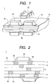
- Fig.1 is a view showing a substrate structure according to a first embodiment of the invention.
- Fig.2 is a view showing details of a section of the substrate according to the first embodiment of the invention.
- Fig.3 is a view showing a conventional substrate structure.
- the substrate structure 1 shows a substrate structure of a control substrate mounted at inside of a housing of a transmission in a vehicle for controlling the transmission.
- a substrate 10 is formed by constituting multiple layers of plate members comprising a resin material having high heat resistance such as aramid material.
- the plate members is superposed on each other,
- the substrate is formed by forming a circuit pattern on the surface of the plate member comprising the aramid material and laminating other plate member to sandwich the formed pattern therebetween.
- bonding is carried out by melting a surface of a bonded portion of the members by heat.
- the bonding method is not limited thereto but the bonding can be carried out by various methods such as using an adhering agent.
- the surface of the substrate 10 is formed with an electrically conductive part pad 40 and a mounted part 20 constituting a surface mounted part, is mounted on the part pad 40 and is mounted thereon.
- a method of mounting the mounted part 20 there is provided a method of mounting the part by coating solder paste on a portion to which the mounted part 20 is intended to mount, mounting the mounted part 20 thereon and thereafter melting the solder paste by subjecting the substrate 10 under a high temperature environment such as a reflow furnace, or coating and solidifying electrically conductive paste to thereby mount the mounted part 20.
- a through hole 30 for connecting the part pad 40 and a circuit pattern formed at an inner layer of the substrate 10 comprising the multiple layers. Further, the through hole 30 is provided also for connecting circuit patterns formed at different layers in the inner layer. Further, an electrically conductive portion 60 is formed at an inner portion of the through hole 30 in the form of filling the solder paste to thereby embed the through hole 30 and accordingly, there is constituted a shape strong at thermal stress in the vertical direction (thickness direction of substrate ).
- the through hole 30 does not penetrate an upper face and a lower face of the substrate 10 as in a through hole but is provided basically for connecting contiguous layers in the substrate 10 and accordingly, a distance in the vertical direction ( thickness of substrate ) becomes shorter than that of a through hole. Therefore, thermal stress in the vertical direction operated to the through hole 30 becomes smaller than that of a through hole.
- the part pad 40 can be formed right above the through hole 30. Therefore, in comparison with the case of forming the through hole 30 at a portion different from the part pad 40, a mounting efficiency can significantly be promoted.
- all of circuit patterns are formed at the inner portion of the substrate 10 and the surface of the substrate 10 is only provided with the part pad 40 for mounting the mounted part 20 and accordingly, arrangement of the part pad 40 formed at the surface portion of the substrate 10 can be simplified to a degree of eliminating the possibility of shortcircuiting circuits by dew condensation or the like. Therefore, the resist film for covering the part pad 40 or the like can be dispensed with and accordingly, break of the circuit pattern accompanied by break of the resist film under the high temperature environment can be prevented.
- Fig.2 is a view showing details of a section of the substrate according to the first embodiment of the invention.
- the substrate structure 1 shown in Fig.2 shows the section of the substrate 10 when 6 of layers are provided.
- ⁇ layers provided at the substrate 10 surface layers 11 exposed to respective surfaces of upper and lower faces of the substrate, are constructed by a constitution in which only the part pads 40 are formed and by a constitution in which the part pads 40 are not exposed to the surfaces by mounting the mounted parts 20 thereon by solder 50.
- the layers at the inner portion of the substrate contiguous to the surface layers 11, are a power source layer 12 and a surround layer 14, the power source layer 12 is connected to a power source and the ground layer 14 is grounded.
- the other layers sandwiched by the power source layer 12 and the ground layer 14, are circuit layers 13 which are layers for arbitrarily connecting the mounted parts 20 mounted on the surfaces of the substrate 10 with the power source layer 12 and the ground layer 14 and forming circuit patterns. Further, intervals between the respective layers of the substrate 10 are electrically connected by the through holes 30.
- the high temperature resistance of the aramid material used in the substrate 10 falls in a range of 170 through 180°C and accordingly, the aramid material is not softened even when provided at inside of a housing of a transmission ( surrounding temperature is about 120°C ).
- the linear expansion coefficient produced by heat of the substrate 10 becomes about 8 ppm in the horizontal direction ( longitudinal direction of substrate ) by forming the substrate 10 by the aramid material and accordingly, thermal stress produced in the horizontal direction becomes significantly lower than that of the substrate formed by the glass epoxy material. Further, since the thermal stress in the horizontal direction is lowered, a bare chip part 25 having an electrode at outside of the chip can be mounted to the substrate 10 as the mounted part 20.
- the aramid material is more excellent than the glass epoxy material in view of its strength and therefore, when 1.6mm is needed for the thickness of the substrate 10, for example, in the case of forming the substrate 10 by the glass epoxy material, the thickness can be restrained to 0.6 through 0.8 mm in the case of the aramid material.
- the aramid material is provided with a characteristic of low dielectric constant and therefore, by using the aramid material for the substrate 10, there is produced an effect of absorbing noise generated among the respective layers of the substrate 10.
- the substrate structure 1 in the first embodiment of the invention described above it has been confirmed by experiments that the substrate structure 1 functions normally even when the substrate structure 1 is subjected to thermal cycle of 3000 cycles between -40°C and 125°C of surrounding temperature, or even when subjected under an environment at surrounding temperature 130°C for 2000 hours.
- the substrate structure 1 according to the first embodiment of the invention is regarded to function normally even under a high temperature environment as in a housing of a transmission in a vehicle ( surrounding temperature is about 120°C ).
- the substrate structure 1 is applicable to high temperature environment and applicable even to a case in which a surrounding environment is not under a high temperature environment.
- the aramid material is used as the material of the substrate 10, as the material, any material may be used so far as the material is provided with high temperature resistance under a temperature environment of mounting the substrate.
- the substrate 10 comprises the 6 layers
- the invention is not limited thereto.
- the solder paste is filled at the inner portion of the through hole 30, further, the through hole 30 is provided such that contiguous layers are connected to each other, and the aramid material is used as the material of the substrate 10, the invention does not need to necessarily take all of these into a consideration but when sufficient resistance against thermal stress in the vertical direction under the temperature environment of mounting the substrate is achieved by carrying out at least one of these, there may be constructed a constitution taking only one of these into a consideration.
- the substrate structure in the invention there is constructed the constitution in which the substrate is formed by the resin material or the like having high temperature resistance and the resist film may not be provided on the surface of the substrate and constructed by the constitution of restraining thermal stress in the vertical direction of the substrate ( thickness direction of substrate ) and accordingly, the substrate structure capable of being mounted under the high temperature environment, can be provided at low cost.
Landscapes
- Engineering & Computer Science (AREA)
- Microelectronics & Electronic Packaging (AREA)
- Manufacturing & Machinery (AREA)
- Production Of Multi-Layered Print Wiring Board (AREA)
- Combinations Of Printed Boards (AREA)
- Printing Elements For Providing Electric Connections Between Printed Circuits (AREA)
- Structure Of Printed Boards (AREA)
Abstract
Description
an electrically conductive paste may form the electrically conducting member; and
the electrically conductive paste may be filled with in the hole to electrically connect the part pad with the electric pattern of the second substrate.
Claims (7)
- A substrate structure comprising:a plurality of substrates superposed on each other;a circuit pattern disposed between the plurality of substrates;a part pad provided on the uppermost substrate; andan electrically conducting member disposed in the substrate and right under the part pad, the electrically conducting member electrically connecting the part pad with the circuit pattern.
- A substrate structure according to claim 1, further comprising:a part mounted on the uppermost substrate, the part having an electrode, the part pad being provided on the uppermost substrate to correspond to the electrode of the part.
- The substrate structure according to claim 1 or claim 2, wherein the substrate has a hole formed right under the part pad;
an electrically conductive paste forms the electrically conducting member; and
the electrically conductive paste is filled with in the hole to electrically connect the part pad with the circuit pattern. - The substrate structure according to any of the preceding claims, wherein the plurality of substrates comprise a resin material.
- The substrate structure according to any of the preceding claims, wherein the circuit pattern comprises at least one circuit pattern; and
all of the at least one circuit pattern is formed between the plurality of substrates. - The substrate structure according to claim 5, wherein the circuit pattern comprises a plurality of circuit patterns.
- A substrate structure according to claim 6, wherein the uppermost circuit pattern is electrically connected with a battery; and
the lowermost circuit pattern is grounded.
Applications Claiming Priority (2)
| Application Number | Priority Date | Filing Date | Title |
|---|---|---|---|
| JP2000358903 | 2000-11-27 | ||
| JP2000358903A JP3857042B2 (en) | 2000-11-27 | 2000-11-27 | Board structure |
Publications (3)
| Publication Number | Publication Date |
|---|---|
| EP1209957A2 true EP1209957A2 (en) | 2002-05-29 |
| EP1209957A3 EP1209957A3 (en) | 2003-07-23 |
| EP1209957B1 EP1209957B1 (en) | 2011-02-02 |
Family
ID=18830736
Family Applications (1)
| Application Number | Title | Priority Date | Filing Date |
|---|---|---|---|
| EP01309936A Expired - Lifetime EP1209957B1 (en) | 2000-11-27 | 2001-11-27 | Substrate structure |
Country Status (5)
| Country | Link |
|---|---|
| US (1) | US6750537B2 (en) |
| EP (1) | EP1209957B1 (en) |
| JP (1) | JP3857042B2 (en) |
| CN (1) | CN1190114C (en) |
| DE (1) | DE60143981D1 (en) |
Families Citing this family (2)
| Publication number | Priority date | Publication date | Assignee | Title |
|---|---|---|---|---|
| JP2012142371A (en) * | 2010-12-28 | 2012-07-26 | Mitsubishi Electric Corp | Semiconductor package |
| JP2023043862A (en) * | 2021-09-16 | 2023-03-29 | 方略電子股▲ふん▼有限公司 | electronic device |
Family Cites Families (28)
| Publication number | Priority date | Publication date | Assignee | Title |
|---|---|---|---|---|
| DE3639443A1 (en) * | 1986-11-18 | 1988-05-26 | Ant Nachrichtentech | Printed circuit board and method for its production |
| GB8705543D0 (en) * | 1987-03-10 | 1987-04-15 | Int Computers Ltd | Printed circuit board |
| US4967314A (en) * | 1988-03-28 | 1990-10-30 | Prime Computer Inc. | Circuit board construction |
| JPH0499394A (en) * | 1990-08-17 | 1992-03-31 | Cmk Corp | Multilayer printed circuit board |
| JPH05218618A (en) | 1992-01-30 | 1993-08-27 | Cmk Corp | Method for manufacturing printed wiring board |
| JP2721093B2 (en) * | 1992-07-21 | 1998-03-04 | 三菱電機株式会社 | Semiconductor device |
| US5371403A (en) * | 1993-09-24 | 1994-12-06 | Vlsi Technology, Inc. | High performance package using high dielectric constant materials for power/ground and low dielectric constant materials for signal lines |
| JPH08116174A (en) | 1994-08-25 | 1996-05-07 | Matsushita Electric Ind Co Ltd | Circuit forming substrate and manufacturing method thereof |
| US5509200A (en) * | 1994-11-21 | 1996-04-23 | International Business Machines Corporation | Method of making laminar stackable circuit board structure |
| US5672911A (en) * | 1996-05-30 | 1997-09-30 | Lsi Logic Corporation | Apparatus to decouple core circuits power supply from input-output circuits power supply in a semiconductor device package |
| US5708296A (en) * | 1996-06-24 | 1998-01-13 | Intel Corporation | Power-ground plane for a C4 flip-chip substrate |
| DE19642929A1 (en) | 1996-10-17 | 1997-07-17 | Siemens Ag | Multi-layered printed circuit board with HF component |
| EP0943157A4 (en) * | 1996-10-31 | 2000-05-24 | Sarnoff Corp | Integrated electronic circuit |
| JPH10284838A (en) | 1997-04-01 | 1998-10-23 | Murata Mfg Co Ltd | Multilayer circuit board and its mounting method |
| US5847936A (en) * | 1997-06-20 | 1998-12-08 | Sun Microsystems, Inc. | Optimized routing scheme for an integrated circuit/printed circuit board |
| JP4099837B2 (en) | 1997-08-27 | 2008-06-11 | 株式会社村田製作所 | Low temperature fired ceramic multilayer substrate manufacturing method |
| USRE41242E1 (en) * | 1997-10-17 | 2010-04-20 | Ibiden Co., Ltd. | Package substrate |
| WO1999034654A1 (en) * | 1997-12-29 | 1999-07-08 | Ibiden Co., Ltd. | Multilayer printed wiring board |
| US5898217A (en) * | 1998-01-05 | 1999-04-27 | Motorola, Inc. | Semiconductor device including a substrate having clustered interconnects |
| US6064113A (en) * | 1998-01-13 | 2000-05-16 | Lsi Logic Corporation | Semiconductor device package including a substrate having bonding fingers within an electrically conductive ring surrounding a die area and a combined power and ground plane to stabilize signal path impedances |
| US6008534A (en) * | 1998-01-14 | 1999-12-28 | Lsi Logic Corporation | Integrated circuit package having signal traces interposed between power and ground conductors in order to form stripline transmission lines |
| US6187652B1 (en) * | 1998-09-14 | 2001-02-13 | Fujitsu Limited | Method of fabrication of multiple-layer high density substrate |
| JP2000100985A (en) * | 1998-09-17 | 2000-04-07 | Nitto Denko Corp | Substrate for mounting semiconductor element, method of manufacturing the same, and application |
| US6239485B1 (en) * | 1998-11-13 | 2001-05-29 | Fujitsu Limited | Reduced cross-talk noise high density signal interposer with power and ground wrap |
| US6413620B1 (en) * | 1999-06-30 | 2002-07-02 | Kyocera Corporation | Ceramic wiring substrate and method of producing the same |
| US6137161A (en) * | 1999-09-14 | 2000-10-24 | International Business Machines Corporation | Interposer array module for capacitive decoupling and filtering |
| JP2001168125A (en) * | 1999-12-03 | 2001-06-22 | Nec Corp | Semiconductor device |
| US6388207B1 (en) * | 2000-12-29 | 2002-05-14 | Intel Corporation | Electronic assembly with trench structures and methods of manufacture |
-
2000
- 2000-11-27 JP JP2000358903A patent/JP3857042B2/en not_active Expired - Fee Related
-
2001
- 2001-11-27 CN CNB011397039A patent/CN1190114C/en not_active Expired - Fee Related
- 2001-11-27 EP EP01309936A patent/EP1209957B1/en not_active Expired - Lifetime
- 2001-11-27 US US09/993,561 patent/US6750537B2/en not_active Expired - Fee Related
- 2001-11-27 DE DE60143981T patent/DE60143981D1/en not_active Expired - Lifetime
Also Published As
| Publication number | Publication date |
|---|---|
| JP2002164666A (en) | 2002-06-07 |
| CN1190114C (en) | 2005-02-16 |
| US20020063325A1 (en) | 2002-05-30 |
| JP3857042B2 (en) | 2006-12-13 |
| EP1209957A3 (en) | 2003-07-23 |
| CN1356862A (en) | 2002-07-03 |
| US6750537B2 (en) | 2004-06-15 |
| DE60143981D1 (en) | 2011-03-17 |
| EP1209957B1 (en) | 2011-02-02 |
Similar Documents
| Publication | Publication Date | Title |
|---|---|---|
| US7365416B2 (en) | Multi-level semiconductor module and method for fabricating the same | |
| US6930257B1 (en) | Integrated circuit substrate having laminated laser-embedded circuit layers | |
| EP0052920B1 (en) | Electronic circuit interconnection system | |
| JP4205749B2 (en) | Electronic module manufacturing method and electronic module | |
| CN103339726B (en) | Electronic device, method for producing the latter, and printed circuit board comprising electronic device | |
| JP3401767B2 (en) | Multilayer ceramic substrate and method of manufacturing the same | |
| JP2790122B2 (en) | Laminated circuit board | |
| US7929316B2 (en) | Composite electronic component | |
| US6449168B1 (en) | Circuit board and a method for manufacturing the same | |
| US20090002950A1 (en) | Multi-layer electrically isolated thermal conduction structure for a circuit board assembly | |
| US8302277B2 (en) | Module and manufacturing method thereof | |
| CN1332598A (en) | Printed-wiring board with cavity for mounting electronic component and manufacture thereof | |
| CA2024784C (en) | Stackable multilayer substrate for mounting integrated circuits | |
| JP2008016844A (en) | Printed circuit board and manufacturing method thereof | |
| US7288728B2 (en) | Electronic package and packaging method | |
| US20080257584A1 (en) | Multilayer wiring board | |
| CN100472780C (en) | Electronic component and its manufacturing method | |
| US6750537B2 (en) | Substrate structure | |
| US5094969A (en) | Method for making a stackable multilayer substrate for mounting integrated circuits | |
| JPH08236940A (en) | Multilayered wiring board | |
| JPH11112114A (en) | Printed board | |
| WO2012165111A1 (en) | Method for producing multi-layer substrate and multi-layer substrate | |
| KR20170134250A (en) | Layered type substrate and method for producing the same | |
| EP0967650A2 (en) | Circuit board for mounting bare chip | |
| JP2787238B2 (en) | Film carrier with printing element |
Legal Events
| Date | Code | Title | Description |
|---|---|---|---|
| PUAI | Public reference made under article 153(3) epc to a published international application that has entered the european phase |
Free format text: ORIGINAL CODE: 0009012 |
|
| AK | Designated contracting states |
Kind code of ref document: A2 Designated state(s): AT BE CH CY DE DK ES FI FR GB GR IE IT LI LU MC NL PT SE TR |
|
| AX | Request for extension of the european patent |
Free format text: AL;LT;LV;MK;RO;SI |
|
| PUAL | Search report despatched |
Free format text: ORIGINAL CODE: 0009013 |
|
| AK | Designated contracting states |
Designated state(s): AT BE CH CY DE DK ES FI FR GB GR IE IT LI LU MC NL PT SE TR |
|
| AX | Request for extension of the european patent |
Extension state: AL LT LV MK RO SI |
|
| 17P | Request for examination filed |
Effective date: 20040113 |
|
| AKX | Designation fees paid |
Designated state(s): DE FR GB |
|
| 17Q | First examination report despatched |
Effective date: 20080903 |
|
| GRAP | Despatch of communication of intention to grant a patent |
Free format text: ORIGINAL CODE: EPIDOSNIGR1 |
|
| GRAC | Information related to communication of intention to grant a patent modified |
Free format text: ORIGINAL CODE: EPIDOSCIGR1 |
|
| GRAS | Grant fee paid |
Free format text: ORIGINAL CODE: EPIDOSNIGR3 |
|
| GRAA | (expected) grant |
Free format text: ORIGINAL CODE: 0009210 |
|
| AK | Designated contracting states |
Kind code of ref document: B1 Designated state(s): DE FR GB |
|
| REG | Reference to a national code |
Ref country code: GB Ref legal event code: FG4D |
|
| REF | Corresponds to: |
Ref document number: 60143981 Country of ref document: DE Date of ref document: 20110317 Kind code of ref document: P |
|
| REG | Reference to a national code |
Ref country code: DE Ref legal event code: R096 Ref document number: 60143981 Country of ref document: DE Effective date: 20110317 |
|
| PLBE | No opposition filed within time limit |
Free format text: ORIGINAL CODE: 0009261 |
|
| STAA | Information on the status of an ep patent application or granted ep patent |
Free format text: STATUS: NO OPPOSITION FILED WITHIN TIME LIMIT |
|
| 26N | No opposition filed |
Effective date: 20111103 |
|
| REG | Reference to a national code |
Ref country code: DE Ref legal event code: R097 Ref document number: 60143981 Country of ref document: DE Effective date: 20111103 |
|
| REG | Reference to a national code |
Ref country code: FR Ref legal event code: PLFP Year of fee payment: 15 |
|
| REG | Reference to a national code |
Ref country code: FR Ref legal event code: PLFP Year of fee payment: 16 |
|
| REG | Reference to a national code |
Ref country code: FR Ref legal event code: PLFP Year of fee payment: 17 |
|
| PGFP | Annual fee paid to national office [announced via postgrant information from national office to epo] |
Ref country code: FR Payment date: 20171012 Year of fee payment: 17 Ref country code: DE Payment date: 20171121 Year of fee payment: 17 |
|
| PGFP | Annual fee paid to national office [announced via postgrant information from national office to epo] |
Ref country code: GB Payment date: 20171122 Year of fee payment: 17 |
|
| REG | Reference to a national code |
Ref country code: DE Ref legal event code: R119 Ref document number: 60143981 Country of ref document: DE |
|
| GBPC | Gb: european patent ceased through non-payment of renewal fee |
Effective date: 20181127 |
|
| PG25 | Lapsed in a contracting state [announced via postgrant information from national office to epo] |
Ref country code: FR Free format text: LAPSE BECAUSE OF NON-PAYMENT OF DUE FEES Effective date: 20181130 Ref country code: DE Free format text: LAPSE BECAUSE OF NON-PAYMENT OF DUE FEES Effective date: 20190601 |
|
| PG25 | Lapsed in a contracting state [announced via postgrant information from national office to epo] |
Ref country code: GB Free format text: LAPSE BECAUSE OF NON-PAYMENT OF DUE FEES Effective date: 20181127 |