EP1208645B1 - Circuit configuration for generating square wave pulses - Google Patents
Circuit configuration for generating square wave pulses Download PDFInfo
- Publication number
- EP1208645B1 EP1208645B1 EP01956405A EP01956405A EP1208645B1 EP 1208645 B1 EP1208645 B1 EP 1208645B1 EP 01956405 A EP01956405 A EP 01956405A EP 01956405 A EP01956405 A EP 01956405A EP 1208645 B1 EP1208645 B1 EP 1208645B1
- Authority
- EP
- European Patent Office
- Prior art keywords
- comparator
- circuit configuration
- flip
- flop
- energy storage
- Prior art date
- Legal status (The legal status is an assumption and is not a legal conclusion. Google has not performed a legal analysis and makes no representation as to the accuracy of the status listed.)
- Expired - Lifetime
Links
Images

Classifications
-
- H—ELECTRICITY
- H03—ELECTRONIC CIRCUITRY
- H03K—PULSE TECHNIQUE
- H03K3/00—Circuits for generating electric pulses; Monostable, bistable or multistable circuits
- H03K3/02—Generators characterised by the type of circuit or by the means used for producing pulses
- H03K3/023—Generators characterised by the type of circuit or by the means used for producing pulses by the use of differential amplifiers or comparators, with internal or external positive feedback
- H03K3/0231—Astable circuits
-
- H—ELECTRICITY
- H03—ELECTRONIC CIRCUITRY
- H03K—PULSE TECHNIQUE
- H03K17/00—Electronic switching or gating, i.e. not by contact-making and –breaking
- H03K17/51—Electronic switching or gating, i.e. not by contact-making and –breaking characterised by the components used
- H03K17/56—Electronic switching or gating, i.e. not by contact-making and –breaking characterised by the components used by the use, as active elements, of semiconductor devices
- H03K17/687—Electronic switching or gating, i.e. not by contact-making and –breaking characterised by the components used by the use, as active elements, of semiconductor devices the devices being field-effect transistors
- H03K17/6871—Electronic switching or gating, i.e. not by contact-making and –breaking characterised by the components used by the use, as active elements, of semiconductor devices the devices being field-effect transistors the output circuit comprising more than one controlled field-effect transistor
- H03K17/6872—Electronic switching or gating, i.e. not by contact-making and –breaking characterised by the components used by the use, as active elements, of semiconductor devices the devices being field-effect transistors the output circuit comprising more than one controlled field-effect transistor using complementary field-effect transistors
-
- H—ELECTRICITY
- H03—ELECTRONIC CIRCUITRY
- H03K—PULSE TECHNIQUE
- H03K3/00—Circuits for generating electric pulses; Monostable, bistable or multistable circuits
- H03K3/02—Generators characterised by the type of circuit or by the means used for producing pulses
- H03K3/353—Generators characterised by the type of circuit or by the means used for producing pulses by the use, as active elements, of field-effect transistors with internal or external positive feedback
- H03K3/354—Astable circuits
Definitions
- the invention relates to a circuit arrangement for generating of square pulses, with an edge-triggered flip-flop and at least one comparator whose output is connected to the trigger input the flip-flop is connected, as well as a Energy storage element, which depends on the Switching state of the flip-flop is charged alternately, wherein in series with the energy storage element at least one Switching threshold is connected, on which one of generated by the energy storage element flowing current Voltage drops which affect the signal input of the comparator is given.
- the well-known circuit is for example, to measure the field strength of a magnetic field used.
- This is a magnetic field probe, which is called inductance is formed and the energy storage element, in the introduced to be measured magnetic field.
- the magnetic field probe is like that designed to be characterized by the magnetic field to be measured and the Magnetic field generated by the current brought to saturation becomes. As long as the magnetic field probe no external magnetic field acts, that is, the magnetic field to be measured is zero has the magnetic field probe in relation to one through it electric current flowing in from the direction of the Electricity independent electrical behavior. At the of the Circuit arrangement generated square pulses thus arises a duty cycle of 1 to 1.
- a known circuit arrangement is shown in FIG.
- the known circuit arrangement are two comparators provided whose outputs go to an AND gate whose Output is connected to the trigger input of the flip-flop.
- the Signal inputs of the comparators are each with a different one End of the energy storage, that is the magnetic field probe, connected.
- the energy storage is between the two outputs the flip-flop switched. Thus, depending on the position of the Flip flops in different directions current through the Energy storage.
- Between the outputs of the flip-flop and the Energy storage are each switching threshold resistances connected.
- the junctions of the Switching threshold resistors and the energy storage are respectively connected to the signal input of a comparator.
- the two Reference inputs of the comparators are connected to each other, so that the same reference voltage is present at both comparators.
- the known circuit has the disadvantage that the Tolerances of the switching threshold resistances as well as the tolerances the switching thresholds of the comparators on the duty cycle impact.
- different effects Delay times of the comparators disadvantageous to a Symmetry of the circuit arrangement.
- the affects Running time of the AND gate disadvantageous to the circuit reached resolution.
- caused by the Use of an AND gate further costs.
- a circuit arrangement for generating of square pulses with an edge-triggered flip-flop and at least one comparator whose output is connected to the Trigger input of the flip-flop is connected, as well as a Energy storage element, which depends on the Switching state of the flip-flop is charged alternately, wherein in series with the energy storage element at least one Switching threshold is connected, on which one of generated by the energy storage element flowing current Voltage drops which affect the signal input of the comparator is given, characterized in that the Energy storage element is arranged in the transverse branch of a bridge, arranged in each of the four bridge sections a switch is, with the switches in pairs crossed by the Flip-flop are switched, so that the current flow in the shunt branch is reversible, and that the bridge with the Switching threshold resistor is connected in series, the Junction of the bridge with the switching threshold resistance is connected to the signal input of the comparator.
- the inventive arrangement is in an advantageous manner avoided that two switching threshold resistances required are. This reduces the space required, and second, by using only one Switching threshold resistance asymmetries avoided. Because, that the current flowing through the energy storage is always through the same switching threshold resistance flows, the affects Tolerance of switching threshold resistance in both Switching states of the flip-flop equal.
- an embodiment of the Invention exposed in which the energy storage element is an inductance Because by that Energy storage element is an inductor, it can be as Form magnetic field probe, as in another particular embodiment of the invention is provided.
- the inductance as a magnetic field probe can be the inventive circuit arrangement in a particularly advantageous Use way to measure a magnetic field.
- the magnetic field probe for Detecting the magnetic field of a core of a Compensating current sensor is used, as in another particular embodiment of the invention is provided.
- the circuit arrangement according to the invention in a compensation current sensor can be easily the Improve the accuracy of the compensation current sensor.
- Comparator is designed as a digital gate. This leaves the circuit can be made very cheaply.
- a digital gate For example, an AND gate could be used. It has but also proved to be advantageous an analog comparator use, which provides as output signals digital signals, the are easy to process.
- the switch as a MOS-FET of which two are direct and two over inverters the outputs of the flip-flop are controlled.
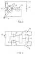
- FIG. 1 shows an embodiment of the invention Circuit arrangement in a schematic representation
- Fig. 2 a Compensating current sensor in a schematic representation
- Fig. 3rd a circuit arrangement according to the prior art in schematic representation.
- a coil 3 and a series resistor 11 connected in series with it are arranged in the transverse branch of a bridge.
- each formed as a MOS-FET switch 7, 8, 9, 10 is arranged in the four bridge sections of the bridge.
- the arranged in a part of the bridge first switch 7 and the second switch 8 are formed as a P-channel MOS-FET and connected to the operating voltage V cc .
- the arranged in the other part of the bridge third switch 9 and the fourth switch 10 are formed as N-channel MOS-FET and connected to a switching threshold resistor 4. The other end of the switching threshold resistor 4 is connected to ground.
- the junction between the N-channel MOS-FET 9, 10 and the switching threshold resistor 4 is connected to the signal input 2 a of a comparator 2.
- a comparator 2 At the reference input 2b of the comparator 2 is applied to a reference voltage U ref .
- the output of the comparator 2 is connected to the trigger input of an edge-triggered flip-flop 1.
- the non-inverting output 1a of the flip-flop 1 is connected via a first inverter 5 to the gate of the first P-channel MOS-FET 7, as well as directly connected to the gate of the cross-arranged in the bridge fourth N-channel MOS-FET 10 ,
- the inverting output 1b of the flip-flop 1 is connected via a second inverter 6 to the gate of the second P-channel MOS-FET 8, as well as directly connected to the gate of the cross-arranged in the bridge third N-channel MOS-FET 9.
- the MOSFETs 7, 8, 9, 10 are thus switched through in pairs (7 and 10 or 8 and 9) by the flip-flop 1.
- Is the non-inverting output 1a of the flip-flop 1 the Output voltage are the first MOS-FET 7 and the fourth MOS-FET 10 through. It can thus be a current from the left to the right through in the transverse branch of the bridge, that is through the Series resistor 11 and the inductor 3 flow.
- the comparator 2 is for example an analog comparator, the at its output provides a digital signal that in the downstream digital circuit can be easily processed can.
- a comparator 2 for example, as a Digital gate configured component can be used optionally with a correspondingly adapted Circuit design.
- a field probe 12 is arranged in the air gap of a toroidal core 13 which encloses a conductor 15 whose current is to be measured.
- the field probe 12 is designed as an inductance, which passes through the magnetic field in the air gap of the ring core 13 in the saturation.
- the field probe 12 represents the inductance 3 contained in FIG. 1 and is arranged in a circuit arrangement corresponding to FIG. 1, which forms part of a controller 16.
- the pulse duty factor of the square-wave pulses generated by the magnetic field in the air gap of the ring core 13 is evaluated in the controller 16 and used to generate a compensation current I A.
- the compensation current I A is passed through a coil 14 which is wound around the ring core 13.
- the controller 16 is designed so that the current flowing through the coil 14 is so large that the magnetic field in the air gap of the toroidal core 13 is almost zero. As a result, the current I A flowing through the coil 14 can be taken as a measure of the current flowing through the conductor 15.
- a resistor 17 is connected in series with the coil 14, at which the output voltage U A drops.
Description
Die Erfindung betrifft eine Schaltungsanordnung zur Erzeugung von Rechteckimpulsen, mit einem flankengetriggerten Flip-Flop und wenigstens einem Komparator, dessen Ausgang mit dem Triggereingang des Flip-Flops verbunden ist, sowie einem Energiespeicherelement, welches in Abhängigkeit des Schaltzustandes des Flip-Flops wechselseitig aufgeladen wird, wobei in Reihe mit dem Energiespeicherelement wenigstens ein Schaltschwellenwiderstand geschaltet ist, an welchem eine vom durch das Energiespeicherelement fließenden Strom erzeugte Spannung abfällt, welche auf den Signaleingang des Komparators gegeben wird.The invention relates to a circuit arrangement for generating of square pulses, with an edge-triggered flip-flop and at least one comparator whose output is connected to the trigger input the flip-flop is connected, as well as a Energy storage element, which depends on the Switching state of the flip-flop is charged alternately, wherein in series with the energy storage element at least one Switching threshold is connected, on which one of generated by the energy storage element flowing current Voltage drops which affect the signal input of the comparator is given.
Es ist bekannt, eine derartige Schaltungsanordnung zur Erzeugung von Rechteckimpulsen zu verwenden. Die bekannte Schaltung wird beispielsweise zur Messung der Feldstärke eines Magnetfeldes verwendet. Dabei wird eine Magnetfeldsonde, die als Induktivität ausgebildet ist und das Energiespeicherelement darstellt, in das zu messende Magnetfeld eingebracht. Die Magnetfeldsonde ist so ausgebildet, daß sie durch das zu messende Magnetfeld und das durch den Strom erzeugte Magnetfeld in die Sättigung gebracht wird. Solange auf die Magnetfeldsonde kein äußeres Magnetfeld einwirkt, das heißt, das zu messende Magnetfeld Null ist, hat die Magnetfeldsonde in Bezug auf einen durch sie hindurchfließenden elektrischen Strom ein von der Richtung des Stroms unabhängiges elektrisches Verhalten. Bei den von der Schaltungsanordnung erzeugten Rechteckimpulsen stellt sich somit ein Tastverhältnis von 1 zu 1 ein.It is known, such a circuit arrangement for generating of rectangular pulses to use. The well-known circuit is for example, to measure the field strength of a magnetic field used. This is a magnetic field probe, which is called inductance is formed and the energy storage element, in the introduced to be measured magnetic field. The magnetic field probe is like that designed to be characterized by the magnetic field to be measured and the Magnetic field generated by the current brought to saturation becomes. As long as the magnetic field probe no external magnetic field acts, that is, the magnetic field to be measured is zero has the magnetic field probe in relation to one through it electric current flowing in from the direction of the Electricity independent electrical behavior. At the of the Circuit arrangement generated square pulses thus arises a duty cycle of 1 to 1.
Wirkt auf die Magnetfeldsonde ein äußeres Magnetfeld ein, das heißt, ist das zu messende Magnetfeld nicht mehr Null, gelangt die Magnetfeldsonde in einer Richtung früher in die Sättigung, als in der anderen. Bezüglich eines durch sie hindurchfließenden elektrischen Stromes ist ihr Verhalten daher nicht mehr von der Richtung des elektrischen Stromes unabhängig. Hierdurch ändert sich das Tastverhältnis der Rechteckimpulse. Das Tastverhältnis der Rechteckimpulse stellt somit ein Maß für das auf die Magnetfeldsonde einwirkende magnetische Feld dar.Acts on the magnetic field probe an external magnetic field, the means that the magnetic field to be measured is no longer zero the magnetic field probe in one direction earlier into saturation, than in the other. Regarding a flowing through them Electricity is therefore no longer their behavior Direction of the electric current independently. This changes the duty cycle of the rectangular pulses. The duty cycle The square pulses thus provides a measure of that on the Magnetic field magnetic field acting.
Eine bekannte Schaltungsanordnung ist in Figur 3 dargestellt. Bei der bekannten Schaltungsanordnung sind zwei Komparatoren vorgesehen, deren Ausgänge auf ein UND-Gatter gehen, dessen Ausgang mit dem Triggereingang des Flip-Flops verbunden ist. Die Signaleingänge der Komparatoren sind jeweils mit einem anderen Ende des Energiespeichers, das heißt der Magnetfeldsonde, verbunden. Der Energiespeicher ist zwischen die beiden Ausgänge des Flip-Flops geschaltet. Somit fließt je nach Stellung des Flip-Flops in unterschiedlicher Richtung Strom durch den Energiespeicher. Zwischen den Ausgängen des Flip-Flops und dem Energiespeicher sind jeweils Schaltschwellenwiderstände geschaltet. Die Verbindungsstellen der Schaltschwellenwiderstände und dem Energiespeicher sind jeweils mit dem Signaleingang eines Komparators verbunden. Die beiden Referenzeingänge der Komparatoren sind miteinander verbunden, so daß an beiden Komparatoren dieselbe Referenzspannung anliegt. A known circuit arrangement is shown in FIG. In the known circuit arrangement are two comparators provided whose outputs go to an AND gate whose Output is connected to the trigger input of the flip-flop. The Signal inputs of the comparators are each with a different one End of the energy storage, that is the magnetic field probe, connected. The energy storage is between the two outputs the flip-flop switched. Thus, depending on the position of the Flip flops in different directions current through the Energy storage. Between the outputs of the flip-flop and the Energy storage are each switching threshold resistances connected. The junctions of the Switching threshold resistors and the energy storage are respectively connected to the signal input of a comparator. The two Reference inputs of the comparators are connected to each other, so that the same reference voltage is present at both comparators.
Nach einem Umschalten des Flip-Flops liegt an dem Ausgang des Flip-Flops, an dem keine Ausgangsspannung anlag, nunmehr Ausgangsspannung an und an dem anderen Ausgang nicht mehr. Durch die in der Spule gespeicherte Energie wird der ursprüngliche Stromfluß jedoch aufrechterhalten. Hierdurch sinkt das Potential am Signaleingang des betreffenden Komparators unter die Schaltschwelle. Dies hat zur Folge, daß die Spannung am Ausgang des betreffenden Komparators Null wird. Hierdurch wird auch der Ausgang des UND-Gatters Null. so daß die Spannung am Signaleingang des betreffenden Komparators wieder die Schaltschwelle erreicht, wodurch der Komparator wieder ein Ausgangssignal abgibt, und das UND-Gatter durchschaltet. Durch die beim Schalten des UND-Gatters entstehende Flanke wird das Flip-Flop wieder getriggert, so daß es erneut umschaltet, und sich der soeben beschriebene Vorgang wiederholt. Die Schaltung ist so dimensioniert, daß sie mit einer Frequenz von etwa 350 Kilohertz schwingt.After switching the flip-flop is located at the output of Flip-flops, to which no output voltage applied, now Output voltage on and at the other output no longer. By the energy stored in the coil becomes the original one Maintained current flow, however. This reduces the potential at the signal input of the relevant comparator under the Switching threshold. This has the consequence that the voltage at the output of the relevant comparator becomes zero. This will also the Output of the AND gate zero. so that the voltage at Signal input of the relevant comparator again Switching threshold reached, causing the comparator again Output signal, and the AND gate turns on. By the resulting when switching the AND gate edge is the Flip-flop triggered again, so that it switches again, and the process just described is repeated. The circuit is dimensioned to be at a frequency of about 350 Kilohertz is swinging.
Die bekannte Schaltung hat jedoch den Nachteil, daß sich die Toleranzen der Schaltschwellenwiderstände sowie die Toleranzen der Schaltschwellen der Komparatoren auf das Tastverhältnis auswirken. Darüber hinaus wirken sich unterschiedliche Verzögerungszeiten der Komparatoren nachteilig auf eine Symmetrie der Schaltungsanordnung aus. Auch wirkt sich die Laufzeit des UND-Gatters nachteilig auf die mit der Schaltung erreichte Auflösung aus. Darüber hinaus entstehen durch die Verwendung eines UND-Gatters weitere Kosten.However, the known circuit has the disadvantage that the Tolerances of the switching threshold resistances as well as the tolerances the switching thresholds of the comparators on the duty cycle impact. In addition, different effects Delay times of the comparators disadvantageous to a Symmetry of the circuit arrangement. Also, the affects Running time of the AND gate disadvantageous to the circuit reached resolution. In addition, caused by the Use of an AND gate further costs.
Es ist Aufgabe der Erfindung, eine eingangs genannte Schaltungsanordnung derart auszubilden, daß der Einfluß der Toleranz der Bauelemente reduziert wird.It is an object of the invention, an aforementioned Form circuit arrangement such that the influence of Tolerance of the components is reduced.
Die Lösung dieser Aufgabe ergibt sich aus den Merkmalen des kennzeichnenden Teils des Anspruchs 1. Vorteilhafte Weiterbildungen der Erfindung ergeben sich aus den Unteransprüchen.The solution to this problem arises from the characteristics of characterizing part of claim 1. Advantageous Further developments of the invention will become apparent from the Dependent claims.
Gemäß der Erfindung ist eine Schaltungsanordnung zur Erzeugung von Rechteckimpulsen, mit einem flankengetriggerten Flip-Flop und wenigstens einem Komparator, dessen Ausgang mit dem Triggereingang des Flip-Flops verbunden ist, sowie einem Energiespeicherelement, welches in Abhängigkeit des Schaltzustandes des Flip-Flops wechselseitig aufgeladen wird, wobei in Reihe mit dem Energiespeicherelement wenigstens ein Schaltschwellenwiderstand geschaltet ist, an welchem eine vom durch das Energiespeicherelement fließenden Strom erzeugte Spannung abfällt, welche auf den Signaleingang des Komparators gegeben wird, dadurch gekennzeichnet, daß das Energiespeicherelement im Querzweig einer Brücke angeordnet ist, in deren vier Brückenabschnitten jeweils ein Schalter angeordnet ist, wobei die Schalter jeweils paarweise überkreuz von dem Flip-Flop geschaltet werden, so daß der Stromfluß im Querzweig umkehrbar ist, und daß die Brücke mit dem Schaltschwellenwiderstand in Reihe geschaltet ist, wobei die Verbindungsstelle der Brücke mit dem Schaltschwellenwiderstand mit dem Signaleingang des Komparators verbunden ist.According to the invention, a circuit arrangement for generating of square pulses, with an edge-triggered flip-flop and at least one comparator whose output is connected to the Trigger input of the flip-flop is connected, as well as a Energy storage element, which depends on the Switching state of the flip-flop is charged alternately, wherein in series with the energy storage element at least one Switching threshold is connected, on which one of generated by the energy storage element flowing current Voltage drops which affect the signal input of the comparator is given, characterized in that the Energy storage element is arranged in the transverse branch of a bridge, arranged in each of the four bridge sections a switch is, with the switches in pairs crossed by the Flip-flop are switched, so that the current flow in the shunt branch is reversible, and that the bridge with the Switching threshold resistor is connected in series, the Junction of the bridge with the switching threshold resistance is connected to the signal input of the comparator.
Durch die erfindungsgemäße Anordnung wird in vorteilhafter Weise vermieden, daß zwei Schaltschwellenwiderstände erforderlich sind. Hierdurch reduziert sich zum einen der benötigte Platz, und zum anderen werden durch die Verwendung nur eines Schaltschwellenwiderstands Asymmetrien vermieden. Denn dadurch, daß der durch den Energiespeicher fließende Strom immer durch denselben Schaltschwellenwiderstand fließt, wirkt sich die Toleranz des Schaltschwellenwiderstands in beiden Schaltzuständen des Flip-Flops gleich aus. The inventive arrangement is in an advantageous manner avoided that two switching threshold resistances required are. This reduces the space required, and second, by using only one Switching threshold resistance asymmetries avoided. Because, that the current flowing through the energy storage is always through the same switching threshold resistance flows, the affects Tolerance of switching threshold resistance in both Switching states of the flip-flop equal.
Dasselbe gilt auch für eine Toleranz des Komparators. Da nur ein Komparator verwendet wird, wirken sich Toleranzen bezüglich der Schaltschwelle und der Durchlaufzeit in beiden Schaltzuständen des Flip-Flops gleich aus. Des weiteren wird durch die Verwendung nur eines Komparators Platz und Kosten gespart.The same applies to a tolerance of the comparator. Since only one Comparator is used, tolerances affect the Switching threshold and the cycle time in both switching states equal to the flip-flop. Furthermore, by the Using only one comparator saves space and costs.
Da in der erfindungsgemäßen Schaltungsanordnung kein UND-Gatter mehr erforderlich ist, können sich hierdurch bedingte Laufzeiten nicht auswirken. Ebenso ergibt sich in vorteilhafter Weise durch den Wegfall des UND-Gatters eine Platzeinsparung.As in the circuit arrangement according to the invention no AND gate more is required, this may result in maturities do not affect. Likewise, results in an advantageous manner the omission of the AND gate a space saving.
Als besonders vorteilhaft hat sich eine Ausführungsform der Erfindung herausgestellt, bei der das Energiespeicherelement eine Induktivität ist. Denn dadurch, daß das Energiespeicherelement eine Induktivität ist, läßt es sich als Magnetfeldsonde ausbilden, wie dies bei einer weiteren besonderen Ausführungsform der Erfindung vorgesehen ist. Bei der Ausbildung der Induktivität als Magnetfeldsonde läßt sich die erfindungsgemäße Schaltungsanordnung in besonders vorteilhafter Weise zur Messung eines Magnetfeldes verwenden.To be particularly advantageous, an embodiment of the Invention exposed in which the energy storage element is an inductance. Because by that Energy storage element is an inductor, it can be as Form magnetic field probe, as in another particular embodiment of the invention is provided. In the Forming the inductance as a magnetic field probe can be the inventive circuit arrangement in a particularly advantageous Use way to measure a magnetic field.
Besonders vorteilhaft ist es, wenn die Magnetfeldsonde zur Erfassung des Magnetfeldes eines Kerns eines Kompensationsstromsensors dient, wie dies bei einer weiteren besonderen Ausführungsform der Erfindung vorgesehen ist. Durch die Verwendung der erfindungsgemäßen Schaltungsanordnung in einem Kompensationsstromsensor, läßt sich auf einfache Weise die Genauigkeit des Kompensationsstromsensors verbessern.It is particularly advantageous if the magnetic field probe for Detecting the magnetic field of a core of a Compensating current sensor is used, as in another particular embodiment of the invention is provided. By the use of the circuit arrangement according to the invention in a compensation current sensor, can be easily the Improve the accuracy of the compensation current sensor.
In einer vorteilhaften Ausgestaltung der Erfindung ist der der Komparator als Digital-Gatter ausgebildet ist. Hierdurch läßt sich die Schaltung sehr preiswert herstellen. Als Digital-Gatter könnte beispielsweise ein UND-Gatter verwendet werden. Es hat sich aber auch als vorteilhaft erwiesen einen Analog-Komparator einzusetzen, der als Ausgangssignale Digitalsignale liefert, die einfach weiterverarbeitbar sind.In an advantageous embodiment of the invention is the of Comparator is designed as a digital gate. This leaves the circuit can be made very cheaply. As a digital gate For example, an AND gate could be used. It has but also proved to be advantageous an analog comparator use, which provides as output signals digital signals, the are easy to process.
Bei einer weiteren besonderen Ausführungsform der Erfindung ist in vorteilhafter Weise vorgesehen, die Schalter als MOS-FET auszubilden, von denen zwei direkt und zwei über Inverter von den Ausgängen des Flip-Flops angesteuert werden. Durch die Ausbildung der Schalter als MOS-FET läßt sich die erfindungsgemäße Schaltungsanordnung auf einfache Weise realisieren. Darüber hinaus vereinfacht sich die Ansteuerung der Schalter. Des weiteren können die Schalter sehr präzise angesteuert werden.In a further particular embodiment of the invention provided in an advantageous manner, the switch as a MOS-FET of which two are direct and two over inverters the outputs of the flip-flop are controlled. By the Training the switch as MOS-FET can be the inventive circuit arrangement in a simple manner realize. In addition, the control of the simplifies Switch. Furthermore, the switches can be very precise be controlled.
Darüber hinaus hat sich herausgestellt, daß es besonders vorteilhaft ist, wenn im Querzweig der Brücke in Reihe mit dem Energiespeicherelement ein Vorwiderstand geschaltet ist. Durch den Vorwiderstand läßt sich auf einfache Weise die Empfindlichkeit der Schaltungsanordnung einstellen.In addition, it has been found that it is especially is advantageous if in the transverse branch of the bridge in series with the Energy storage element is connected to a resistor. By the series resistor can be easily the Adjust the sensitivity of the circuit.
Weitere Einzelheiten, Merkmale und Vorteile der vorliegenden Erfindung ergeben sich aus der nachfolgenden Beschreibung eines besonderen Ausführungsbeispiels unter Bezugnahme auf die Zeichnung.Further details, features and advantages of the present Invention will become apparent from the following description of a particular embodiment with reference to the Drawing.
Es zeigt: Fig. 1 eine Ausführungsform der erfindungsgemäßen Schaltungsanordnung in schematischer Darstellung, Fig. 2 einen Kompensationsstromsensor in schematischer Darstellung und Fig. 3 eine Schaltungsanordnung nach dem Stand der Technik in schematischer Darstellung. 1 shows an embodiment of the invention Circuit arrangement in a schematic representation, Fig. 2 a Compensating current sensor in a schematic representation and Fig. 3rd a circuit arrangement according to the prior art in schematic representation.
Wie Figur 1 entnommen werden kann, ist im Querzweig einer Brücke
eine Spule 3 sowie ein mit ihr in Reihe geschalteter
Vorwiderstand 11 angeordnet. In den vier Brückenabschnitten der
Brücke ist jeweils ein als MOS-FET ausgebildeter Schalter 7, 8,
9, 10 angeordnet. Der in einem Teil der Brücke angeordnete erste
Schalter 7 und der zweite Schalter 8 sind als P-Kanal MOS-FET
ausgebildet und mit der Betriebsspannung Vcc verbunden. Der im
anderen Teil der Brücke angeordnete dritte Schalter 9 und der
vierte Schalter 10 sind als N-Kanal MOS-FET ausgebildet und mit
einem Schaltschwellenwiderstand 4 verbunden. Das andere Ende des
Schaltschwellenwiderstands 4 ist mit Masse verbunden.As can be seen from FIG. 1, a coil 3 and a
Die Verbindungsstelle zwischen den N-Kanal MOS-FET 9, 10 und dem
Schaltschwellenwiderstand 4 ist mit dem Signaleingang 2a eines
Komparators 2 verbunden. Am Referenzeingang 2b des Komparators 2
liegt eine Referenzspannung Uref an. Der Ausgang des Komparators
2 ist mit dem Triggereingang eines flankengetriggerten Flip-Flops
1 verbunden. Der nicht invertierende Ausgang 1a des Flip-Flops
1 ist über einen ersten Inverter 5 mit dem Gate des ersten
P-Kanal MOS-FET 7 verbunden, sowie direkt mit dem Gate des in
der Brücke überkreuz angeordneten vierten N-Kanal MOS-FET 10
verbunden. Der invertierende Ausgang 1b des Flip-Flops 1 ist
über einen zweiten Inverter 6 mit dem Gate des zweiten P-Kanal
MOS-FET 8 verbunden, sowie direkt mit dem Gate des in der Brücke
überkreuz angeordneten dritten N-Kanal MOS-FET 9 verbunden. Die
MOS-FET 7, 8, 9, 10 werden somit paarweise überkreuz (7 und 10
beziehungsweise 8 und 9) vom Flip-Flop 1 durchgeschaltet.The junction between the N-channel MOS-
Liegt am nicht invertierenden Ausgang 1a des Flip-Flops 1 die
Ausgangsspannung an, sind der erste MOS-FET 7 sowie der vierte
MOS-FET 10 durchgeschaltet. Es kann somit ein Strom von links
nach rechts durch im Querzweig der Brücke, das heißt durch den
Vorwiderstand 11 und die Induktivität 3 fließen.Is the non-inverting output 1a of the flip-flop 1 the
Output voltage, are the first MOS-FET 7 and the fourth
MOS-
Schaltet das Flip-Flop 1 um, liegt am invertierenden Ausgang 1b
des Flip-Flops 1 die Ausgangsspannung an. Hierdurch sperren der
erste MOS-FET 7 und der vierte MOS-FET 10, wohingegen der zweite
MOS-FET 8 und der dritte MOS-FET 9 durchgeschaltet sind.Switches the flip-flop 1, lies at the inverting
Durch die durch die Speicherwirkung der Induktivität 3
hervorgerufene Aufrechterhaltung des Stromflusses in Figur 2 von
links nach rechts durch den Querzweig der Brücke fällt die
Spannung am Signaleingang 2a des Inverters 2 unter den Wert der
am Referenzeingang 2b des Komparators 2 liegenden
Referenzspannung Uref. Hierdurch wird das Ausgangssignal des
Komparators Null.Due to the storage effect of the inductance 3 caused maintenance of the current flow in Figure 2 from left to right through the transverse branch of the bridge, the voltage at the
Nachdem, hervorgerufen durch die Durchschaltung des zweiten MOS-FET
8 und des dritten MOS-FET 9, sich die Stromrichtung im
Querzweig der Brücke umgekehrt hat, das heißt, der Strom nun von
rechts nach links durch den Querzweig der Brücke fließt, das
heißt, durch die Induktivität 3 und den Vorwiderstand 11, steigt
der am Schaltschwellenwiderstand 4 hervorgerufene
Spannungsabfall wieder an. Nachdem er die Schaltschwelle des
Komparators 2 erreicht hat, liegt am Ausgang des Komparators 2
wieder die Ausgangsspannung an. Durch die beim Umschalten des
Komparators 2 hervorgerufene Flanke wird das Flip-Flop 1
getriggert, so daß es erneut umschaltet. Der vorher beschriebene
Schaltzyklus beginnt somit wieder von vorne.After, caused by the connection of the second MOS-
Der Komparator 2 ist beispielsweise ein Analog-Komparator, der an seinem Ausgang ein Digitalsignal liefert, das in der nachgeschalteten Digitalschaltung einfach verarbeitet werden kann. Als Komparator 2 kann beispielsweise auch ein als Digitalgatter ausgestaltetes Bauteil eingesetzt werden, gegebenenfalls mit einer entsprechend angepaßten Schaltungsauslegung.The comparator 2 is for example an analog comparator, the at its output provides a digital signal that in the downstream digital circuit can be easily processed can. As a comparator 2, for example, as a Digital gate configured component can be used optionally with a correspondingly adapted Circuit design.
Bei der in Figur 2 dargestellten Schaltungsanordnung eines
Kompensationsstromsensors ist eine Feldsonde 12 im Luftspalt
eines Ringkerns 13 angeordnet, welcher einen Leiter 15
umschließt, dessen Strom gemessen werden soll. Die Feldsonde 12
ist als Induktivität ausgebildet, welche durch das Magnetfeld im
Luftspalt des Ringkerns 13 in die Sättigung gelangt. Die
Feldsonde 12 stellt die in der Figur 1 enthaltene Induktivität
3 dar und ist in einer Schaltungsanordnung entsprechend Figur 1
angeordnet, welche Teil einer Steuerung 16 bildet. Das durch das
im Luftspalt des Ringkerns 13 vorhandene Magnetfeld
hervorgerufene Tastverhältnis der durch die Schaltungsanordnung
nach Figur 1 erzeugten Rechteckimpulse wird in der Steuerung 16
ausgewertet und zur Erzeugung eines Kompensationsstromes IA
verwendet. Der Kompensationsstrom IA wird durch eine Spule 14
geleitet, welche um den Ringkern 13 gewickelt ist.In the case of the circuit arrangement of a compensation current sensor shown in FIG. 2, a
Die Steuerung 16 ist so ausgelegt, daß der durch die Spule 14
fließende Strom so groß ist, daß das Magnetfeld im Luftspalt des
Ringkerns 13 nahezu Null ist. Hierdurch kann der durch die Spule
14 fließende Strom IA als Maß für den durch den Leiter 15
fließenden Strom genommen werden. Zur Erzeugung einer
Ausgangsspannung UA ist in Reihe zur Spule 14 ein Widerstand 17
geschaltet, an dem die Ausgangsspannung UA abfällt.The
In Figur 3 ist die in der Beschreibungseinleitung gewürdigte
bekannte Schaltungsanordnung dargestellt. Wie Figur 3 entnommen
werden kann, ist zwischen den Ausgängen eines
flankengetriggerten Flip-Flops 21 eine Induktivität 25
geschaltet. Je nach Stellung des Flip-Flops 21 fließt somit
Strom in unterschiedliche Richtung durch die Induktivität 25.
Zwischen den Ausgängen des Flip-Flops 21 und der Induktivität 25
sind jeweils ein Schaltschwellenwiderstand 26, 27 geschaltet.
Die Verbindungsstelle der Schaltschwellenwiderstände 26, 27 sind
jeweils mit dem Signaleingang eines Komparators 23, 24
verbunden. Die beiden Referenzeingänge der Komparatoren 23, 24
sind miteinander verbunden, so daß an beiden Komparatoren
dieselbe Referenzspannung anliegt. Die Ausgänge der Komparatoren
23, 24 sind mit den beiden Eingängen eines UND-Gatters 22
verbunden. Die Ausgangsignale dieser Komparatoren beeinflussen
dabei die Schaltzustände des UND-Gatters. Der Ausgang des UND-Gatters
22 ist mit dem Triggereingang des Flip-Flops 21
verbunden.In Figure 3 is appreciated in the introduction
known circuit arrangement shown. As Figure 3 taken
is between the outputs of one
edge-triggered flip-
Zur weiteren Funktionsweise der in Figur 3 dargestellten bekannten Schaltung wird auf die Beschreibungseinleitung verwiesen.For further operation of the illustrated in Figure 3 known circuit is to the introduction to the description directed.
Claims (8)
- Circuit configuration for generating square-wave pulses, having an edge-triggered flip-flop (1) and at least one comparator (2), the output of which is connected to the trigger input of the flip-flop (1), and also an energy storage element (3), which is reciprocally charged in a manner dependent on the switching state of the flip-flop (1), at least one switching threshold resistor (4) being connected in series with the energy storage element (3), a voltage generated by the current flowing through the energy storage element (3) being dropped across the said resistor, which voltage is passed to the signal input of the comparator (2), characterized in that the energy storage element (3) is arranged in the shunt path of a bridge in whose four bridge sections a switch (7, 8, 9, 10) is respectively arranged, the switches (7, 8, 9, 10) in each case being switched in pairs crosswise (7, 10 and 8, 9, respectively) by the flip-flop (1), so that the current flow in the shunt path can be reversed, and in that the bridge is connected in series with the switching threshold resistor (4), the junction point between the bridge and the switching threshold resistor (4) being connected to the signal input (2a) of the comparator (2).
- Circuit configuration according to Claim 1, characterized in that the energy storage element (3) is an inductance.
- Circuit configuration according to Claim 2, characterized in that the inductance (3) is a magnetic field probe (12).
- Circuit configuration according to Claim 3, characterized in that the magnetic field probe (12) serves for detecting the magnetic field of a core (13) of a compensation current sensor.
- Circuit configuration according to one of Claims 1 to 4, characterized in that the comparator (2) is an analogue comparator that supplies digital signals as output signals.
- Circuit configuration according to one of Claims 1 to 4, characterized in that the comparator (2) is designed as a digital gate.
- Circuit configuration according to one of Claims 1 to 6, characterized in that the switches (7, 8, 9, 10) are MOS-FETs, of which two (9, 10) are driven by the outputs (1a, 1b) of the flip-flop (1) directly and two (7, 8) are driven by the said outputs via inverters (5, 6).
- Circuit configuration according to one of Claims 1 to 7, characterized in that a series resistor (11) is connected in series with the energy storage element (3) in the shunt path of the bridge.
Applications Claiming Priority (3)
| Application Number | Priority Date | Filing Date | Title |
|---|---|---|---|
| DE10039473 | 2000-08-12 | ||
| DE10039473 | 2000-08-12 | ||
| PCT/DE2001/002866 WO2002015399A1 (en) | 2000-08-12 | 2001-07-28 | Circuit configuration for generating square wave pulses |
Publications (2)
| Publication Number | Publication Date |
|---|---|
| EP1208645A1 EP1208645A1 (en) | 2002-05-29 |
| EP1208645B1 true EP1208645B1 (en) | 2005-10-26 |
Family
ID=7652248
Family Applications (1)
| Application Number | Title | Priority Date | Filing Date |
|---|---|---|---|
| EP01956405A Expired - Lifetime EP1208645B1 (en) | 2000-08-12 | 2001-07-28 | Circuit configuration for generating square wave pulses |
Country Status (6)
| Country | Link |
|---|---|
| US (1) | US6768296B2 (en) |
| EP (1) | EP1208645B1 (en) |
| JP (1) | JP4800557B2 (en) |
| DE (2) | DE50107815D1 (en) |
| ES (1) | ES2252264T3 (en) |
| WO (1) | WO2002015399A1 (en) |
Families Citing this family (6)
| Publication number | Priority date | Publication date | Assignee | Title |
|---|---|---|---|---|
| DE102004021495A1 (en) * | 2004-04-30 | 2005-11-24 | Vacuumschmelze Gmbh & Co. Kg | current sensor |
| US7365535B2 (en) * | 2005-11-23 | 2008-04-29 | Honeywell International Inc. | Closed-loop magnetic sensor system |
| DE102008029475A1 (en) * | 2008-06-20 | 2009-12-24 | Robert Bosch Gmbh | Current sensor arrangement for measuring currents in a primary conductor |
| DE102008034109B4 (en) * | 2008-07-21 | 2016-10-13 | Dspace Digital Signal Processing And Control Engineering Gmbh | Circuit for simulating an electrical load |
| DE102011002756A1 (en) * | 2011-01-17 | 2012-07-19 | Sunways Ag Photovoltaic Technology | Current measuring device for detecting a current, solar inverters and method for detecting a current |
| JP5450470B2 (en) | 2011-01-26 | 2014-03-26 | パナソニック株式会社 | Sawtooth generator |
Family Cites Families (14)
| Publication number | Priority date | Publication date | Assignee | Title |
|---|---|---|---|---|
| US4298838A (en) | 1976-01-14 | 1981-11-03 | Mitsubishi Denki Kabushiki Kaisha | Transformer device |
| CH625384B (en) * | 1977-12-20 | Ebauches Electroniques Sa | STEP MOTOR NON-ROTATION DETECTION DEVICE FOR CLOCKWORK PART AND LOST STEPS CATCHING UP. | |
| US4347469A (en) | 1979-08-14 | 1982-08-31 | General Electric Company | Electronic-magnetic current isolator circuit |
| NL8602145A (en) | 1986-08-22 | 1988-03-16 | Holec Syst & Componenten | MEASURING CIRCUIT FOR CONTINUOUS, ACCURATE MEASUREMENT OF DC AND AC CURRENT. |
| US4851775A (en) * | 1987-07-02 | 1989-07-25 | Precision Navigation, Incorporated | Digital compass and magnetometer having a sensor coil wound on a high permeability isotropic core |
| US4879641A (en) * | 1987-11-02 | 1989-11-07 | Sgs-Thomson Microelectronics S.R.L. | Analog multiplex for sensing the magnitude and sense of the current through a h-bridge stage utilizing a single sensing resistance |
| US5372045A (en) * | 1993-02-12 | 1994-12-13 | Rosemount Inc. | Bridge pulse controlled constant current driver for magnetic flowmeter |
| DE4327483A1 (en) * | 1993-08-16 | 1995-02-23 | Bosch Gmbh Robert | Method and device for controlling a power control element of a drive unit of a vehicle |
| US5552979A (en) * | 1993-11-30 | 1996-09-03 | Philips Electronics North America Corporation | Isolated current sensor for DC to high frequency applications |
| US5457364A (en) * | 1994-01-18 | 1995-10-10 | Allegro Microsystems, Inc. | Bridge motor driver with short-circuit protection and motor-current limiting feature |
| JPH09152473A (en) * | 1995-09-29 | 1997-06-10 | Sony Corp | Magnetic detecting apparatus |
| US5828295A (en) * | 1996-09-04 | 1998-10-27 | Motorola, Inc. | Mode tracking transducer driver for a non-linear transducer |
| DE19844729A1 (en) | 1998-09-29 | 1999-12-16 | Vacuumschmelze Gmbh | Current sensor with magnet core with at least one sec. winding besides primary winding for current to be measured and |
| JP2000236684A (en) * | 1999-02-16 | 2000-08-29 | Sanyo Electric Co Ltd | Drive circuit for motor |
-
2001
- 2001-07-28 WO PCT/DE2001/002866 patent/WO2002015399A1/en active IP Right Grant
- 2001-07-28 EP EP01956405A patent/EP1208645B1/en not_active Expired - Lifetime
- 2001-07-28 US US10/089,209 patent/US6768296B2/en not_active Expired - Fee Related
- 2001-07-28 DE DE50107815T patent/DE50107815D1/en not_active Expired - Lifetime
- 2001-07-28 ES ES01956405T patent/ES2252264T3/en not_active Expired - Lifetime
- 2001-07-28 DE DE10136975A patent/DE10136975A1/en not_active Withdrawn
- 2001-07-28 JP JP2002520411A patent/JP4800557B2/en not_active Expired - Fee Related
Also Published As
| Publication number | Publication date |
|---|---|
| DE10136975A1 (en) | 2002-02-21 |
| JP2004507142A (en) | 2004-03-04 |
| ES2252264T3 (en) | 2006-05-16 |
| WO2002015399A1 (en) | 2002-02-21 |
| DE50107815D1 (en) | 2005-12-01 |
| EP1208645A1 (en) | 2002-05-29 |
| JP4800557B2 (en) | 2011-10-26 |
| US20020149412A1 (en) | 2002-10-17 |
| US6768296B2 (en) | 2004-07-27 |
Similar Documents
| Publication | Publication Date | Title |
|---|---|---|
| EP1754069B1 (en) | Current sensor | |
| DE3708892C2 (en) | Current measuring device, in particular for determining the motor current of a DC motor | |
| EP0508171B1 (en) | Switching mode power output stage for inductive loads | |
| EP2666023B1 (en) | Current measuring device | |
| EP2364234B1 (en) | Device and method for measuring a direct current and resistance welding device | |
| DE102006032762A1 (en) | Apparatus and method for measuring a current flowing in an electrical conductor | |
| DE19642472A1 (en) | Current sensor based on compensation principle | |
| EP1208645B1 (en) | Circuit configuration for generating square wave pulses | |
| DE102009022314B4 (en) | Method and circuit for measuring the current through an inductive load | |
| DE3040316C2 (en) | Method and device for contactless measurement of direct and alternating currents, in particular of instantaneous current values | |
| EP0960342B1 (en) | Current sensor with self-oscillating generator circuit | |
| DE2300802A1 (en) | CIRCUIT ARRANGEMENT FOR POTENTIAL-FREE CURRENT MEASUREMENT | |
| EP0207218B1 (en) | Control circuit for an inductive sensor | |
| DE3901678C2 (en) | ||
| EP2582044B1 (en) | Measurement of the output current of an amplifier circuit | |
| WO2011026681A2 (en) | Method and device for determining a rotor position of a synchronous machine | |
| EP0319737A1 (en) | Magnetic field detector, method and circuit for generating an electric signal with that magnetic field detector | |
| DE4117505C2 (en) | Method for measuring the output current of a clocked half-bridge circuit and device for carrying out the method | |
| DE19924416C1 (en) | Current detection device for pulse width modulated electronic setting elements e.g. for drive regulator, uses control device for switching gate unit with 2 transistors for measuring current at discrete intervals | |
| DD231884A1 (en) | DEVICE FOR MEASURING EQUIVALENT PROTEINS | |
| EP0279352A2 (en) | Alternating voltage signal amplifying and shaping circuit | |
| DE102008009888A1 (en) | Switching arrangement for bi-directional measurement of unipolar currents, has transformer with primary winding and secondary winding, where active switch and diode are provided for passing measuring current with direction | |
| DE1810613A1 (en) | Magnetically operated contactless electrical switch | |
| DD234944A1 (en) | DC MEASURING DEVICE WITH MAGNETIC CIRCULAR SUPPORTING THREE WINDINGS | |
| EP1311864A1 (en) | Circuit for detecting a current passing through a consumer |
Legal Events
| Date | Code | Title | Description |
|---|---|---|---|
| PUAI | Public reference made under article 153(3) epc to a published international application that has entered the european phase |
Free format text: ORIGINAL CODE: 0009012 |
|
| AK | Designated contracting states |
Kind code of ref document: A1 Designated state(s): AT BE CH CY DE DK ES FI FR GB GR IE IT LI LU MC NL PT SE TR |
|
| 17P | Request for examination filed |
Effective date: 20030312 |
|
| RIN1 | Information on inventor provided before grant (corrected) |
Inventor name: FIEDLER, GERHARD Inventor name: NASSWETTER, GUENTER Inventor name: WENGER, CHRISTOPH Inventor name: HALLER, VOLKER |
|
| RBV | Designated contracting states (corrected) |
Designated state(s): DE ES FR GB IT SE |
|
| GRAP | Despatch of communication of intention to grant a patent |
Free format text: ORIGINAL CODE: EPIDOSNIGR1 |
|
| GRAS | Grant fee paid |
Free format text: ORIGINAL CODE: EPIDOSNIGR3 |
|
| GRAA | (expected) grant |
Free format text: ORIGINAL CODE: 0009210 |
|
| AK | Designated contracting states |
Kind code of ref document: B1 Designated state(s): DE ES FR GB IT SE |
|
| REG | Reference to a national code |
Ref country code: GB Ref legal event code: FG4D Free format text: NOT ENGLISH |
|
| REF | Corresponds to: |
Ref document number: 50107815 Country of ref document: DE Date of ref document: 20051201 Kind code of ref document: P |
|
| REG | Reference to a national code |
Ref country code: SE Ref legal event code: TRGR |
|
| GBT | Gb: translation of ep patent filed (gb section 77(6)(a)/1977) |
Effective date: 20060215 |
|
| REG | Reference to a national code |
Ref country code: ES Ref legal event code: FG2A Ref document number: 2252264 Country of ref document: ES Kind code of ref document: T3 |
|
| ET | Fr: translation filed | ||
| PLBE | No opposition filed within time limit |
Free format text: ORIGINAL CODE: 0009261 |
|
| STAA | Information on the status of an ep patent application or granted ep patent |
Free format text: STATUS: NO OPPOSITION FILED WITHIN TIME LIMIT |
|
| 26N | No opposition filed |
Effective date: 20060727 |
|
| PGFP | Annual fee paid to national office [announced via postgrant information from national office to epo] |
Ref country code: DE Payment date: 20140925 Year of fee payment: 14 |
|
| PGFP | Annual fee paid to national office [announced via postgrant information from national office to epo] |
Ref country code: SE Payment date: 20140722 Year of fee payment: 14 Ref country code: ES Payment date: 20140721 Year of fee payment: 14 Ref country code: GB Payment date: 20140721 Year of fee payment: 14 Ref country code: FR Payment date: 20140724 Year of fee payment: 14 |
|
| PGFP | Annual fee paid to national office [announced via postgrant information from national office to epo] |
Ref country code: IT Payment date: 20140724 Year of fee payment: 14 |
|
| REG | Reference to a national code |
Ref country code: DE Ref legal event code: R119 Ref document number: 50107815 Country of ref document: DE |
|
| REG | Reference to a national code |
Ref country code: SE Ref legal event code: EUG |
|
| GBPC | Gb: european patent ceased through non-payment of renewal fee |
Effective date: 20150728 |
|
| PG25 | Lapsed in a contracting state [announced via postgrant information from national office to epo] |
Ref country code: GB Free format text: LAPSE BECAUSE OF NON-PAYMENT OF DUE FEES Effective date: 20150728 Ref country code: IT Free format text: LAPSE BECAUSE OF NON-PAYMENT OF DUE FEES Effective date: 20150728 Ref country code: DE Free format text: LAPSE BECAUSE OF NON-PAYMENT OF DUE FEES Effective date: 20160202 |
|
| REG | Reference to a national code |
Ref country code: FR Ref legal event code: ST Effective date: 20160331 |
|
| PG25 | Lapsed in a contracting state [announced via postgrant information from national office to epo] |
Ref country code: SE Free format text: LAPSE BECAUSE OF NON-PAYMENT OF DUE FEES Effective date: 20150729 Ref country code: FR Free format text: LAPSE BECAUSE OF NON-PAYMENT OF DUE FEES Effective date: 20150731 |
|
| REG | Reference to a national code |
Ref country code: ES Ref legal event code: FD2A Effective date: 20160826 |
|
| PG25 | Lapsed in a contracting state [announced via postgrant information from national office to epo] |
Ref country code: ES Free format text: LAPSE BECAUSE OF NON-PAYMENT OF DUE FEES Effective date: 20150729 |