EP1207550A1 - Method of etching and method of plasma treatment - Google Patents
Method of etching and method of plasma treatment Download PDFInfo
- Publication number
- EP1207550A1 EP1207550A1 EP00954911A EP00954911A EP1207550A1 EP 1207550 A1 EP1207550 A1 EP 1207550A1 EP 00954911 A EP00954911 A EP 00954911A EP 00954911 A EP00954911 A EP 00954911A EP 1207550 A1 EP1207550 A1 EP 1207550A1
- Authority
- EP
- European Patent Office
- Prior art keywords
- layer
- gas
- etching
- processing
- plasma
- Prior art date
- Legal status (The legal status is an assumption and is not a legal conclusion. Google has not performed a legal analysis and makes no representation as to the accuracy of the status listed.)
- Granted
Links
Images


Classifications
-
- H—ELECTRICITY
- H10—SEMICONDUCTOR DEVICES; ELECTRIC SOLID-STATE DEVICES NOT OTHERWISE PROVIDED FOR
- H10P—GENERIC PROCESSES OR APPARATUS FOR THE MANUFACTURE OR TREATMENT OF DEVICES COVERED BY CLASS H10
- H10P50/00—Etching of wafers, substrates or parts of devices
- H10P50/20—Dry etching; Plasma etching; Reactive-ion etching
- H10P50/24—Dry etching; Plasma etching; Reactive-ion etching of semiconductor materials
- H10P50/242—Dry etching; Plasma etching; Reactive-ion etching of semiconductor materials of Group IV materials
-
- H—ELECTRICITY
- H10—SEMICONDUCTOR DEVICES; ELECTRIC SOLID-STATE DEVICES NOT OTHERWISE PROVIDED FOR
- H10P—GENERIC PROCESSES OR APPARATUS FOR THE MANUFACTURE OR TREATMENT OF DEVICES COVERED BY CLASS H10
- H10P50/00—Etching of wafers, substrates or parts of devices
- H10P50/20—Dry etching; Plasma etching; Reactive-ion etching
- H10P50/28—Dry etching; Plasma etching; Reactive-ion etching of insulating materials
- H10P50/286—Dry etching; Plasma etching; Reactive-ion etching of insulating materials of organic materials
- H10P50/287—Dry etching; Plasma etching; Reactive-ion etching of insulating materials of organic materials by chemical means
-
- H—ELECTRICITY
- H10—SEMICONDUCTOR DEVICES; ELECTRIC SOLID-STATE DEVICES NOT OTHERWISE PROVIDED FOR
- H10P—GENERIC PROCESSES OR APPARATUS FOR THE MANUFACTURE OR TREATMENT OF DEVICES COVERED BY CLASS H10
- H10P50/00—Etching of wafers, substrates or parts of devices
- H10P50/20—Dry etching; Plasma etching; Reactive-ion etching
- H10P50/28—Dry etching; Plasma etching; Reactive-ion etching of insulating materials
- H10P50/282—Dry etching; Plasma etching; Reactive-ion etching of insulating materials of inorganic materials
- H10P50/283—Dry etching; Plasma etching; Reactive-ion etching of insulating materials of inorganic materials by chemical means
-
- H—ELECTRICITY
- H10—SEMICONDUCTOR DEVICES; ELECTRIC SOLID-STATE DEVICES NOT OTHERWISE PROVIDED FOR
- H10W—GENERIC PACKAGES, INTERCONNECTIONS, CONNECTORS OR OTHER CONSTRUCTIONAL DETAILS OF DEVICES COVERED BY CLASS H10
- H10W20/00—Interconnections in chips, wafers or substrates
- H10W20/01—Manufacture or treatment
- H10W20/071—Manufacture or treatment of dielectric parts thereof
- H10W20/081—Manufacture or treatment of dielectric parts thereof by forming openings in the dielectric parts
-
- H—ELECTRICITY
- H10—SEMICONDUCTOR DEVICES; ELECTRIC SOLID-STATE DEVICES NOT OTHERWISE PROVIDED FOR
- H10P—GENERIC PROCESSES OR APPARATUS FOR THE MANUFACTURE OR TREATMENT OF DEVICES COVERED BY CLASS H10
- H10P50/00—Etching of wafers, substrates or parts of devices
- H10P50/20—Dry etching; Plasma etching; Reactive-ion etching
- H10P50/26—Dry etching; Plasma etching; Reactive-ion etching of conductive or resistive materials
- H10P50/264—Dry etching; Plasma etching; Reactive-ion etching of conductive or resistive materials by chemical means
- H10P50/266—Dry etching; Plasma etching; Reactive-ion etching of conductive or resistive materials by chemical means by vapour etching only
- H10P50/267—Dry etching; Plasma etching; Reactive-ion etching of conductive or resistive materials by chemical means by vapour etching only using plasmas
Definitions
- the present invention relates to an etching method and a plasma processing method.
- a Cu wiring layer is covered with a layer constituted of a material that does not contain O 2 , e.g., an SiN x layer, to prevent oxidation of the Cu wiring layer by assuring that it is not exposed to O 2 .
- a layer constituted of a material that does not contain O 2 e.g., an SiN x layer
- An object of the present invention which has been completed by addressing the problem of the prior art discussed above, is to provide a new and improved etching method and a new and improved plasma processing method that solve the problem above and other problems.
- the exposed surface of the Cu layer is not oxidized readily.
- this effect is sustained regardless of whether or not O 2 is present. For this reason, even when a wiring, for instance, is connected at the exposed surface of the Cu layer, the electrical resistance value at the connection area is not raised.
- O 2 into the gas constituted of C, H and F, it becomes possible to even more effectively prevent the oxidation of the Cu layer.
- the gas constituted of C, H and F should be CH 2 F 2 , CH 3 F or CHF 3 .
- an inert gas into the processing gas.
- the contents of the gas constituted of C, H and F and O 2 can be adjusted as necessary in correspondence to specific process requirements while maintaining the quantity of the processing gas introduced into the processing chamber at a predetermined level.
- a plasma processing method comprising a step in which an SiN x layer is etched by using a photoresist layer having a specific pattern formed therein, a step implemented after the etching step, a step implemented after said etching step, in which said photoresist layer is ashed and a step implemented after said ashing step, in which a plasma process is implemented on the exposed Cu layer by raising to plasma H 2 introduced into the processing chamber is provided.
- the exposed surface of the Cu layer may become oxidized during the ashing step as well.
- C carbon atoms
- F fluorine atoms
- the surface of the Cu layer is treated with H 2 plasma after the etching step and the ashing step to deoxidize the oxidized Cu and to remove C and F.
- a processing chamber 102 is formed in an airtight processing container 104.
- a magnet 106 is provided around the processing container 104 so as to form a rotating magnetic field inside the processing chamber 102.
- a lower electrode 108 on which a workpiece such as a semiconductor wafer (hereafter referred to as a "wafer") W is provided inside the processing chamber 102.
- An upper electrode 110 is provided to face opposite the mounting surface of a lower electrode 108 in the processing chamber 102.
- Numerous gas outlet holes 110a are formed at the upper electrode 110.
- the gas outlet holes 110a are connected with first ⁇ third gas supply sources 124, 126 and 128 respectively via first ⁇ third switching valves 112, 114 and 116 and first ⁇ third flow regulating valves 118, 120 and 122.
- CH 2 F 2 , O 2 and Ar constituting the processing gas used in the embodiment are respectively stored in the first ⁇ third gas supply sources 124, 126 and 128.
- This structure allows the processing gas constituted of CH 2 F 2 , O 2 and Ar individually set at predetermined flow rates to be introduced into the processing chamber 102 via the gas outlet holes 110a. It is to be noted that the etching process implemented by using the processing gas is to be detailed later.
- the processing gas introduced into the processing chamber 102 is raised to plasma when high frequency power output from a high frequency source 130 is applied to the lower electrode 108 via a matcher 132.
- the gas inside the processing chamber 102 is evacuated via a baffle plate 134 provided around the lower electrode 108 and an evacuating pipe 136.
- the plasma processing apparatus 100 assumes a structure which allows it to perform an ashing process and a surface treatment on a Cu layer 204 to be detailed later as well as the etching process.
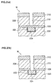
- FIG. 2(a) presents a schematic sectional view of the wafer W in the state before an SiN x layer 206 is etched.
- FIG. 2(b) presents a schematic sectional view of the wafer W in the state after the SiN x layer 206 is etched.
- the Cu layer (Cu wiring layer) 204 is formed at a first SiO 2 layer 200 via a TaN layer 202 which functions as a barrier metal layer.
- the SiN x layer 206 which is to undergo the etching process in the embodiment is formed on the Cu layer 204 to prevent the oxidization of the Cu layer 204.
- a second SiO 2 layer 208 to be used as a layer insulating film and a photoresist layer 210 having a specific pattern formed therein are sequentially laminated over the SiN x layer 206.
- the etching process is implemented in the embodiment after forming a via hole 212 which reaches the SiN x layer 206 is formed at the second SiO 2 layer 208 through a specific type of etching process as shown in FIG. 2(a).
- the processing gas introduced into the processing chamber 102 to etch the second SiO 2 layer 208 is first switched to the processing gas constituted of CH 2 F 2 , O 2 and Ar which characterizes the embodiment.
- the flow rate ratio (CH 2 F 2 /O 2 /Ar) of CH 2 F 2 , O 2 and Ar is set at, for instance, 10sccm ⁇ 30sccm / 10sccm ⁇ 30sccm / 100sccm ⁇ 200sccm.
- the pressure inside the processing chamber 102 may be set at, for instance, 30mTorr ⁇ 100mTorr. Then, high frequency power having a frequency of, for instance, 13.56 MHz and achieving a 300 W ⁇ 1000 W level is applied to the lower electrode 108.
- Such high frequency power application causes the processing gas to dissociate to generate plasma.
- the SiN x layer 206 becomes etched by the plasma and the upper surface of the Cu layer 204 becomes exposed at the bottom of the via hole 212 as shown in FIG. 2(b). Since the SiN x layer 206 has been etched by using the processing gas constituted of CH 2 F 2 , O 2 and Ar, the surface of the Cu layer 204 is hardly oxidized during this process, as explained later in reference to subsequent implementation examples.
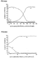
- FIGS. 3 (a) and (b) and FIGS. 4 (a) and (b) each schematically illustrate the relationship between the depth measured from the surface of the Cu layer 204 and the content of the elements present in the Cu layer 204 at the corresponding depth.
- the Cu layer 204 was gradually etched by spraying Ar at a predetermined pressure on to the exposed surface of the Cu layer 204.
- the SiN x layer 206 at the wafer W shown in the FIG. 2(a) was etched by employing the plasma processing apparatus 100 explained earlier.
- the pressure inside the processing chamber 102 was set at 50mTorr. High frequency power with a frequency set at 13.56 MHz and achieving a 500 W level was applied to the lower electrode 108.
- the results presented in FIG. 3(a) were achieved by etching the wafer under the conditions described above. As shown in FIG.
- the Cu layer 204 was hardly oxidized when the process was implemented by using the processing gas constituted of CH 2 F 2 , O 2 and Ar, with hardly any C and F injection observed. Thus, we may conclude that the processing gas is effective in preventing damage to the Cu layer 204.
- an etching process was implemented by using a processing gas constituted of CF 4 and Ar, and the results presented in FIG. 3(b) were obtained.
- the processing gas constituted of CF 4 and Ar is normally used in an etching process implemented on the SiO 2 layer 208 or the SiN X layer 206.
- an etching process was implemented by using a processing gas constituted of CH 2 F 2 , N 2 and Ar achieved by mixing N 2 instead of O 2 , in order to ascertain the extent of the influence of O 2 present in the processing gas, and the results presented in FIG. 4(a) were achieved.
- the process was implemented by setting the other processing conditions identically to those described earlier. As shown in FIG.
- the Cu layer 204 became oxidized to an even further depth and a greater degree of C/F injection was observed when the processing gas constituted of CH 2 F 2 , N 2 and Ar was used compared to the extent of the oxidation and the C/F injection observed in the process implemented by using the processing gas constituted of CH 2 F 2 , O 2 and Ar and the process implemented by using the processing gas constituted of CF 4 and Ar.
- the SiN x layer 206 covering the Cu layer 204 with the plasma generated from the processing gas constituted of CH 2 F 2 , O 2 and Ar, it is possible to minimize the extent of oxidation of the exposed Cu layer 204 and to reduce the extent to which C and F constituting the CH 2 F 2 are injected into the Cu layer 204. As a result, the electrical resistance value at the connection area does not increase even when another wiring is connected to the exposed surface of the Cu layer 204.
- the temperature of the wafer W remaining on the lower electrode 108 is sustained at 100°C or lower and preferably at 40°C.
- the temperature of the wafer W is adjusted by a temperature control mechanism (not shown) internally provided at the lower electrode 108.
- a processing gas constituted of, for instance, O 2 , is introduced into the processing chamber 102 at a flow rate of 200sccm.
- high frequency power with a frequency of 13.56 MHz and achieving a level of 1000 W is applied to the lower electrode 108.
- the processing gas is raised to plasma and thus, the photoresist layer 210 at the wafer W shown in FIG. 2(b) is removed.
- the ashing process is implemented while sustaining the temperature of the wafer W at 100°C or lower and, as a result, the degree to which the Cu layer 204 is oxidized is minimized.
- the state of the Cu layer 204 after the ashing process remains essentially unchanged from the state following the etching process.
- the processing gas introduced into the processing chamber 102 is switched to H 2 with the wafer W still remaining inside the processing chamber 102.
- the flow rate of H2 may be set at, for instance, 200sccm.
- the pressure inside the processing chamber 102 may be set at, for instance, 50mTorr.
- H 2 plasma is generated inside the processing chamber 102 by applying 1000 W high frequency power with its frequency set at, for instance, 13.56 MHz to the lower electrode 108. The H 2 plasma thus generated deoxidizes the Cu layer 204 which has been oxidized.
- the Cu layer 204 is subject to ion implant, which eliminates C and F having been injected into the Cu layer 204 during the etching process. As a result, a Cu layer 204 which does not contain O (oxygen atoms), C and F can be formed.
- the surface of the Cu layer 204 can be treated by utilizing the plasma processing apparatus 100 employed to implement the etching process and the ashing process when the method described above is adopted. This means that the surface of the Cu layer 204 does not need to be treated by employing another processing apparatus. Thus, the individual processes can be continuously performed on the plasma processing apparatus 100 to achieve an improvement in the throughput and a reduction in the production costs.
- the present invention is not limited to this example and it may be effectively implemented by using an inert gas such as He instead of Ar or without adding any inert gas.
- the present invention is not limited to this example and it may be also adopted when separate plasma processing apparatuses are employed to perform the individual processes described above.
- the SiN x layer formed on the Cu layer can be etched, while minimizing the extent to which other elements become mixed in the Cu layer.
- other elements present in the Cu layer can be eliminated through the plasma process implemented by using H 2 . As a result any degradation of the Cu layer can be prevented.
- the present invention may be adopted during the process of manufacturing semiconductor devices and, in particular, it is ideal in an application in which a plasma process such as etching is implemented on an SiN x layer formed on a Cu layer.
Landscapes
- Drying Of Semiconductors (AREA)
- Internal Circuitry In Semiconductor Integrated Circuit Devices (AREA)
- Plasma Technology (AREA)
Abstract
Description
- 100
- plasma processing apparatus
- 102
- processing chamber
- 104
- processing container
- 106
- magnet
- 108
- lower electrode
- 110
- upper electrode
- 110a
- gas outlet hole
- 112, 114, 116
- first ~ third switching valves
- 118, 120, 122
- first ~ third flow regulating valves
- 124, 126, 128
- first ~ third gas supply sources
- 130
- high frequency source
- 132
- matcher
- 134
- baffle plate
- 136
- evacuating pipe
- 200
- first SiO2 layer
- 204
- Cu layer
- 206
- SiNx layer
- 208
- second SiO2 layer
- 210
- photoresist layer
- W
- wafer
Claims (11)
- An etching method for etching an SiNx layer on a Cu layer formed at a workpiece placed inside a processing chamber by raising to plasma a processing gas introduced into said processing chamber, wherein;
said processing gas contains a gas constituted of C, H and F and O2. - An etching method according to claim 1, wherein;
said gas constituted of C, H and F is CH2F2. - An etching method according to claim 1, wherein;
said gas constituted of C, H and F is CH3F. - An etching method according to claim 1, wherein;
said gas constituted of C, H and F is CHF3. - An etching method according to claim 1, wherein;
an inert gas is added into said processing gas. - A plasma processing method comprising;
a step in which a processing gas containing a gas constituted of C, H and F and O2 is raised to plasma and an SiNx layer on a Cu layer is etched by using a photoresist layer having a specific pattern formed therein;
a step implemented after said etching step, in which said photoresist layer is ashed; and
a step implemented after said ashing step, in which H2 is introduced into said processing chamber an H2 plasma process is implemented on said Cu layer that has become exposed by raising the H2 to plasma. - An etching method according to claim 6, wherein;
said gas constituted of C, H and F is CH2F2. - An etching method according to claim 6, wherein;
said gas constituted of C, H and F is CH3F. - An etching method according to claim 6, wherein;
said gas constituted of C, H and F is CHF3. - An etching method according to claim 6, wherein;
an inert gas is added into said processing gas. - An etching method according to claim 6, wherein;
said etching step, said ashing step and said H2 etching step are implemented inside a single processing chamber.
Applications Claiming Priority (3)
| Application Number | Priority Date | Filing Date | Title |
|---|---|---|---|
| JP24142799A JP4471243B2 (en) | 1999-08-27 | 1999-08-27 | Etching method and plasma processing method |
| JP24142799 | 1999-08-27 | ||
| PCT/JP2000/005624 WO2001017007A1 (en) | 1999-08-27 | 2000-08-23 | Method of etching and method of plasma treatment |
Publications (3)
| Publication Number | Publication Date |
|---|---|
| EP1207550A1 true EP1207550A1 (en) | 2002-05-22 |
| EP1207550A4 EP1207550A4 (en) | 2002-11-06 |
| EP1207550B1 EP1207550B1 (en) | 2004-12-01 |
Family
ID=17074148
Family Applications (1)
| Application Number | Title | Priority Date | Filing Date |
|---|---|---|---|
| EP00954911A Expired - Lifetime EP1207550B1 (en) | 1999-08-27 | 2000-08-23 | Method of etching and method of plasma treatment |
Country Status (7)
| Country | Link |
|---|---|
| US (2) | US6780342B1 (en) |
| EP (1) | EP1207550B1 (en) |
| JP (1) | JP4471243B2 (en) |
| KR (1) | KR100739909B1 (en) |
| DE (1) | DE60016423T2 (en) |
| TW (1) | TW457582B (en) |
| WO (1) | WO2001017007A1 (en) |
Cited By (1)
| Publication number | Priority date | Publication date | Assignee | Title |
|---|---|---|---|---|
| WO2005104187A1 (en) * | 2004-04-02 | 2005-11-03 | Advanced Micro Devices, Inc. | In-situ surface treatment for memory cell formation |
Families Citing this family (7)
| Publication number | Priority date | Publication date | Assignee | Title |
|---|---|---|---|---|
| JP2003017469A (en) * | 2001-06-29 | 2003-01-17 | Tokyo Electron Ltd | Etching / ashing apparatus, ashing apparatus, ashing method and processing method |
| US7235884B1 (en) * | 2003-04-01 | 2007-06-26 | Altera Corporation | Local control of electrical and mechanical properties of copper interconnects to achieve stable and reliable via |
| US7101487B2 (en) * | 2003-05-02 | 2006-09-05 | Ossur Engineering, Inc. | Magnetorheological fluid compositions and prosthetic knees utilizing same |
| EP1720202A4 (en) * | 2004-02-09 | 2009-04-29 | Found Advancement Int Science | METHOD OF MANUFACTURING SEMICONDUCTOR DEVICE AND PHOTOGRAVIDE METHOD OF INSULATING FILM |
| JP2008235918A (en) * | 2008-04-16 | 2008-10-02 | Tokyo Electron Ltd | Plasma substrate processing equipment |
| CN103839604A (en) * | 2014-02-26 | 2014-06-04 | 京东方科技集团股份有限公司 | Heat conducting film, manufacturing method of heat conducting film, and array substrate |
| JP6385198B2 (en) * | 2014-08-21 | 2018-09-05 | 日東電工株式会社 | Method for manufacturing suspension board with circuit |
Family Cites Families (10)
| Publication number | Priority date | Publication date | Assignee | Title |
|---|---|---|---|---|
| JP2758754B2 (en) | 1991-12-05 | 1998-05-28 | シャープ株式会社 | Plasma etching method |
| JPH06204191A (en) * | 1992-11-10 | 1994-07-22 | Sony Corp | Surface processing method after formation of metallic plug |
| JP3390329B2 (en) | 1997-06-27 | 2003-03-24 | 日本電気株式会社 | Semiconductor device and manufacturing method thereof |
| JPH11214355A (en) | 1998-01-20 | 1999-08-06 | Nec Corp | Anisotropic dry etching method |
| US6162583A (en) * | 1998-03-20 | 2000-12-19 | Industrial Technology Research Institute | Method for making intermetal dielectrics (IMD) on semiconductor integrated circuits using low dielectric constant spin-on polymers |
| US6107208A (en) * | 1998-06-04 | 2000-08-22 | Advanced Micro Devices, Inc. | Nitride etch using N2 /Ar/CHF3 chemistry |
| US6380096B2 (en) * | 1998-07-09 | 2002-04-30 | Applied Materials, Inc. | In-situ integrated oxide etch process particularly useful for copper dual damascene |
| JP3180779B2 (en) * | 1998-10-05 | 2001-06-25 | 日本電気株式会社 | Method for manufacturing semiconductor device |
| US6093632A (en) * | 1998-12-07 | 2000-07-25 | Industrial Technology Research Institute | Modified dual damascene process |
| US6204192B1 (en) * | 1999-03-29 | 2001-03-20 | Lsi Logic Corporation | Plasma cleaning process for openings formed in at least one low dielectric constant insulation layer over copper metallization in integrated circuit structures |
-
1999
- 1999-08-27 JP JP24142799A patent/JP4471243B2/en not_active Expired - Lifetime
-
2000
- 2000-08-23 DE DE60016423T patent/DE60016423T2/en not_active Expired - Lifetime
- 2000-08-23 EP EP00954911A patent/EP1207550B1/en not_active Expired - Lifetime
- 2000-08-23 KR KR1020027002517A patent/KR100739909B1/en not_active Expired - Fee Related
- 2000-08-23 US US10/030,656 patent/US6780342B1/en not_active Expired - Lifetime
- 2000-08-23 WO PCT/JP2000/005624 patent/WO2001017007A1/en not_active Ceased
- 2000-08-25 TW TW089117250A patent/TW457582B/en not_active IP Right Cessation
-
2004
- 2004-08-02 US US10/902,893 patent/US7211197B2/en not_active Expired - Lifetime
Cited By (3)
| Publication number | Priority date | Publication date | Assignee | Title |
|---|---|---|---|---|
| WO2005104187A1 (en) * | 2004-04-02 | 2005-11-03 | Advanced Micro Devices, Inc. | In-situ surface treatment for memory cell formation |
| GB2425888A (en) * | 2004-04-02 | 2006-11-08 | Advanced Micro Devices Inc | In-situ surface treatment for memory cell formation |
| CN100470716C (en) * | 2004-04-02 | 2009-03-18 | 斯班逊有限公司 | In situ surface treatment for memory cell formation |
Also Published As
| Publication number | Publication date |
|---|---|
| JP2001068454A (en) | 2001-03-16 |
| DE60016423D1 (en) | 2005-01-05 |
| WO2001017007A1 (en) | 2001-03-08 |
| EP1207550B1 (en) | 2004-12-01 |
| TW457582B (en) | 2001-10-01 |
| US6780342B1 (en) | 2004-08-24 |
| KR100739909B1 (en) | 2007-07-16 |
| US7211197B2 (en) | 2007-05-01 |
| JP4471243B2 (en) | 2010-06-02 |
| US20050000939A1 (en) | 2005-01-06 |
| EP1207550A4 (en) | 2002-11-06 |
| DE60016423T2 (en) | 2005-11-24 |
| KR20020027588A (en) | 2002-04-13 |
Similar Documents
| Publication | Publication Date | Title |
|---|---|---|
| US4676868A (en) | Method for planarizing semiconductor substrates | |
| US7807579B2 (en) | Hydrogen ashing enhanced with water vapor and diluent gas | |
| US5176790A (en) | Process for forming a via in an integrated circuit structure by etching through an insulation layer while inhibiting sputtering of underlying metal | |
| US4547260A (en) | Process for fabricating a wiring layer of aluminum or aluminum alloy on semiconductor devices | |
| JP4825911B2 (en) | Plasma etching and photoresist strip process with defluorination and wafer defluorination steps in intervening chamber | |
| US20030207594A1 (en) | Plasma treatment of low dielectric constant dielectric material to form structures useful in formation of metal interconnects and/or filled vias for intergrated circuit structure | |
| EP0202907A2 (en) | In-situ photoresist capping process for plasma etching | |
| US6316354B1 (en) | Process for removing resist mask of integrated circuit structure which mitigates damage to underlying low dielectric constant silicon oxide dielectric layer | |
| KR20010112464A (en) | Techniques for etching a low capacitance dielectric layer | |
| JPH04239723A (en) | Manufacture of semiconductor device | |
| JPH07161703A (en) | Method for manufacturing semiconductor device | |
| US6780342B1 (en) | Method of etching and method of plasma treatment | |
| US6566269B1 (en) | Removal of post etch residuals on wafer surface | |
| US20040038541A1 (en) | Method for etching a hard mask layer and a metal layer | |
| US6472329B1 (en) | Etching aluminum over refractory metal with successive plasmas | |
| US5741742A (en) | Formation of aluminum-alloy pattern | |
| US5827436A (en) | Method for etching aluminum metal films | |
| US6740598B2 (en) | Wiring layer dry etching method and semiconductor device manufacturing method | |
| US5854137A (en) | Method for reduction of polycide residues | |
| US6492272B1 (en) | Carrier gas modification for use in plasma ashing of photoresist | |
| KR100560253B1 (en) | Plasma etching method | |
| JPH08306668A (en) | Ashing method | |
| JP2006165189A (en) | Method of manufacturing semiconductor device | |
| KR100709817B1 (en) | Etching method | |
| KR20000071322A (en) | Method of manufacturing a semiconductor device |
Legal Events
| Date | Code | Title | Description |
|---|---|---|---|
| PUAI | Public reference made under article 153(3) epc to a published international application that has entered the european phase |
Free format text: ORIGINAL CODE: 0009012 |
|
| 17P | Request for examination filed |
Effective date: 20020125 |
|
| A4 | Supplementary search report drawn up and despatched |
Effective date: 20020923 |
|
| AK | Designated contracting states |
Kind code of ref document: A4 Designated state(s): AT BE CH CY DE DK ES FI FR GB GR IE IT LI LU MC NL PT SE |
|
| 17Q | First examination report despatched |
Effective date: 20030123 |
|
| RBV | Designated contracting states (corrected) |
Designated state(s): DE FR IT |
|
| GRAP | Despatch of communication of intention to grant a patent |
Free format text: ORIGINAL CODE: EPIDOSNIGR1 |
|
| GRAS | Grant fee paid |
Free format text: ORIGINAL CODE: EPIDOSNIGR3 |
|
| GRAA | (expected) grant |
Free format text: ORIGINAL CODE: 0009210 |
|
| AK | Designated contracting states |
Kind code of ref document: B1 Designated state(s): DE FR IT |
|
| REG | Reference to a national code |
Ref country code: IE Ref legal event code: FG4D |
|
| REF | Corresponds to: |
Ref document number: 60016423 Country of ref document: DE Date of ref document: 20050105 Kind code of ref document: P |
|
| PLBE | No opposition filed within time limit |
Free format text: ORIGINAL CODE: 0009261 |
|
| STAA | Information on the status of an ep patent application or granted ep patent |
Free format text: STATUS: NO OPPOSITION FILED WITHIN TIME LIMIT |
|
| 26N | No opposition filed |
Effective date: 20050902 |
|
| ET | Fr: translation filed | ||
| PGFP | Annual fee paid to national office [announced via postgrant information from national office to epo] |
Ref country code: DE Payment date: 20130821 Year of fee payment: 14 |
|
| PGFP | Annual fee paid to national office [announced via postgrant information from national office to epo] |
Ref country code: FR Payment date: 20130808 Year of fee payment: 14 |
|
| PGFP | Annual fee paid to national office [announced via postgrant information from national office to epo] |
Ref country code: IT Payment date: 20130809 Year of fee payment: 14 |
|
| REG | Reference to a national code |
Ref country code: DE Ref legal event code: R119 Ref document number: 60016423 Country of ref document: DE |
|
| PG25 | Lapsed in a contracting state [announced via postgrant information from national office to epo] |
Ref country code: IT Free format text: LAPSE BECAUSE OF NON-PAYMENT OF DUE FEES Effective date: 20140823 |
|
| REG | Reference to a national code |
Ref country code: DE Ref legal event code: R119 Ref document number: 60016423 Country of ref document: DE Effective date: 20150303 |
|
| REG | Reference to a national code |
Ref country code: FR Ref legal event code: ST Effective date: 20150430 |
|
| PG25 | Lapsed in a contracting state [announced via postgrant information from national office to epo] |
Ref country code: DE Free format text: LAPSE BECAUSE OF NON-PAYMENT OF DUE FEES Effective date: 20150303 |
|
| PG25 | Lapsed in a contracting state [announced via postgrant information from national office to epo] |
Ref country code: FR Free format text: LAPSE BECAUSE OF NON-PAYMENT OF DUE FEES Effective date: 20140901 |