Technical Field
The present invention relates to a solid-state imaging
device for removing a background light component of
light incident on a photodetector and detecting only a
signal light component.
Background Art
A solid-state imaging device has a plurality of
photodetectors in a one- or two-dimensional array, in
which a signal current output from each photodetector
is integrated by an integration circuit, and a signal
voltage as an integration result is output. Some
solid-state imaging devices convert (A/D-convert) the
signal voltage as an analog signal into a digital
signal and output the digital signal. If the signal
voltage exceeds a predetermined value in this A/D
conversion, the digital signal that is A/D-converted
and output on the basis of the signal voltage is
saturated at a value corresponding to the predetermined
value, and consequently, accurate photodetection cannot
be performed. Conventionally, the expected maximum
value of the signal voltage or a value more than the
expected maximum value is set as the predetermined
value, thereby preventing the saturation.
Alternatively, the dynamic range is widened using a
technique such as logarithmic compression.
A solid-state imaging device is used for a
distance measuring device installed in, e.g., a camera.
In this distance measuring device, reflected light of
spot light projected from a light projecting means such
as a light-emitting diode to an object is sensed by
each of two solid-state imaging devices, and distance
measurement is executed on the basis of the two sensed
images. In sensing a spot light component (signal
light component), a background light component is also
superposed and sensed. Hence, only the background
light component is sensed by each of the two
solid-state imaging devices when no spot light is
projected, and the difference between the two images is
calculated to obtain the image of only the spot light
component, thereby improving the distance measuring
accuracy.
Disclosure of Invention
However, in the integration circuit of a
conventional solid-state imaging device, a noise error
may occur because no measures are taken against a noise
component having a value that varies at every
integration operation, such as thermal noise of an
amplifier in the integration circuit. When the
intensity of light incident on the photodetector, i.e.,
the value of the signal voltage is small, the S/N ratio
of photodetection suffers because of the noise
component that changes depending on the integration
circuit.
In A/D conversion in the conventional solid-state
imaging device, a large value is set as the
predetermined value to prevent any saturation. For
this reason, when the intensity of light incident on
the photodetector, i.e., the value of the signal
voltage is small, the resolution of the output digital
signal is poor.
As in the case wherein a solid-state imaging
device is used for a distance measuring device, when
the image of only a spot light component is to be
obtained by subtracting the image sensing result of a
background light component from the image sensing
result of the spot light component and background light
component, the following problem arises. That is, when
the background light component is larger than the spot
light component, the signal voltage obtained when the
spot light component superposed with the background
light component is incident becomes very large.
Therefore, to prevent saturation, a larger value must
be set as the predetermined value. Hence, a digital
signal output on the basis of the spot light component
obtained as a subtraction result is poorer in
resolution.
As described above, in the conventional
solid-state imaging device, the S/N ratio is low.
Additionally, in A/D conversion, the resolution of an
output digital signal is poor. The present invention
has been made to solve the above problems, and has as
its object to provide a solid-state imaging device
which has a high S/N ratio, prevents any saturation in
A/D conversion even when the incident light intensity
is high, and obtains an excellent resolution even when
the incident light intensity is low.
A solid-state imaging device according to the
present invention is characterized by comprising (1) N
(N ≧ 2) photodetectors each of which outputs a signal
current corresponding to an incident light intensity,
(2) N integration circuits each of which is arranged in
correspondence with one of the N photodetectors to
integrate charges in correspondence with a signal
current output from the photodetector and to output a
signal voltage corresponding to an amount of the
integrated charges, (3) N CDS (Correlated Double
Sampling) circuits each of which is arranged in
correspondence with one of the N integration circuits
and has a first capacitor and amplifier sequentially
inserted between an output terminal and an input
terminal for receiving the signal voltage output from
the integration circuit, second and third capacitors
having the same capacitance value and parallelly
inserted between an input and an output of the
amplifier, and switch means for selecting one of the
second and third capacitors to integrate a charge
amount corresponding to an amount of a change in signal
voltage, (4) N difference arithmetic circuits each of
which is arranged in correspondence with one of the N
CDS circuits to obtain a difference between the charge
amounts integrated in the second and third capacitors
of the CDS circuit and to output a difference signal
voltage corresponding to the difference, (5) N sample
and hold circuits (S-H circuits) each of which is
arranged in correspondence with one of the N difference
arithmetic circuits to hold and output the difference
signal voltage obtained by the difference arithmetic
circuit, (6) a reference signal voltage generation
circuit which outputs a reference signal voltage having
a monotonically increasing value, (7) N comparison
circuits each of which is arranged in correspondence
with one of the N difference arithmetic circuits to
compare a value of the difference signal voltage
obtained by the difference arithmetic circuit with the
value of the reference signal voltage output from the
reference signal voltage generation circuit and to
output a coincidence signal representing a timing when
the values coincide, (8) a final coincidence
determination circuit which receives coincidence
signals output from the N comparison circuits and
outputs a final coincidence signal representing a
latest of timings represented by the coincidence
signals, (9) a reference voltage hold circuit which
receives the final coincidence signal output from the
final coincidence determination circuit and the
reference signal voltage output from the reference
signal voltage generation circuit and holds and outputs
the value of the reference signal voltage at the timing
represented by the final coincidence signal, and (10)
an A/D conversion circuit which sets an A/D conversion
range on the basis of the value of the reference signal
voltage output from the reference voltage hold circuit,
sequentially receives the difference signal voltages
output from the N S-H circuits, converts each
difference signal voltage into a digital signal, and
outputs the digital signal.
This solid-state imaging device comprises N units
each including a photodetector, integration circuit,
CDS circuit, difference arithmetic circuit, S-H circuit,
and comparison circuit. In each unit, a signal current
corresponding to an incident light intensity is output
from the photodetector, and the integration circuit
integrates charges in correspondence with the signal
current output from the photodetector and outputs a
signal voltage corresponding to the amount of
integrated charges. In the CDS circuit, the signal
voltage output from the integration circuit is input to
the first capacitor, and one of the second and third
capacitors, which is selected by the switch means,
integrates the charge amount corresponding to the
amount of the change in input signal voltage. The
difference arithmetic circuit obtains the difference
between the charge amounts integrated in the second and
third capacitors of the CDS circuit and outputs the
difference signal voltage corresponding to the
difference. This difference signal voltage is held by
the S-H circuit. The comparison circuit compares the
value of the difference signal voltage obtained by the
difference arithmetic circuit with the value of the
reference signal voltage which is output from the
reference signal voltage generation circuit and has a
monotonically increasing value, and outputs the
coincidence signal representing the timing when the two
values coincide.
The final coincidence determination circuit
outputs the final coincidence signal representing the
latest of the timings represented by the coincidence
signals output from the N comparison circuits. The
value of the reference signal voltage at the timing
represented by the final coincidence signal is held and
output from the reference voltage hold circuit. The
held value of the reference signal voltage is the
maximum value of difference signal voltages held by the
N S-H circuits. The A/D conversion circuit sets the
A/D conversion range on the basis of the value of the
reference signal voltage output from the reference
voltage hold circuit, sequentially receives the
difference signal voltages output from the N S-H
circuits, converts each difference signal voltage into
a digital signal, and outputs the digital signal.
A solid-state imaging device according to the
present invention is also characterized in that the
solid-state imaging device further comprises a timing
control circuit which controls operations of the N
integration circuits, the N CDS circuits, the N
difference arithmetic circuits, the N S-H circuits, the
reference signal voltage generation circuit, the N
comparison circuits, the final coincidence
determination circuit, the reference voltage hold
circuit, and the A/D conversion circuit, and is used
together with light projecting means for projecting
spot light to an object, the timing control circuit
causing, (1) during a first period in which the spot
light is being projected to the object by the light
projecting means, the second capacitor of the CDS
circuit to integrate the charge amount corresponding to
the amount of the change in signal voltage output from
the integration circuit when the spot light component
and background light component become incident on the
photodetector, (2) during a second period in which the
spot light is not projected to the object by the light
projecting means, the third capacitor of the CDS
circuit to integrate the charge amount corresponding to
the amount of the change in signal voltage output from
the integration circuit when the background light
component becomes incident on the photodetector, (3)
during a third period after the first and second
periods, the difference arithmetic circuit to calculate
the difference between the charge amounts integrated in
the second and third capacitors of the CDS circuit and
to output the difference signal voltage corresponding
to the difference, and the S-H circuit to hold the
difference signal voltage, (4) during a fourth period
after the third period, the reference signal voltage
generation circuit to output the reference signal
voltage having the monotonically increasing value, the
comparison circuit to output, on the basis of
comparison between the values of the difference signal
voltage and reference signal voltage, the coincidence
signal representing the timing when the values coincide,
the final coincidence determination circuit to output
the final coincidence signal representing the latest of
the timings represented by the coincidence signals, the
reference voltage hold circuit to hold the value of the
reference signal voltage at the timing represented by
the final coincidence signal, and the A/D conversion
circuit to set the A/D conversion range on the basis of
the held value of the reference signal voltage, and (5)
during a fifth period after the fourth period, the A/D
conversion circuit to sequentially receive the
difference signal voltages output from the N S-H
circuits, convert each difference signal voltage into a
digital signal, and output the digital signal.
In this case, under the control by the timing
control circuit, during the first period, the first
charge amount corresponding to the amount of the change
in signal voltage output from the integration circuit
when the spot light component and background light
component become incident on the photodetector is
integrated in the second capacitor of the CDS circuit.
During the second period, the second charge amount
corresponding to the amount of the change in signal
voltage output from the integration circuit when the
background light component becomes incident on the
photodetector is integrated in the third capacitor of
the CDS circuit. Either the first or second period can
be set first. During the third period after the first
and second periods, the difference between the charge
amounts integrated in the second and third capacitors
of the CDS circuit is obtained by the difference
arithmetic circuit, and the difference signal voltage
corresponding to the difference is output from the
difference arithmetic circuit and held by the S-H
circuit. The difference signal voltage held by the S-H
circuit corresponds to the spot light component.
Subsequently, during the fourth period, the
reference signal voltage having the monotonically
increasing value is output from the reference signal
voltage generation circuit. On the basis of comparison
between the values of the difference signal voltage and
reference signal voltage, the comparison circuit
outputs the coincidence signal representing the timing
when the two values coincide. The final coincidence
determination circuit outputs the final coincidence
signal representing the latest of timings represented
by the coincidence signals. The reference voltage hold
circuit holds the value of the reference signal voltage
at the timing represented by the final coincidence
signal. On the basis of the held value of the
reference signal voltage, the A/D conversion range of
the A/D conversion circuit is set. During the fifth
period after the fourth period, the difference signal
voltages output from the N S-H circuits are
sequentially input to the A/D conversion circuit, each
difference signal voltage is converted into a digital
signal, and the digital signal is output from the A/D
conversion circuit.
In other words, the above solid-state imaging
device is characterized in that, in a solid-state
imaging device having an A/D conversion circuit to
which output signals from a plurality of circuit arrays
are sequentially input, each of the circuit arrays
comprises a photodetector, and a comparison circuit
which receives a signal (output signal from a
difference arithmetic circuit) corresponding to an
output from the photodetector and a monotonically
increasing voltage (output from a reference signal
voltage generation circuit), and outputs a coincidence
signal representing a timing when the signal and
voltage coincide, the solid-state imaging device
comprises a final coincidence determination circuit
which receives a plurality of coincidence signals
output from the comparison circuits and outputs a final
coincidence signal representing a latest of timings
represented by the coincidence signals, and an A/D
conversion range of the A/D conversion circuit is set
in accordance with a value of the monotonically
increasing voltage (output from the reference signal
voltage generation circuit 500) when the final
coincidence signal is output.
The final coincidence signal corresponds to a
signal for the highest incident light intensity in
signals corresponding to the outputs from the
photodetectors PD. Hence, when the A/D conversion
range is set on the basis of the final coincidence
signal, any saturation can be prevented even when the
incident light intensity is high, and an excellent
resolution can be obtained even when the incident light
intensity is low.
Brief Description of Drawings
Fig. 1 is a schematic view of the overall
arrangement of a solid-state imaging device according
to the embodiment;
Fig. 2 is a circuit diagram of the integration
circuit of the solid-state imaging device according to
the embodiment;
Fig. 3 is a circuit diagram of the CDS circuit of
the solid-state imaging device according to the
embodiment;
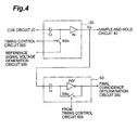
Fig. 4 is a circuit diagram of the difference
arithmetic circuit and comparison circuit of the
solid-state imaging device according to the first
embodiment;
Fig. 5 is a circuit diagram of the S-H circuit of
the solid-state imaging device according to the
embodiment;
Fig. 6 is a circuit diagram of the final
coincidence determination circuit of the solid-state
imaging device according to the embodiment;
Fig. 7 is a circuit diagram of the reference
voltage hold circuit of the solid-state imaging device
according to the embodiment;
Fig. 8 is a circuit diagram of the A/D conversion
circuit of the solid-state imaging device according to
the embodiment;
Fig. 9 is a detailed circuit diagram of the
variable capacitance integration circuit in the A/D
conversion circuit;
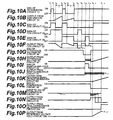
Figs. 10A, 10B, 10C, 10D, 10E, 10F, 10G, 10H, 10I,
10J, 10K, 10L, 10M, 10N, 10O, and 10P are timing charts
for explaining the operation of the solid-state imaging
device according to the embodiment;
Figs. 11A, 11B, 11C, and 11D are views for
explaining the operation of the A/D conversion circuit;
Fig. 12 is a circuit diagram of the difference
arithmetic circuit and comparison circuit of a
solid-state imaging device according to the second
embodiment;
Fig. 13 is a circuit diagram of the difference
arithmetic circuit and comparison circuit of a
solid-state imaging device according to the third
embodiment; and
Fig. 14 is a perspective view of an imaging
device having a solid-state imaging device.
Best Mode of Carrying Out the Invention
The embodiments of the present invention will be
described below in detail with reference to the
accompanying drawings. The same reference numerals
denote the same elements throughout the drawings, and a
repetitive description will be omitted. In addition, N
is an integer of 2 or more, and a suffix n is an
integer from 1 to N unless otherwise specified.
(First Embodiment)
The arrangement of a solid-state imaging device
according to the first embodiment will be described
first with reference to Figs. 1 to 9. Fig. 1 is a
schematic view of the overall arrangement of the
solid-state imaging device according to the embodiment.
The solid-state imaging device according to this
embodiment comprises N units 1001 to 100N, a final
coincidence determination circuit 200, a reference
voltage hold circuit 300, an A/D conversion circuit 400,
a reference signal voltage generation circuit 500, a
timing control circuit 600, and a shift register 700.
Each unit 100n includes a photodiode PD, an integration
circuit 10, a CDS circuit 20, a difference arithmetic
circuit 30, a S-H circuit 40, a comparison circuit 50,
and a switch SW6. The integration circuits 10 of the
units 100n have identical arrangements. The CDS
circuits 20 of the units 100n have identical
arrangements. The difference arithmetic circuits 30 of
the units 100n have identical arrangements. The S-H
circuits 40 of the units 100n have identical
arrangements. The comparison circuits 50 of the units
100n have identical arrangements. Hence, the N units
1001 to 100N have identical arrangements.
The photodiode PD of each unit 100n has an anode
terminal grounded and a cathode terminal connected to
the input terminal of the integration circuit 10. The
photodiode PD outputs a signal current corresponding to
an incident light intensity from the cathode terminal
to the input terminal of the integration circuit 10.
The photodiodes PD of the units 100n are in a one- or
two-dimensional array to image a one- or
two-dimensional object. The number of photodiodes PD
is N, and the N photodetectors form an array.
Fig. 2 is a circuit diagram of the integration
circuit 10 of the solid-state imaging device according
to the embodiment. In the integration circuit 10 of
each unit 100n, an amplifier A1, capacitor C1, and
switch SW1 are connected in parallel between the input
terminal and the output terminal. When the switch SW1
is ON, the integration circuit 10 discharges the
capacitor C1 to initialize it. On the other hand, when
the switch SW1 is OFF, the integration circuit 10
integrates charges input from the photodiode PD to the
input terminal in the capacitor C1 and outputs a signal
voltage corresponding to the integrated charges from
the output terminal. The switch SW1 is turned on/off
on the basis of a control signal output from the timing
control circuit 600.
Fig. 3 is a circuit diagram of the CDS circuit 20
of the solid-state imaging device according to the
embodiment. The CDS circuit 20 of each unit 100n has a
first capacitor C21 and amplifier A2 sequentially
between the input terminal and the output terminal. In
addition, a switch SW21, a second capacitor C22 and
switch SW22 which are serial-connected to each other,
and a third capacitor C23 and switch SW23 which are
serial-connected to each other are parallelly connected
between the input and the output of the amplifier A2.
The capacitances of the capacitors C22 and C23 are equal.
When the switches SW21 to SW23 are ON, the CDS
circuit 20 discharges the capacitors C22 and C23 to
initialize them. When the switches SW21 and SW23 are OFF,
and the switch SW22 is ON, first charges input from the
integration circuit 10 through the capacitor C21 are
integrated in the capacitor C22, and a signal voltage
corresponding to the integrated charges is output from
the output terminal. When the switches SW21 and SW22 are
OFF, and the switch SW23 is ON, second charges input
from the integration circuit 10 through the capacitor
C21 are integrated in the capacitor C23, and a signal
voltage corresponding to the integrated charges is
output from the output terminal. The switches SW21, SW22,
and SW23 are turned on/off on the basis of a control
signal output from the timing control circuit 600.
Fig. 4 is a circuit diagram of the difference
arithmetic circuit 30 and comparison circuit 50 of the
solid-state imaging device according to the first
embodiment. The difference arithmetic circuit 30 of
each unit 100n has a capacitor C3 and amplifier A3
sequentially between the input terminal and the output
terminal. The connection point between the capacitor
C3 and the amplifier A3 is connected to the reference
signal voltage generation circuit 500 through a switch
SW3. When the reference signal voltage input from the
reference signal voltage generation circuit 500 to the
switch SW3 has a predetermined potential (e.g., the
ground potential), and the switch SW3 is ON, the
difference arithmetic circuit 30 stores only charges Q1
in the capacitor C3. When the switch SW3 is OFF, the
difference arithmetic circuit 30 removes charges Q2
from the capacitor C3. With this operation, the
difference arithmetic circuit 30 integrates the
difference between the charges Q1 and Q2 input from the
CDS circuit 20, i.e., charges (Q1 - Q2) in the
capacitor C3 and outputs a difference signal voltage Vn3
corresponding to the integrated charges (Q1 - Q2) from
the amplifier A3. When the switch SW3 is ON, the
difference arithmetic circuit 30 inputs to the
amplifier A3 the reference signal voltage which is
input from the reference signal voltage generation
circuit 500 to the switch SW3 and has a monotonically
increasing value. The switch SW3 is turned on/off on
the basis of a control signal output from the timing
control circuit 600.
The comparison circuit 50 of each unit 100n has a
capacitor C5 and inverter INV sequentially between the
input terminal and the output terminal. A switch SW5
is connected between the input and the output of the
inverter INV. The switch SW5 is turned on/off on the
basis of a control signal output from the timing
control circuit 600. When the switch SW5 is ON, the
comparison circuit 50 outputs an intermediate potential
(the intermediate value between the power supply
potential and the ground potential) Vmid from the
inverter INV, and a voltage Vn1 is held on one side of
the capacitor C5. At this time, a value Vn2 of a signal
voltage output from the difference arithmetic circuit
30 is held at the terminal on the opposite side of the
capacitor C5. As a result, a charge amount obtained by
multiplying the difference potential between the
voltages values Vn1 and Vn2 by the capacitance value of
the capacitor C5 is held by the capacitor C5.
After that, when the switch SW3 of the difference
arithmetic circuit 30 is turned on, the potential Vn2 on
one side of the capacitor C5 abruptly drops to the
reference potential level at this time. Simultaneously,
when the switch SW5 of the comparison circuit 50 is
also turned off, the voltage value Vn1 also varies in
the same amount as that of the variation in voltage
value Vn2 and abruptly drops. When the reference signal
voltage from the reference signal voltage generation
circuit 500 monotonically increases, the voltage values
Vn1 and Vn2 also slowly rise in proportion to the
reference signal voltage. When the voltage value Vn1
reaches the intermediate potential Vmid, the output from
the inverter INV is abruptly inverted. With this
function, the magnitude of the output voltage value
from the difference arithmetic circuit 30 is compared
with the reference voltage. Note that the reference
signal voltage generation circuit 500 generates a saw
tooth wave having a voltage that changes as a function
of time.
As described above, the comparison circuit 50
compares the value of the reference signal voltage
output from the reference signal voltage generation
circuit 500 and received through the amplifier A3 of
the difference arithmetic circuit 30 with the voltage
value held by the capacitor C5, and outputs a logic
signal representing the comparison result. The logic
signal (coincidence signal) output from the comparison
circuit 50 is inverted at a timing when the value of
the reference signal voltage coincides the voltage
value held by the capacitor C5.
Fig. 5 is a circuit diagram of the S-H circuit 40
of the solid-state imaging device according to the
embodiment. The S-H circuit 40 of each unit 100n has a
switch SW41 and capacitor C4 sequentially between the
input terminal and the output terminal. The connection
point between the switch SW41 and the capacitor C4 is
grounded through a switch SW42, and the point between
the capacitor C4 and the output terminal is grounded
through a switch SW43. When the switches SW41 and SW43
are ON, the S-H circuit 40 stores the difference signal
voltage Vn3 output from the difference arithmetic
circuit 30 in the capacitor C4, and even after the
switch SW41 is turned off, holds the signal voltage Vn3
in the capacitor C4. The switches SW41 to SW43 are
turned on/off on the basis of a control signal output
from the timing control circuit 600. The switches SW6
of the respective units 100n are sequentially turned on
under the control of the shift register 700. When the
switches SW42 are also turned on, pieces of information
of the difference signal voltages Vn3 output from the S-H
circuits 40 are sequentially input to the A/D
conversion circuit 400 in the form of charges in
accordance with the same principle as a switched
capacitor.
Fig. 6 is a circuit diagram of the final
coincidence determination circuit 200 of the
solid-state imaging device according to the embodiment.
The final coincidence determination circuit 200 has
NMOS transistors T1 to TN and a resistor R200. The
source terminals of the respective transistors Tn are
grounded, and the drain terminals of the respective
transistors Tn are commonly connected to a power supply
voltage Vdd through the resistor R200. The gate
terminal of each transistor Tn is connected to the
output terminal of the comparison circuit 50 of a
corresponding unit 100n to receive the logic signal
output from the comparison circuit 50. In this final
coincidence determination circuit 200, the logic signal
(coincidence signal) output from the comparison circuit
50 of each unit 100n is input to the gate terminal of a
corresponding transistor Tn. When all the logic
signals change to logic L, a logic signal of logic H is
output from the output terminal to the reference
voltage hold circuit 300. The logic of the logic
signal (final coincidence signal) output from the final
coincidence determination circuit 200 is inverted at
the latest of timings when the logic of the logic
signals (coincidence signals) from the comparison
circuits 50 of the respective units 100n is inverted.
The final coincidence determination circuit 200 having
the above arrangement is preferable because the circuit
size is small. Note that the final coincidence
determination circuit 200 may be an N-input NOR logic
circuit. This circuit is preferable because an
accurate logic level value can be output, an operation
error hardly occurs, and the power consumption is low.
Fig. 7 is a circuit diagram of the reference
voltage hold circuit 300 of the solid-state imaging
device according to the embodiment. The reference
voltage hold circuit 300 has a switch SW300 and
amplifier A300 sequentially between the input terminal
and the output terminal. The connection point between
the switch SW300 and the amplifier A300 is grounded
through a capacitor C300. When the logic signal (final
coincidence signal) output from the final coincidence
determination circuit 200 changes to logic H, the
reference voltage hold circuit 300 turns off the switch
SW300 to hold in the capacitor C300 the value of the
reference signal voltage output from the reference
signal voltage generation circuit 500 at that time and
outputs the value from the amplifier A300.
Fig. 8 is a circuit diagram of the A/D conversion
circuit 400 of the solid-state imaging device according
to the embodiment. The A/D conversion circuit 400
receives the reference voltage value information output
from the reference voltage hold circuit 300 in the form
of charges and uses the reference voltage value as an
A/D conversion range. The A/D conversion circuit 400
sequentially receives the difference signal voltages Vn3
output from the S-H circuits 40 of the respective units
100n through the switches SW6, converts each signal
voltage (analog signal) into a digital signal, and
outputs the digital signal. The A/D conversion circuit
400 comprises a variable capacitance integration
circuit 410, a comparison circuit A402, a capacitance
control section 420, and a read section 430.
The variable capacitance integration circuit 410
comprises an amplifier A401, a variable capacitance
section C400, and a switch SW401. The amplifier A401
receives at its inverting input terminal a charge
amount proportional to each of the difference signal
voltages Vn3 that have been output from the S-H circuits
40 of the respective units 100 and sequentially
arrived through the switches SW6. The non-inverting
input terminal of the amplifier A401 is grounded. The
capacitance of the variable capacitance section C400 is
variable and controllable. The variable capacitance
section C400 is inserted between the inverting input
terminal and the output terminal of the amplifier A401
to integrate charges in accordance with the received
signal voltage. The switch SW401 is inserted between
the inverting input terminal and the output terminal of
the amplifier A401. When the switch SW401 is OFF, the
variable capacitance section C400 integrates charges.
When the switch SW401 is ON, charge accumulation in the
variable capacitance section C400 is reset. The
variable capacitance integration circuit 410
sequentially receives the signal voltages output from
the respective units 100n, integrates them in
accordance with the capacitance of the variable
capacitance section C400, and outputs an integration
signal as an integration result.
The comparison circuit A402 receives the
integration signal output from the variable capacitance
integration circuit 410 at its inverting input terminal
and the reference voltage value output from the
reference voltage hold circuit 300 at its non-inverting
input terminal, compares the values of the two input
signals, and outputs a comparison result signal as a
comparison result.
The capacitance control section 420 receives the
comparison result signal output from the comparison
circuit A402 and outputs a capacitance instruction
signal C which controls the capacitance of the variable
capacitance section C400 on the basis of the comparison
result signal. In addition, when it is determined on
the basis of the comparison result signal that the
value of the integration signal coincides the reference
voltage value at a predetermined resolution, the
capacitance control section 420 outputs a first digital
signal corresponding to the capacitance value of the
variable capacitance section C400.
The read section 430 receives the first digital
signal output from the capacitance control section 420
and outputs a second digital signal corresponding to
the first digital signal. The second digital signal
indicates a value obtained by removing the offset value
of the variable capacitance integration circuit 410
from the value of the first digital signal. The read
section 430 is, e.g., a memory element which receives
the first digital signal as an address and outputs data
stored at that address of the memory element as the
second digital signal. The second digital signal is
the photodetection signal output from the solid-state
imaging device according to this embodiment.
Fig. 9 is a detailed circuit diagram of the
variable capacitance integration circuit 410 in the A/D
conversion circuit 400. Fig. 9 shows a circuit
arrangement having an A/D conversion function with a
resolution of 1/24 = 1/16. A description will be done
below on the basis of this circuit arrangement.
As shown in Fig. 9, the variable capacitance
section C400 comprises capacitors C411 to C414, switches
SW411 to SW414, and switches SW421 to SW424. The capacitor
C411 and switch SW411 are serial-connected to each other
and inserted between the inverting input terminal and
the output terminal of the amplifier A401. The switch
SW421 is inserted between the ground potential and the
connection point between the capacitor C411 and the
switch SW411. The capacitor C412 and switch SW412 are
serial-connected to each other and inserted between the
inverting input terminal and the output terminal of the
amplifier A401. The switch SW422 is inserted between the
ground potential and the connection point between the
capacitor C412 and the switch SW412. The capacitor C413 and
switch SW413 are serial-connected to each other and
inserted between the inverting input terminal and the
output terminal of the amplifier A401. The switch SW423
is inserted between the ground potential and the
connection point between the capacitor C413 and the
switch SW413. The capacitor C414 and switch SW414 are
serial-connected to each other and inserted between the
inverting input terminal and the output terminal of the
amplifier A401. The switch SW424 is inserted between the
ground potential and the connection point between the
capacitor C414 and the switch SW414.
The switches SW411 to SW414 are turned on/off on the
basis of signal components C11 to C14 of the
capacitance instruction signal C output from the
capacitance control section 420, respectively. The
switches SW421 to SW424 are turned on/off on the basis of
signal components C21 to C24 of the capacitance
instruction signal C output from the capacitance
control section 420, respectively. When the
capacitance values of the capacitors C411 to C414 are
represented by C411 to C414, they satisfy
C411 = 2C412 = 4C413 = 8C414
C411 + C412 + C413 + C414 = C0
The reference signal voltage generation circuit
500 generates the reference signal voltage and supplies
it to the comparison circuit 50 of each unit 100n and
also supplies it to the reference voltage hold circuit
300. In this embodiment, the reference signal voltage
is supplied to the comparison circuit 50 indirectly
through the amplifier A3 of the difference arithmetic
circuit 30. The reference signal voltage has a
predetermined potential (e.g., the ground potential)
until the difference arithmetic circuit 30 executes the
difference arithmetic operation and the S-H circuit 40
holds the result. After that, the voltage value
monotonically increases. The shift register 700
sequentially turns on the switches SW6 of the
respective units 100n after the monotonical increase in
reference signal voltage is ended. The timing control
circuit 600 ON/OFF-controls the remaining switches and
controls the reference signal voltage output from the
reference signal voltage generation circuit 500.
The operation of the solid-state imaging device
according to this embodiment will be described next.
Figs. 10A, 10B, 10C, 10D, 10E, 10F, 10G, 10H, 10I, 10J,
10K, 10L, 10M, 10N, 10O, and 10P are timing charts for
explaining the operation of the solid-state imaging
device according to the embodiment. A case wherein the
solid-state imaging device according to this embodiment
constructs a distance measuring device together with a
light projecting means LED (Fig. 14) such as a
light-emitting diode will be described below. That is,
in the operation to be described below, a background
light component is removed, and a photodetection signal
for only a spot light component (signal light
component) projected from the light-emitting diode to
an object is output.
At time t1, the switch SW1 of the integration
circuit 10 is turned on to discharge and initialize the
capacitor C1. In addition, the switch SW21 of the CDS
circuit 20 is turned on to stop CDS operation in the
CDS circuit 20. At time t2, the switch SW1 of the
integration circuit 10 is turned off. From the time t2,
charges output from the photodiode PD are integrated in
the capacitor C1, and the signal voltage output from
the output terminal of the integration circuit 10
gradually becomes high. At this time t2, the switch
SW21 of the CDS circuit 20 remains ON. Simultaneously,
the switch SW22 is turned on to remove residual charges
from the capacitor C22. The switch SW23 is OFF. At time
t3, the switch SW21 of the CDS circuit 20 is turned off,
and the switch SW22 remains ON. At time t4 after the
elapse of a predetermined time T from the time t3, the
switch SW21 of the CDS circuit 20 is turned on, and the
switch SW22 is turned off.
During the period from the times t2 to t4, spot
light is projected from the light-emitting diode to the
object. Hence, both the spot light component and the
background light component projected from the
light-emitting diode and reflected by the object become
incident on the photodiode PD, and a signal current
generated by the components is output from the
photodiode PD. Upon receiving the signal current, the
integration circuit 10 integrates charges in the
capacitor C1 and outputs a signal voltage corresponding
to the amount of integrated charges. During the period
from the times t3 to t4 (first period), the signal
voltage output from the output terminal of the
integration circuit 10 is input to the CDS circuit 20,
charges corresponding to the amount of a change in
input signal voltage from the time t3 are integrated in
the capacitor C22, and a signal voltage corresponding to
the amount of integrated charges is output from the CDS
circuit 20. Hence, the signal voltage output from the
CDS circuit 20 at the time t4 has the voltage value Vn1
corresponding to the difference between the signal
voltages output from the integration circuit 10 at the
times t3 and t4 so that the noise component generated in
the integration circuit 10 is removed.
At the time t4, the switch SW22 is turned off, and
a charge in the capacitor C22 is held as the CDS result
at that time. Immediately after that, the switch SW1
of the integration circuit 10 is turned on to discharge
and initialize the capacitor C1. In addition, the
switch SW21 of the CDS circuit 20 is turned on to stop
CDS operation in the CDS circuit 20. Simultaneously,
the switch SW23 is turned on to remove residual charges
from the capacitor C23. At time t5, the switch SW1 of
the integration circuit 10 is turned off. From the
time t5, charges output from the photodiode PD are
integrated in the capacitor C1, and the signal voltage
output from the output terminal of the integration
circuit 10 gradually becomes high. At this time t5,
the switch SW21 of the CDS circuit 20 remains ON, and
the switch SW22 is OFF. At time t6, the switch SW21 of
the CDS circuit 20 is turned off, and the switch SW23
remains ON. At time t7 after the elapse of a
predetermined time from the time t6, the switch SW23 is
turned off, and the CDS result at that time is held by
the switch SW23 in the form of charges. After that, the
switch SW21 of the CDS circuit 20 is turned on to
prepare for the next operation.
During the period from the times t5 to t7, no spot
light is projected from the light-emitting diode to the
object. Hence, only the background light component
becomes incident on the photodiode PD, and a signal
current generated by the component is output from the
photodiode PD. Upon receiving the signal current, the
integration circuit 10 integrates charges in the
capacitor C1 and outputs a signal voltage corresponding
to the amount of integrated charges. During the period
from the times t6 to t7 (second period), the signal
voltage output from the output terminal of the
integration circuit 10 is input to the CDS circuit 20,
charges corresponding to the amount of a change in
input signal voltage from the time t6 are integrated in
the capacitor C23, and a signal voltage corresponding to
the amount of integrated charges is output from the CDS
circuit 20. Hence, the signal voltage output from the
CDS circuit 20 at the time t7 has the voltage value Vn2
corresponding to the difference between the signal
voltages output from the integration circuit 10 at the
times t6 and t7 so that the noise component generated in
the integration circuit 10 is removed.
From the time t7, the charges integrated in the
capacitor C22 of the CDS circuit 20 correspond to the
sum of the spot light component and background light
component, and the charges integrated in the capacitor
C23 of the CDS circuit 20 correspond to only the
background light component. Both the period from the
times t3 to t4 (first period) and the period from the
times t6 to t7 (second period) equal the time T. Since
the capacitance values of the capacitors C22 and C23 are
equal, the voltage value Vn1 corresponds to the sum of
the spot light component and background light component,
and the voltage value Vn2 corresponds to only the
background light component. Hence, the voltage
difference Vn3 = (Vn1 - Vn2) between them corresponds to
only the spot light component. From time t8, the
voltage difference Vn3 is obtained by the difference
arithmetic circuit 30 in the following way.
During the period from the times t7 to t11 (third
period), the switch SW1 of the integration circuit 10
is turned on to discharge the capacitor C1, and the
initialized state is maintained. The switch SW21 of the
CDS circuit 20 remains OFF. During the third period,
the difference arithmetic circuit 30 obtains the
difference between the charge amounts integrated in the
capacitors C22 and C23 of the CDS circuit 20 and outputs
a difference signal voltage corresponding to the
difference, and the S-H circuit 40 holds the difference
signal voltage output from the difference arithmetic
circuit 30.
During the period from the times t8 to t9, the
switch SW22 of the CDS circuit 20 is turned on. At this
time, the switch SW3 of the difference arithmetic
circuit 30 is ON. The signal voltage output from the
output terminal of the CDS circuit 20 during this
period has the voltage value Vn1 corresponding to the
amount of charges integrated in the capacitor C22. The
voltage value Vn1 is held by the capacitor C3 of the
difference arithmetic circuit 30.
During the period from the times t10 to t11, the
switch SW23 of the CDS circuit 20 is turned on. At this
time, the switch SW3 of the difference arithmetic
circuit 30 is OFF. The signal voltage output from the
output terminal of the CDS circuit 20 during this
period has the voltage value Vn2 corresponding to the
amount of charges integrated in the capacitor C23. At
this time, since the switch SW3 of the difference
arithmetic circuit 30 is OFF, the capacitor C3 of the
difference arithmetic circuit 30 holds the difference
Vn3 between the voltage value Vn2 and the voltage value
Vn1. The voltage value Vn3 is output through the
amplifier A3. This voltage value Vn3 corresponds to
only the spot light component.
When the switches SW41 and SW43 of the S-H circuit
40 are turned on, the voltage value Vn3 held by the
capacitor C3 of the difference arithmetic circuit 30 is
held by the capacitor C4 of the S-H circuit 40 through
the amplifier A3 of the difference arithmetic circuit
30 and the switch SW41 of the S-H circuit 40. Even
after the switch SW41 is turned off, the voltage value
Vn3 held by the capacitor C4 of the S-H circuit 40 stays
held in the form of a charge amount integrated in the
capacitor C4.
Until the time t11, the switch SW5 of the
comparison circuit 50 is ON, and the input and output
voltage levels of the inverter INV of the comparison
circuit 50 are the intermediate voltage. The value of
the difference signal voltage Vn3 obtained by the
difference arithmetic circuit 30 is held by the
capacitor C5 of the comparison circuit 50. After the
time t11, when the switch SW3 of the difference
arithmetic circuit 30 is turned on, and the switch SW5
of the comparison circuit 50 is turned off, the output
voltage level from the difference arithmetic circuit 30
drops from the voltage value Vn3 by -Vn3, and the input
voltage level of the inverter INV of the comparison
circuit 50 drops from the intermediate voltage by -Vn3
so that the signal output from the comparison circuit
50 is a logic signal of logic H.
From time t12 (fourth period), the value of the
reference signal voltage output from the reference
signal voltage generation circuit 500 monotonically
increases. In the comparison circuit 50 of each unit
100n, the voltage value Vn3 obtained by the difference
arithmetic circuit 30 and held by the capacitor C5 is
compared with the value of the reference signal voltage
output from the reference signal voltage generation
circuit 500 and received through the amplifier A3 of
the difference arithmetic circuit 30. When the two
values coincide, a logic signal (coincidence signal) of
logic L is output. The change to logic L in logic
signal output from the comparison circuit 50 indicates
the timing when the two values coincide.
When all the logic signals output from the
comparison circuits 50 of the respective units 100n
change to logic L, the final coincidence determination
circuit 200 outputs a logic signal (final coincidence
signal) of logic H. The change to logic H in logic
signal output from the final coincidence determination
circuit 200 indicates the latest of timings when the
logic signals output from the comparison circuits 50 of
the respective units 100n change to logic L. When the
logic signal output from the final coincidence
determination circuit 200 has changed to logic H, the
increase in value of the reference signal voltage
output from the reference signal voltage generation
circuit 500 may be ended.
In the reference voltage hold circuit 300, when
the logic signal output from the final coincidence
determination circuit 200 has changed to logic H, the
switch SW300 is turned off, the value of the reference
signal voltage (reference voltage value Vref) from the
reference signal voltage generation circuit 500 at that
timing is held by the capacitor C300, and even after
that, the reference voltage value Vref is output through
the amplifier A300. The reference voltage value Vref
indicates the maximum value of the difference signal
voltages Vn3 obtained by the difference arithmetic
circuits 30 of the respective units 100n and held by
the S-H circuits 40. On the basis of the reference
voltage value Vref held by the reference voltage hold
circuit 300, the A/D conversion range of the A/D
conversion circuit 400 is set.
During the period after the A/D conversion range
of the A/D conversion circuit 400 is set (fifth period),
the switches SW6 of the respective units 100n are
sequentially turned on by the shift register 700. When
the switch SW401 is temporarily turned on to remove all
charges from the variable capacitance section C400 to
reset it, the switch SW401 is turned off, and then the
switches SW6 and switches SW42 are simultaneously turned
off, charge amounts proportional to the difference
signal voltages Vn3 output from the S-H circuits 40 of
the respective units 100n are transferred to the
variable capacitance section C400. In this way,
voltages corresponding to the difference signal
voltages Vn3 are sequentially input to the variable
capacitance section C400 of the A/D conversion circuit
400 in the form of charges and converted into digital
signals. The digital signals are output from the A/D
conversion circuit 400.
The operation of the A/D conversion circuit 400
will be described next with reference to Figs. 11A, 11B,
11C, and 11D. At time t13, the switch SW401 of the
variable capacitance integration circuit 410 is ON, so
that the variable capacitance integration circuit 410
is in the reset state. The switches SW411 to SW414 of the
variable capacitance integration circuit 410 are ON,
the switches SW421 to SW424 are OFF, and the capacitance
value of the variable capacitance section C400 is set to
C0.
At certain time from the time t13, the switch SW401
of the A/D conversion circuit 400 is turned off, and
the switch SW6 of the first unit 1001 is turned on.
When the switches SW41 and SW43 are turned off, and the
switch SW42 is turned on, a charge amount Q integrated
in the capacitor C4 of the S-H circuit 40 of the unit
1001 is input to the variable capacitance integration
circuit 410 of the A/D conversion circuit 400 through
the switch SW6. When the charge amount Q is input to
the variable capacitance integration circuit 410, the
charges Q corresponding to the value of a signal
voltage V13 and the capacitance value C0 of the variable
capacitance section C400 flow into the variable
capacitance section C400 (Fig. 11A). At this time, a
value Vsa of the integration signal output from the
variable capacitance integration circuit 410 is given
by
Vsa = V13 = Q/C0
Subsequently, the capacitance control section 420
turns off the switches SW412 to SW414 of the variable
capacitance section C400 and then turns on the switches
SW422 to SW424 (Fig. 11B). As a consequence, the
capacitance value of the variable capacitance section
C400 becomes C411, and a value Vsb of the integration
signal output from the variable capacitance integration
circuit 410 is given by
Vsb = Q/C411
This integration signal is input to the comparison
circuit A402, and its value is compared with the
reference voltage value Vref.
If Vsb > Vref, upon receiving the comparison result,
the capacitance control section 420 also turns off the
switch SW422 of the variable capacitance section C400 and
then turns on the switch SW412 (Fig. 11C). As a result,
the capacitance value of the variable capacitance
section C400 becomes C411 + C412, and a value Vsc of the
integration signal output from the variable capacitance
integration circuit 410 is given by
Vsc = Q/(C411 + C412)
This integration signal is input to the comparison
circuit A402, and its value is compared with the
reference voltage value Vref.
If Vsb < Vref, upon receiving the comparison result,
the capacitance control section 420 also turns off the
switches SW411 and SW422 of the variable capacitance
section C400 and then turns on the switches SW412 and SW421
(Fig. 11D). As a result, the capacitance value of the
variable capacitance section C400 becomes C412, and a
value Vsd of the integration signal output from the
variable capacitance integration circuit 410 is given
by
Vsd = Q/C412
This integration signal is input to the comparison
circuit A402, and its value is compared with the
reference voltage value Vref.
In a similar way, until the capacitance control
section 420 determines that the value of the
integration signal is equal to the reference potential
Vref at a predetermined resolution, the feedback loop
formed from the variable capacitance integration
circuit 410, comparison circuit A402, and capacitance
control section 420 repeatedly sets the capacitance
value of the variable capacitance section C400 and
compares the value of the integration signal with the
reference voltage value Vref. When capacitance control
for all the capacitors C411 to C414 of the variable
capacitance section C400 is ended, the capacitance
control section 420 outputs a digital signal
corresponding to the final capacitance value of the
variable capacitance section C400 to the read section
430.
The read section 430 receives the digital signal
output from the capacitance control section 420 as an
address and outputs digital data stored at the address
of the memory as a photodetection signal of the
solid-state imaging device according to this embodiment.
In the above-described way, the signal voltage V13
corresponding to the spot light intensity incident on
the photodiode PD of the first unit 1001 is converted
into a digital signal by the A/D conversion circuit 400,
and the digital signal is output as a photodetection
signal. In a similar manner, the difference signal
voltages Vn3 corresponding to the spot light intensity
incident on the photodiodes PD of the second and
subsequent units 100n are converted into digital
signals, and the digital signals are sequentially
output as photodetection signals.
The maximum value of the signal voltages Vn3 input
to the variable capacitance integration circuit 410 is
the reference voltage value Vref, and the maximum value
of the capacitance values of the variable capacitance
section C400 is C0. Hence, the maximum value of the
amount of charges Q flowing into the variable
capacitance section C400 is obtained as Vref ↕ C0 from
equation (3). When the nth signal voltage Vn3 has the
reference voltage value Vref, all the switches SW411 to
SW414 of the variable capacitance section C400 are turned
on, and the capacitance value of the variable
capacitance section C400 becomes C0. On the other hand,
when another nth signal voltage Vn3 has a value smaller
than the reference voltage value Vref, the amount of
charges Q flowing into the variable capacitance section
C400 is smaller than Vref ↕ C0. For this reason, when any
one of the switches SW411 to SW414 of the variable
capacitance section C400 is turned off, the integration
signal output from the variable capacitance integration
circuit 410 equals the reference voltage value Vref.
As described above, the reference voltage value
Vref output from the reference voltage hold circuit 300
and input to the comparison circuit A402 defines the
maximum value of the difference signal voltages Vn3 that
can be A/D-converted by the A/D conversion circuit 400
without causing any saturation, i.e., the A/D
conversion range. In addition, since one of the signal
voltages Vn3 input to the A/D conversion circuit 400
always has the reference voltage value Vref, the entire
A/D conversion range can be effectively utilized. That
is, the solid-state imaging device according to this
embodiment is not saturated even when the incident
light intensity is high and obtains an excellent
resolution for A/D conversion even when the incident
light intensity is low.
In addition, even when the image of only a spot
light component is to be obtained by subtracting the
image sensing result of a background light component
from the image sensing result of the spot light
component and background light component, like a case
wherein the solid-state imaging device is used for a
distance measuring device, and the background light
component of the light incident on the photodiode PD is
larger than the spot light component, the digital
signal output from the A/D conversion circuit 400 on
the basis of the spot light component obtained as the
subtraction result has an excellent resolution.
Furthermore, in this embodiment, when both the
spot light component and the background light component
are incident on the photodiode PD, the variation amount
Vn1 in signal voltage output from the integration
circuit 10 during the predetermined period T is held by
the capacitor C22 of the CDS circuit 20. When only the
background light component is incident on the
photodiode PD, the variation amount Vn2 in signal
voltage output from the integration circuit 10 during
the predetermined period T is held by the capacitor C23
of the CDS circuit 20. After that, the difference
signal voltage Vn3 corresponding to the difference
between the voltage value Vn1 and the voltage value Vn2
is obtained by the difference arithmetic circuit 30 and
output from the S-H circuit 40. Hence, a noise
component generated in the integration circuit 10 is
removed from the voltage value Vn1 or Vn2 output for the
CDS circuit 20 or the difference signal voltage Vn3
output from the S-H circuit 40.
(Second Embodiment)
The arrangement of a solid-state imaging device
according to the second embodiment will be described
next. The solid-state imaging device according to the
second embodiment is different from the first
embodiment in the circuit arrangements of a difference
arithmetic circuit 30 and comparison circuit 50.
Fig. 12 is a circuit diagram of the difference
arithmetic circuit 30 and comparison circuit 50 of the
solid-state imaging device according to the second
embodiment.
The difference arithmetic circuit 30 of each unit
100n has a capacitor C3 and amplifier A3 sequentially
between the input terminal and the output terminal.
The connection point between the capacitor C3 and the
amplifier A3 is grounded through a switch SW3. When the
switch SW3 is ON, the difference arithmetic circuit 30
stores only charges Q1 in the capacitor C3. When the
switch SW3 is OFF, the difference arithmetic circuit 30
removes charges Q2 from the capacitor C3. With this
operation, the difference arithmetic circuit 30 holds
the difference between the charges Q1 and Q2 input from
a CDS circuit 20, i.e., charges (Q1 - Q2) in the
capacitor C3 and outputs a signal voltage corresponding
to the held charges (Q1 - Q2) from the amplifier A3.
The switch SW3 is turned on/off on the basis of a
control signal output from a timing control circuit 600.
The comparison circuit 50 of each unit 100n has
two input terminals and one output terminal. The
comparison circuit 50 has a switch SW52 (SW53), capacitor
C5, and inverter INV sequentially between the first
(second) input terminal and the output terminal. A
switch SW51 is connected between the input and the
output of the inverter INV. The switches SW51 to SW53
are turned on/off on the basis of a control signal
output from the timing control circuit 600.
During the third period in which the difference
between the charge amounts held in capacitors C22 and C23
of the CDS circuit 20 is obtained by the difference
arithmetic circuit 30 and held by a S-H circuit 40, the
comparison circuit 50 turns on the switch SW51 to output
the intermediate potential from the inverter INV and
also turns on the switch SW52 and off the switch SW53 to
hold a voltage value Vn3 output from the difference
arithmetic circuit 30 by the capacitor C3. During the
fourth period following the third period, the
comparison circuit 50 turns off the switches SW51 and
SW52 and turns on the switch SW53 to compare the value of
the reference signal voltage output from a reference
signal voltage generation circuit 500 with the voltage
value Vn3 held by the capacitor C5 and outputs a logic
signal representing the comparison result. The logic
of the logic signal output from the comparison circuit
50 is inverted at a timing when the value of the
reference signal voltage coincides the voltage value Vn3
held by the capacitor C5.
The operation and effect of the solid-state
imaging device according to this embodiment are the
same as in the first embodiment.
(Third Embodiment)
The arrangement of a solid-state imaging device
according to the third embodiment will be described
next. The solid-state imaging device according to the
third embodiment is different from the second
embodiment in the circuit arrangement of a comparison
circuit 50. Fig. 13 is a circuit diagram of a
difference arithmetic circuit 30 and comparison circuit
50 of the solid-state imaging device according to the
third embodiment.
The comparison circuit 50 of each unit 100n has
two input terminals and one output terminal, and also,
a switch SW5, capacitor C5, and differential comparator
COMP. The non-inverting input terminal of the
differential comparator COMP is grounded through the
capacitor C5 and also connected, through the switch SW5,
to the first input terminal which receives the signal
voltage output from the difference arithmetic circuit
30. The inverting input terminal of the differential
comparator COMP is connected to the second input
terminal which receives the reference signal voltage
output from a reference signal voltage generation
circuit 500. The switch SW5 is turned on/off on the
basis of a control signal output from a timing control
circuit 600.
During the third period in which the difference
between the charge amounts integrated in capacitors C22
and C23 of a CDS circuit 20 is obtained by the
difference arithmetic circuit 30 and held by a S-H
circuit 40, the comparison circuit 50 turns on the
switch SW5 to hold a voltage value Vn3 output from the
difference arithmetic circuit 30 by a capacitor C3.
During the fourth period following the third period,
the comparison circuit 50 turns off the switch SW5 to
compare, by the differential comparator COMP, the value
of the reference signal voltage output from the
reference signal voltage generation circuit 500 with
the voltage value Vn3 held by the capacitor C5 and
outputs a logic signal representing the comparison
result. The logic of the logic signal output from the
comparison circuit 50 is inverted at a timing when the
value of the reference signal voltage coincides the
voltage value Vn3 held by the capacitor C5.
The operation and effect of the solid-state
imaging device according to this embodiment are the
same as in the first embodiment. Especially, in this
embodiment, since comparison is done by the
differential comparator COMP without depending on any
capacitor input, the influence of a parasitic
capacitance is small, and the comparison accuracy is
high.
Fig. 14 is a perspective view of a distance
measuring device in which an imaging device having the
above-described solid-state imaging device is mounted.
The solid-state imaging device shown in Fig. 1 is
formed from a semiconductor chip SC. In this imaging
device, the semiconductor chip SC is accommodated in a
package PKG made of a ceramic. An A/D conversion
circuit 400 can be either formed in the semiconductor
chip SC or connected to the outside of the
semiconductor chip SC. When the semiconductor chip SC
includes the A/D conversion circuit 400, output
terminals TM of the A/D conversion circuit 400 are
prepared on a side surface of the package PKG.
Otherwise, the output terminals TM to output signals to
be input to the A/D conversion circuit 400 are prepared.
The package PKG has a concave portion, and the
semiconductor chip SC is arranged in the concave
portion. A step portion STEP is formed in the inner
surface of the concave portion. A filter F is arranged
on the step portion STEP. The concave portion of the
package PKG is closed by the filter F. The gap between
the filter F and the package PKG is filled with an
adhesive AHV. The filter F is an infrared filter which
selectively transmits infrared rays and is made of Si.
Note that the semiconductor chip SC is also made of Si.
Infrared rays transmitted through the filter F
become incident on the array of photodiodes PD arranged
on the surface of the semiconductor chip SC. An image
signal corresponding to the incident image is output
from the output terminal TM.
This imaging device is mounted on a circuit board
CB. That is, a socket SKT is fixed on the circuit
board CB, and the imaging device is fitted into the
socket SKT such that the terminals TM come into contact
with the inner surface of the socket SKT. A light
source LED is also arranged on the circuit board CB.
That is, this device has the light source LED which
supplies light to be incident on the solid-state image
sensing element SC, and the solid-state imaging device
SC and light source LED are fixed on the single circuit
board CB.
When the incident image is a light spot from the
infrared light source LED arranged at the fixed
position, the light spot incident position can be
detected on the basis of the image signal. That is,
the light source LED emits infrared rays to the object,
reflected light from the object is focused by a lens LS
to form a light spot on the semiconductor chip SC, the
distance (incident position) of the light spot from the
reference position is obtained on the basis of the
image signal, and the distance to the object is
calculated on the basis of the incident position. Note
that the lens LS is fixed with respect to the circuit
board CB.
For this arithmetic processing, the principle of
triangulation can be used. That is, since the incident
position of the light spot changes depending on the
distance between the light source LED and the
semiconductor chip SC, this device can be used for a
distance measuring device. This arithmetic processing
is executed by a digital processor mounted on the
circuit board CB.
As has been described above in detail, according
to the present invention, in each of the N units, a
signal current corresponding to an incident light
intensity is output from the photodetector, and the
integration circuit integrates charges in accordance
with the signal current output from the photodetector
and outputs a signal voltage corresponding to the
amount of the integrated charges. In the CDS circuit,
the signal voltage output from the integration circuit
is input to the first capacitor, and a charge amount
corresponding to the amount of a change in input signal
voltage is integrated in one of the second and third
capacitors, which is selected by a switch means. The
difference arithmetic circuit obtains the difference
between the charge amounts integrated in the second and
third capacitors of the CDS circuit and outputs a
difference signal voltage corresponding to the
difference. This difference signal voltage is held by
the S-H circuit. The comparison circuit compares the
value of the difference signal voltage obtained by the
difference arithmetic circuit with the value of the
reference signal voltage which is output from the
reference signal voltage generation circuit and has a
monotonically increasing value, and outputs a
coincidence signal representing a timing when the two
values coincide.
In addition, according to the present invention,
the final coincidence determination circuit outputs a
final coincidence signal representing the latest of
timings represented by coincidence signals output from
the N comparison circuits. The reference voltage hold
circuit holds and outputs the value of the reference
signal voltage at the timing indicated by the final
coincidence signal. The held value of the reference
signal voltage is the maximum value of difference
signal voltages held by the N S-H circuits. The A/D
conversion circuit sets the A/D conversion range on the
basis of the value of the reference signal voltage
output from the reference voltage hold circuit,
sequentially receives the difference signal voltages
output from the N S-H circuits, converts each
difference signal voltage into a digital signal, and
outputs the digital signal.
Hence, even when the integration circuit has a
noise variation that varies at every integration
operation, the CDS circuit cancels the noise error.
Even when the incident light intensity is high, no
saturation occurs, and even when the incident light
intensity is low, the resolution is excellent.
During the first period, charges corresponding to
the spot light component (signal light component) and
background light component are integrated in one of the
second and third capacitors of the CDS circuit. During
the second period, charges corresponding to the
background light component are integrated in the other
capacitor. During the third period, the difference
(signal light component) between the charge amounts is
obtained by the difference arithmetic circuit and held
by the S-H circuit. Subsequently, during the fourth
period, the reference signal voltage having a
monotonically increasing value is output from the
reference signal voltage generation circuit. On the
basis of comparison between the values of the
difference signal voltage and reference signal voltage,
the comparison circuit outputs a coincidence signal
representing a timing when the two values coincide.
The final coincidence determination circuit outputs a
final coincidence signal representing the latest of
timings represented by coincidence signals. The
reference voltage hold circuit holds the value of the
reference signal voltage at the timing represented by
the final coincidence signal. On. the basis of the held
value of the reference signal voltage, the A/D
conversion range of the A/D conversion circuit is set.
During the fifth period, difference signal voltages
output from the N S-H circuits are sequentially input
to the A/D conversion circuit, each difference signal
voltage is converted into a digital signal, and the
digital signal is output from the A/D conversion
circuit. With this arrangement, the background light
component is removed, and the S/N ratio of
photodetection for a signal light component becomes
high.
For the above solid-state imaging device, a
solid-state imaging device having an A/D conversion
circuit 400 to which output signals from a plurality of
circuit arrays (PD, 10, 20, 30, 50, 40, and SW6) are
sequentially input is characterized in that each of the
circuit arrays comprises a photodetector PD, and a
comparison circuit 50 which receives a signal (output
signal from a difference arithmetic circuit 30)
corresponding to an output from the photodetector PD
and a monotonically increasing voltage (output from a
reference signal voltage generation circuit 500), and
outputs a coincidence signal representing a timing when
the signal and voltage coincide, the solid-state
imaging device comprises a final coincidence
determination circuit 200 which receives a plurality of
coincidence signals output from the comparison circuits
50 and outputs a final coincidence signal representing
the latest of timings represented by the coincidence
signals, and the A/D conversion range of the A/D
conversion circuit 400 is set in accordance with the
value of the monotonically increasing voltage (output
from the reference signal voltage generation circuit
500) when the final coincidence signal is output.
The final coincidence signal corresponds to a
signal for the highest incident light intensity (light
intensity) in signals corresponding to the outputs from
the photodetectors PD. Hence, when the A/D conversion
range is set on the basis of the final coincidence
signal, any saturation can be prevented even when the
incident light intensity is high, and an excellent
resolution can be obtained even when the incident light
intensity is low.
Industrial Applicability
The present invention can be used for a
solid-state imaging device and distance measuring
device.