EP1203651A1 - Optical sheet - Google Patents
Optical sheet Download PDFInfo
- Publication number
- EP1203651A1 EP1203651A1 EP00935644A EP00935644A EP1203651A1 EP 1203651 A1 EP1203651 A1 EP 1203651A1 EP 00935644 A EP00935644 A EP 00935644A EP 00935644 A EP00935644 A EP 00935644A EP 1203651 A1 EP1203651 A1 EP 1203651A1
- Authority
- EP
- European Patent Office
- Prior art keywords
- optical sheet
- stress
- metal mold
- sheet
- fresnel lens
- Prior art date
- Legal status (The legal status is an assumption and is not a legal conclusion. Google has not performed a legal analysis and makes no representation as to the accuracy of the status listed.)
- Granted
Links
Images


Classifications
-
- G—PHYSICS
- G02—OPTICS
- G02B—OPTICAL ELEMENTS, SYSTEMS OR APPARATUS
- G02B3/00—Simple or compound lenses
- G02B3/0006—Arrays
- G02B3/0012—Arrays characterised by the manufacturing method
- G02B3/0031—Replication or moulding, e.g. hot embossing, UV-casting, injection moulding
-
- G—PHYSICS
- G02—OPTICS
- G02B—OPTICAL ELEMENTS, SYSTEMS OR APPARATUS
- G02B3/00—Simple or compound lenses
-
- B—PERFORMING OPERATIONS; TRANSPORTING
- B29—WORKING OF PLASTICS; WORKING OF SUBSTANCES IN A PLASTIC STATE IN GENERAL
- B29C—SHAPING OR JOINING OF PLASTICS; SHAPING OF MATERIAL IN A PLASTIC STATE, NOT OTHERWISE PROVIDED FOR; AFTER-TREATMENT OF THE SHAPED PRODUCTS, e.g. REPAIRING
- B29C37/00—Component parts, details, accessories or auxiliary operations, not covered by group B29C33/00 or B29C35/00
- B29C37/005—Compensating volume or shape change during moulding, in general
-
- G—PHYSICS
- G02—OPTICS
- G02B—OPTICAL ELEMENTS, SYSTEMS OR APPARATUS
- G02B3/00—Simple or compound lenses
- G02B3/0006—Arrays
- G02B3/0012—Arrays characterised by the manufacturing method
- G02B3/0025—Machining, e.g. grinding, polishing, diamond turning, manufacturing of mould parts
-
- G—PHYSICS
- G02—OPTICS
- G02B—OPTICAL ELEMENTS, SYSTEMS OR APPARATUS
- G02B3/00—Simple or compound lenses
- G02B3/02—Simple or compound lenses with non-spherical faces
- G02B3/06—Simple or compound lenses with non-spherical faces with cylindrical or toric faces
-
- G—PHYSICS
- G02—OPTICS
- G02B—OPTICAL ELEMENTS, SYSTEMS OR APPARATUS
- G02B3/00—Simple or compound lenses
- G02B3/02—Simple or compound lenses with non-spherical faces
- G02B3/08—Simple or compound lenses with non-spherical faces with discontinuous faces, e.g. Fresnel lens
-
- G—PHYSICS
- G03—PHOTOGRAPHY; CINEMATOGRAPHY; ANALOGOUS TECHNIQUES USING WAVES OTHER THAN OPTICAL WAVES; ELECTROGRAPHY; HOLOGRAPHY
- G03B—APPARATUS OR ARRANGEMENTS FOR TAKING PHOTOGRAPHS OR FOR PROJECTING OR VIEWING THEM; APPARATUS OR ARRANGEMENTS EMPLOYING ANALOGOUS TECHNIQUES USING WAVES OTHER THAN OPTICAL WAVES; ACCESSORIES THEREFOR
- G03B21/00—Projectors or projection-type viewers; Accessories therefor
- G03B21/54—Accessories
- G03B21/56—Projection screens
- G03B21/60—Projection screens characterised by the nature of the surface
- G03B21/62—Translucent screens
- G03B21/625—Lenticular translucent screens
-
- B—PERFORMING OPERATIONS; TRANSPORTING
- B29—WORKING OF PLASTICS; WORKING OF SUBSTANCES IN A PLASTIC STATE IN GENERAL
- B29L—INDEXING SCHEME ASSOCIATED WITH SUBCLASS B29C, RELATING TO PARTICULAR ARTICLES
- B29L2011/00—Optical elements, e.g. lenses, prisms
-
- B—PERFORMING OPERATIONS; TRANSPORTING
- B29—WORKING OF PLASTICS; WORKING OF SUBSTANCES IN A PLASTIC STATE IN GENERAL
- B29L—INDEXING SCHEME ASSOCIATED WITH SUBCLASS B29C, RELATING TO PARTICULAR ARTICLES
- B29L2011/00—Optical elements, e.g. lenses, prisms
- B29L2011/0016—Lenses
- B29L2011/005—Fresnel lenses
Definitions
- the present invention relates to an optical sheet having very fine surface irregularities such as a Fresnel lens sheet or a lenticular lens sheet to be used for a screen of a projection TV or a projector, or a condensing Fresnel lens sheet or an emboss sheet.
- a large size lens sheet such as Fresnel lens sheet, lenticular lens sheet, etc.
- a press method According to this method, a planar lenticular mold having irregular surface pattern to match the irregular surface pattern of the desired lens surface is heated, and by pressing this lenticular mold onto a resin plate, irregular surface pattern on the surface of the lenticular mold is transferred to the resin plate.
- this press method has such problems that molding cycle is long and productivity is not very high.
- a photo-polymer method (2P method) has been recently developed. According to this method, UV-setting resin is coated on a lenticular mold, and a resin plate is placed on it. Then, ultraviolet ray is irradiated to harden the UV-setting resin, and a large size lens sheet is formed.
- the productivity is not sufficiently improved by the use of this 2P method.
- a metal mold having irregular surface pattern to match the irregular surface pattern of the desired lens is used, and a relatively small size optical sheet is molded by an injection molding method.
- molten resin is injected and filled in a cavity of the metal mold, and pressure is applied in the cavity via the molten resin in spool or runner until gate is cooled down and solidified (dwell pressure application process), and the pattern of the metal mold is transferred to the resin. After the gate is solidified, the resin in the metal mold is cooled down and solidified, and a molded product (optical sheet) is obtained.
- the molten resin injected and filled in the cavity by the injection molding method is quickly cooled down when it is brought into contact with the surface of the cavity.
- a cooled and solidified layer is formed, and the molten resin is filled in the cavity.
- pressure distribution occurs in the cavity as the molten resin is filled. This exerts action as residual stress of the molded product and causes warping, deformation, etc. after molding. Dwell pressure is applied to compensate shrinkage of the molded product after injection molding, and this also causes residual stress in the molded product.
- an object of the present invention to provide an optical sheet, which has lower residual stress and is free from warping, deformation, etc.
- the optical sheet according to the present invention is an optical sheet produced by injection molding method and having stress of up to 200 kg/cm 2 on surfaces of two opposing main planes.
- each of stresses on the surfaces of the two opposing main planes is preferably up to 200 kg/cm 2
- difference of stress on the two main planes is preferably within 20%.
- main planes means two opposing planes having large area and corresponding to exit surface of the light and to rear surface of the optical sheet.
- this optical sheet has an area or 4000 cm 2 or more and thickness of 4 mm or less.
- an optical sheet is produced by an injection molding method
- one of the following methods is used to limit stress on the surface of the optical sheet up to 200 kg/cm 2 :
- An ordinary injection method an injection molding method under low pressure molding by reducing filling pressure, or an injection compression molding method.
- annealing post-processing should be performed so that the stress on the surface will be up to 200 kg/cm 2 .
- the optical sheet prepared by the injection compression molding method is sandwiched between glass plates.
- annealing is performed for 2 - 4 hours at an environmental temperature, which is by 10 °C to 20 °C lower than deflection temperature under load (to be determined by the method such as ASTM D648) of a molding material, which constitutes the optical sheet.
- the injection molding method (proposed in JP-A-11-129305) is used, it is possible to limit the stress on the surface of the optical sheet to 200 kg/cm 2 or less without performing annealing procedure, depending on the preset molding condition.
- a thin plate member such as nickel plate having a low thermal conductivity member (such as polyimide film) attached on its rear surface is placed in a cavity of a metal mold, and a molding material is filled in the metal mold. Near the surface of the metal mold where temperature is decreased from a level of transfer initiation temperature or higher to a level lower than the transfer initiation temperature, the molding material is cooled down through the contact with the metal mold.
- the low thermal conductivity member is designed to have such thickness that temperature of the molding material is again increased to the level higher than the transfer initiation temperature.
- cavity volume of the metal mold is changed during injection and filling or after the completion of the filling of the synthetic resin. (Cavity volume is increased and then decreased, or it is decreased after increased.)
- thermoplastic resin used in the injection molding so far as it is a transparent thermoplastic resin.
- synthetic resin used in the injection molding so far as it is a transparent thermoplastic resin.
- polymethyl methacrylate, polycarbonate, polystyrene, thermoplastic elastomer, non-crystalline polyolefin, polyamide, or copolymer of these substances may be used.
- This has a cavity of planar shape in size of 200 ⁇ 220 ⁇ 4.0 mm (length ⁇ width ⁇ thickness).
- a Fresnel lens pattern of 10 to 80 ⁇ m in height is formed on one of the main planes.
- a gate of 25 mm in width and 3.5 mm in thickness is provided at the center of lateral side of the metal mold. Gate of the lens sheet (optical sheet) is cut using heat nipper or saw blade.
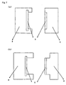
- the configuration of the metal mold No. 1 is as shown in Fig. 7 (a).
- Thin plate members 5 are mounted on a movable side 3 and a fixed side 4, and the Fresnel lens pattern is formed on one of the thin plate members 5. When necessary, the member with low thermal conductivity is attached on rear surface of the thin plate member.
- This has a cavity of planar shape in size of 400 ⁇ 800 ⁇ 4.0 mm (length ⁇ width ⁇ thickness).
- a Fresnel lens pattern of 10 to 80 ⁇ m in height is formed on one of the main planes.
- a gate in size of 25 mm in width and 3.5 mm in thickness is provided at the center of lateral side of the metal mold.
- the configuration of the metal mold No. 2 is as shown in Fig. 7 (b).
- Thin plate members 5 are mounted on a moving side 3 and a fixed side 4 respectively, and the Fresnel lens pattern is formed on one of the thin plate members 5.
- the member with low thermal conductivity is attached on rear surface of the thin plate member.
- the metal molds No. 3 to No. 5 have the same arrangement as the metal mold No. 2.
- This has a cavity of planar shape in size of 500 ⁇ 900 ⁇ 2.0 mm (length ⁇ width ⁇ thickness).
- a Fresnel lens pattern of 10 to 80 ⁇ m in height is formed on one of the main planes.
- a gate of 25 mm in width and 1.5 mm in thickness is provided at the center of lateral side of the metal mold.
- This has a cavity of planar shape in size of 700 ⁇ 900 ⁇ 2.0 mm (length ⁇ width ⁇ thickness).
- a Fresnel lens pattern of 10 to 80 ⁇ m in height is formed on one of the main planes.
- a prism pattern of 10 ⁇ m in height is formed on the other surface.
- a gate of 500 mm in width and 1.5 mm in thickness is provided at the center of lateral side of this metal mold.
- This has a cavity of planar shape in size of 800 ⁇ 1000 ⁇ 2.0 mm (length ⁇ width ⁇ thickness).
- a Fresnel lens pattern of 10 to 80 ⁇ m in height is formed.
- a prism pattern of 10 ⁇ m in height is formed.
- a gate of 500 mm in width and 1.5 mm in thickness is provided at the center of lateral side of this metal mold.
- a methacrylic resin molding material "Parapet GH-1000S" (trade name; product by Kuraray Co., Ltd.) was used.
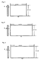
- the deformation amount of the optical sheet 1 was measured at each of the corners of the molded product. Specifically, the optical sheet 1 was placed on a platen 2, and a gap L between the platen 2 and the optical sheet 1 was measured using a thickness gauge, and a error between the form of the metal mold and the form of the optical sheet was determined.
- Reliability test of the optical sheet was performed using a constant temperature and humidity chamber (manufactured by Tabai Co., Ltd.). Testing condition was 50 °C at 80% relative humidity for 300 hours.
- optical sheets were prepared under the molding condition and the annealing condition shown in Table 1.
- injecting condition and cooling time were the same.
- the injecting condition was 100 cc/sec., and the cooling time was 60 sec.
- stress on the surface layer where the Fresnel lens pattern was formed was measured by the measuring method of (d) above.
- each optical sheet was left to stand under environmental condition of 50 °C and 80% relative humidity in the constant temperature and humidity chamber as given in (g) above.
- the amount of deformation after 300 hours was determined by the measuring method given in (f) above. The results are summarized in Table 2 and Table 3.
- measuring position of the stress and the deformation shown in Tables 2 and 3 were as follows : Measuring positions A - D were at four corners of the lens sheet, and the measuring position E is at the center. (The same applies to Table 5 as given later.) Molding machine Resin temperature (°C) and metal mold temperature (°C) Metal mold (Thin plate member (thickness in mm) /low thermal conductivity member (thickness in mm) Annealing Example 1 SG-150 270 80 Nickel (0.5)/None 80 °C for 3 hours.
- optical sheets were prepared under the molding condition and the annealing condition shown in Table 4.
- the injecting condition and the cooling time were the same.
- the injecting condition was 100 cc/sec., and the cooling time was 60 sec.
- stress was determined by the measuring method given in (d) above on the surface layer where the Fresnel lens pattern was formed and the surface where the Fresnel lens pattern was not formed (mirror surface). Then, the deformation amount was measured by the same procedure as in Examples 1 to 5. The results are summarized in Table 5.
- Example 6 Measuring position Stress (prism surface side) Stress (Fresnel lens side) Pattern transfer rate Deformation before test (mm) Deformation after test (mm)
- Example 7 2
- a 175 180 0.92 0.03 0.34 B 150 145 0.90 0.03 0.32 C 122 113 0.92 0.04 0.27 D 133 124 0.93 0.06 0.15 E 127 120 0.96
- Example 8 3
- Example 9 4
- a 163 180 0.90 0.04 0.41 B 176 155 0.92 0.05 0.23 C 142 126 0.94 0.07 0.45 D 153 175 0.93 0.07 0.25 E 132 138 0.92
- Example 10 5
- a 163 180 0.90 0.04 0.41 B 176 155 0.92 0.05 0.23 C 142 126 0.94 0.07 0.45 D 153 175 0.
- This optical sheet can be used in the applications such as Fresnel lens sheet or lenticular lens sheet to be used for a screen of a projection TV, a projector, etc., and as a condensing Fresnel lens sheet, an emboss sheet, etc.
Landscapes
- Physics & Mathematics (AREA)
- General Physics & Mathematics (AREA)
- Optics & Photonics (AREA)
- Engineering & Computer Science (AREA)
- Manufacturing & Machinery (AREA)
- Moulds For Moulding Plastics Or The Like (AREA)
- Overhead Projectors And Projection Screens (AREA)
- Injection Moulding Of Plastics Or The Like (AREA)
- Processing And Handling Of Plastics And Other Materials For Molding In General (AREA)
- Moulding By Coating Moulds (AREA)
Abstract
Description
| Molding machine | Resin temperature (°C) and metal mold temperature (°C) | Metal mold (Thin plate member (thickness in mm) /low thermal conductivity member (thickness in mm) | Annealing | |
| Example 1 | SG-150 | 270 80 | Nickel (0.5)/None | 80 °C for 3 hours. Then, gradually cooled down |
| Example 2 | MDIP-1400 | 270 80 | Nickel (0.5)/polyimide (0.1) | None |
| Example 3 | MDIP-1400 | 270 80 | Nickel (0.5)/polyimide (0.2) | None |
| Example 4 | MDIP-1400 | 270 80 | Nickel (0.5)/polyimide (0.3) | None |
| Example 5 | MDIP-1400 | 270 80 | Nickel (0.5)/polyimide (0.3) | None |
| Comparative example 1 | SG-150 | 270 80 | Nickel (0.5)/None | None |
| Comparative example 2 | MDIP-1400 | 270 80 | Nickel (0.5)/None | None |
| Comparative example 3 | MDIP-1400 | 270 80 | Nickel (0.5)/None | None |
| Comparative example 4 | MDIP-1400 | 270 80 | Nickel (0.5)/None | None |
| Comparative example 5 | MDIP-1400 | 270 80 | Nickel (0.5)/None | None |
| Metal mold No. | Stress on surface layer (kg/cm2) | Pattern transfer rate | Deformation before test (mm) | Deformation after test (mm) | ||
| Measuring position | Stress | |||||
| Example 1 | 1 | A | 117 | 0.90 | 0.02 | 0.21 |
| B | 104 | 0.92 | 0.03 | 0.17 | ||
| C | 96 | 0.91 | 0.03 | 0.14 | ||
| D | 90 | 0.92 | 0.02 | 0.03 | ||
| E | 100 | 0.95 | ||||
| Example 2 | 2 | A | 155 | 0.94 | 0.02 | 0.30 |
| B | 150 | 0.94 | 0.03 | 0.32 | ||
| C | 122 | 0.93 | 0.02 | 0.20 | ||
| D | 133 | 0.93 | 0.03 | 0.03 | ||
| E | 145 | 0.95 | ||||
| Example 3 | 3 | A | 175 | 0.96 | 0.04 | 0.23 |
| B | 160 | 0.93 | 0.03 | 0.15 | ||
| C | 132 | 0.97 | 0.02 | 0.20 | ||
| D | 133 | 0.98 | 0.03 | 0.13 | ||
| E | 145 | 0.95 | ||||
| Example 4 | 4 | A | 170 | 0.90 | 0.05 | 0.35 |
| B | 165 | 0.91 | 0.06 | 0.28 | ||
| C | 142 | 0.95 | 0.05 | 0.25 | ||
| D | 123 | 0.91 | 0.03 | 0.33 | ||
| E | 145 | 0.90 | ||||
| Example 5 | 5 | A | 170 | 0.96 | 0.07 | 0.20 |
| B | 166 | 0.93 | 0.06 | 0.25 | ||
| C | 143 | 0.92 | 0.03 | 0.28 | ||
| D | 140 | 0.91 | 0.05 | 0.24 | ||
| E | 155 | 0.95 |
| Metal mold No. | Stress on surface layer (kg/cm2) | Pattern transfer rate | Deformation before test (mm) | Deformation after test (mm) | ||
| Measuring position | Stress | |||||
| Example 1 | 1 | A | 225 | 0.95 | 0.04 | 2.54 |
| B | 236 | 0.93 | 0.03 | 3.11 | ||
| C | 223 | 0.94 | 0.04 | 2.20 | ||
| D | 246 | 0.94 | 0.05 | 2.50 | ||
| E | 235 | 0.93 | ||||
| Example 2 | 2 | A | 255 | 0.93 | 0.13 | 5.35 |
| B | 253 | 0.93 | 0.08 | 4.17 | ||
| C | 230 | 0.94 | 0.10 | 3.83 | ||
| D | 216 | 0.95 | 0.09 | 3.44 | ||
| E | 215 | 0.92 | ||||
| Example 3 | 3 | A | 265 | 0.91 | 0.23 | 5.30 |
| B | 273 | 0.91 | 0.18 | 6.21 | ||
| C | 251 | 0.92 | 0.13 | 4.30 | ||
| D | 239 | 0.95 | 0.22 | 3.20 | ||
| E | 241 | 0.97 | ||||
| Example 4 | 4 | A | 325 | 0.90 | 0.43 | 3.35 |
| B | 293 | 0.93 | 0.31 | 4.43 | ||
| C | 260 | 0.95 | 0.21 | 3.22 | ||
| D | 251 | 0.94 | 0.37 | 3.21 | ||
| E | 315 | 0.90 | ||||
| Example 5 | 5 | A | 288 | 0.90 | 0.32 | 4.23 |
| B | 296 | 0.93 | 0.17 | 5.13 | ||
| C | 275 | 0.95 | 0.19 | 4.83 | ||
| D | 287 | 0.98 | 0.25 | 4.20 | ||
| E | 264 | 0.97 |
| Metal mold temperature (°C) | |||||
| Molding machine | Prism surface side | Fresnel lens side | Metal mold (Thin plate member (thickness in mm) /low thermal conductivity member (thickness in mm) | Annealing | |
| Example 6 | SG-150 | 80 | 80 | Nickel (0.5)/None | 80 °C for 3 hours |
| Example 7 | MDIP-1400 | 80 | 80 | Nickel (0.5)/polyimide (0.1) | None |
| Example 8 | MDIP-1400 | 80 | 80 | Nickel (0.5)/polyimide (0.2) | None |
| Example 9 | MDIP-1400 | 80 | 80 | Nickel (0.5)/polyimide (0.3) | None |
| Example 10 | MDIP-1400 | 80 | 80 | Nickel (0.5)/polyimide (0.3) | None |
| Example 11 | SG-150 | 80 | 70 | Nickel (0.5)/None | 80 °C for 2 hours |
| Example 12 | MDIP-1400 | 60 | 80 | Nickel (0.5)/polyimide (0.1) | None |
| Example 13 | MDIP-1400 | 60 | 80 | Nickel (0.5)/polyimide (0.2) | None |
| Stress on surface layer (kg/cm2) | |||||||
| Metal mold No. | Measuring position | Stress (prism surface side) | Stress (Fresnel lens side) | Pattern transfer rate | Deformation before test (mm) | Deformation after test (mm) | |
| Example 6 | 1 | A | 127 | 138 | 0.93 | 0.02 | 0.25 |
| B | 136 | 125 | 0.99 | 0.03 | 0.27 | ||
| C | 108 | 98 | 0.93 | 0.01 | 0.13 | ||
| D | 102 | 105 | 0.92 | 0.03 | 0.15 | ||
| E | 123 | 118 | 0.93 | ||||
| Example 7 | 2 | A | 175 | 180 | 0.92 | 0.03 | 0.34 |
| B | 150 | 145 | 0.90 | 0.03 | 0.32 | ||
| C | 122 | 113 | 0.92 | 0.04 | 0.27 | ||
| D | 133 | 124 | 0.93 | 0.06 | 0.15 | ||
| E | 127 | 120 | 0.96 | ||||
| Example 8 | 3 | A | 185 | 160 | 0.93 | 0.04 | 0.36 |
| B | 170 | 155 | 0.94 | 0.03 | 0.25 | ||
| C | 152 | 134 | 0.98 | 0.03 | 0.20 | ||
| D | 140 | 137 | 0.95 | 0.02 | 0.23 | ||
| E | 185 | 163 | 0.95 | ||||
| Example 9 | 4 | A | 163 | 180 | 0.90 | 0.04 | 0.41 |
| B | 176 | 155 | 0.92 | 0.05 | 0.23 | ||
| C | 142 | 126 | 0.94 | 0.07 | 0.45 | ||
| D | 153 | 175 | 0.93 | 0.07 | 0.25 | ||
| E | 132 | 138 | 0.92 | ||||
| Example 10 | 5 | A | 145 | 166 | 0.91 | 0.04 | 0.16 |
| B | 175 | 155 | 0.92 | 0.07 | 0.35 | ||
| C | 148 | 133 | 0.95 | 0.05 | 0.37 | ||
| D | 132 | 143 | 0.95 | 0.08 | 0.51 | ||
| E | 180 | 165 | 0.94 | ||||
| Example 11 | 1 | A | 120 | 162 | 0.93 | 0.01 | 2.21 |
| B | 125 | 163 | 0.93 | 0.03 | 2.12 | ||
| C | 110 | 146 | 0.94 | 0.03 | 1.87 | ||
| D | 100 | 146 | 0.95 | 0.04 | 2.60 | ||
| E | 124 | 138 | 0.90 | ||||
| Example 12 | 2 | A | 185 | 145 | 0.92 | 0.33 | 3.45 |
| B | 170 | 133 | 0.92 | 0.25 | 3.23 | ||
| C | 150 | 111 | 0.94 | 0.28 | 2.48 | ||
| D | 147 | 100 | 0.95 | 0.23 | 2.51 | ||
| E | 146 | 110 | 0.96 | ||||
| Example 13 | 3 | A | 195 | 152 | 0.94 | 0.35 | 3.75 |
| B | 174 | 133 | 0.95 | 0.33 | 4.16 | ||
| C | 140 | 105 | 0.96 | 0.41 | 3.48 | ||
| D | 155 | 110 | 0.96 | 0.32 | 3.51 | ||
| E | 148 | 113 | 0.90 |
Claims (3)
- An optical sheet produced by injection molding method, wherein stresses on surface layers of two opposing main planes is up to 200 kg/cm2.
- An optical sheet according to claim 1, wherein a difference of stress on surface layers of two opposing main planes is within 20%.
- An optical sheet according to claim 1 or 2, wherein area of the main plane is 4000 cm2 or more, and thickness is 4 mm or less.
Applications Claiming Priority (3)
| Application Number | Priority Date | Filing Date | Title |
|---|---|---|---|
| JP16497699 | 1999-06-11 | ||
| JP16497699 | 1999-06-11 | ||
| PCT/JP2000/003800 WO2000076742A1 (en) | 1999-06-11 | 2000-06-12 | Optical sheet |
Publications (3)
| Publication Number | Publication Date |
|---|---|
| EP1203651A1 true EP1203651A1 (en) | 2002-05-08 |
| EP1203651A4 EP1203651A4 (en) | 2002-12-04 |
| EP1203651B1 EP1203651B1 (en) | 2006-11-22 |
Family
ID=15803477
Family Applications (1)
| Application Number | Title | Priority Date | Filing Date |
|---|---|---|---|
| EP00935644A Expired - Lifetime EP1203651B1 (en) | 1999-06-11 | 2000-06-12 | Method for producing an optical sheet |
Country Status (7)
| Country | Link |
|---|---|
| EP (1) | EP1203651B1 (en) |
| KR (1) | KR20020016637A (en) |
| CN (1) | CN1254701C (en) |
| AT (1) | ATE345917T1 (en) |
| DE (1) | DE60031986T2 (en) |
| ES (1) | ES2276684T3 (en) |
| WO (1) | WO2000076742A1 (en) |
Families Citing this family (1)
| Publication number | Priority date | Publication date | Assignee | Title |
|---|---|---|---|---|
| WO2013074269A1 (en) * | 2011-11-16 | 2013-05-23 | Herroon William Eric | 3d lenses and methods of making the same |
Family Cites Families (9)
| Publication number | Priority date | Publication date | Assignee | Title |
|---|---|---|---|---|
| US4225109A (en) * | 1978-07-06 | 1980-09-30 | Osaka City & Taiyo Manufacturing Works Co., Ltd. | Insulated metal mold |
| US4793953A (en) * | 1987-10-16 | 1988-12-27 | Galic/Maus Ventures | Mold for optical thermoplastic high-pressure molding |
| JPH07119066B2 (en) * | 1990-04-04 | 1995-12-20 | 三菱瓦斯化学株式会社 | Manufacturing method of resin molded products with reduced residual stress |
| JPH0664016A (en) * | 1992-08-24 | 1994-03-08 | Matsushita Electric Ind Co Ltd | Resin molding condition control device and control method |
| DE4313015C1 (en) * | 1993-04-21 | 1994-05-19 | Moebius & Ruppert | Injection moulding die for thin flat components - has top half hinged to bottom half to compress material after injection |
| US5388803A (en) * | 1993-08-17 | 1995-02-14 | General Electric Company | Apparatus for producing textured articles |
| US5840352A (en) * | 1993-09-06 | 1998-11-24 | Fuji Photo Film Co., Ltd. | Fresnel lens manufacturing apparatus |
| JPH08227003A (en) * | 1995-02-22 | 1996-09-03 | Mitsubishi Rayon Co Ltd | Rear projection type multi-screen |
| JPH0966541A (en) * | 1995-09-01 | 1997-03-11 | Eisei To | Injection-compression molding method |
-
2000
- 2000-06-12 DE DE60031986T patent/DE60031986T2/en not_active Expired - Lifetime
- 2000-06-12 EP EP00935644A patent/EP1203651B1/en not_active Expired - Lifetime
- 2000-06-12 AT AT00935644T patent/ATE345917T1/en not_active IP Right Cessation
- 2000-06-12 KR KR1020017015768A patent/KR20020016637A/en not_active Ceased
- 2000-06-12 WO PCT/JP2000/003800 patent/WO2000076742A1/en not_active Ceased
- 2000-06-12 CN CNB008114706A patent/CN1254701C/en not_active Expired - Fee Related
- 2000-06-12 ES ES00935644T patent/ES2276684T3/en not_active Expired - Lifetime
Also Published As
| Publication number | Publication date |
|---|---|
| KR20020016637A (en) | 2002-03-04 |
| EP1203651A4 (en) | 2002-12-04 |
| ES2276684T3 (en) | 2007-07-01 |
| CN1368914A (en) | 2002-09-11 |
| CN1254701C (en) | 2006-05-03 |
| WO2000076742A1 (en) | 2000-12-21 |
| EP1203651B1 (en) | 2006-11-22 |
| DE60031986T2 (en) | 2007-09-13 |
| ATE345917T1 (en) | 2006-12-15 |
| DE60031986D1 (en) | 2007-01-04 |
Similar Documents
| Publication | Publication Date | Title |
|---|---|---|
| WO1999054112A1 (en) | Injection compression molding method for optically formed product | |
| TWI899178B (en) | Light guide plate, AR display, and use of light guide plate | |
| KR20080006587A (en) | Structured Orientation Film for Use in Displays | |
| JP2001124902A (en) | Optical element, optical unit, molded parts provided with the optical element and manufacturing method therefor | |
| KR101812087B1 (en) | Resin sheet molded article, method of manufacturing the same, thermal press molding die | |
| US6738200B2 (en) | Projection lens | |
| EP1203651B1 (en) | Method for producing an optical sheet | |
| JP2001056505A (en) | Optical sheet | |
| JP2000006216A (en) | Injection compression molding method for optical molded products | |
| TWI862618B (en) | Manufacturing method of transmissive optical element | |
| JP3979018B2 (en) | Method for producing cured resin sheet and mold used therefor | |
| JP2000321441A (en) | Light guide plate | |
| JPH11129305A (en) | Molding method of resin molded article and mold used for the method | |
| Funamoto et al. | Nanohot embossing using curved stage to replicate antireflection nanostructures onto light guide | |
| JPH0427902A (en) | Optical sheet and liquid crystal display device using same | |
| JP3583204B2 (en) | Manufacturing method of molded article made of synthetic resin | |
| JP3875326B2 (en) | Injection molding method and optical component | |
| JP2005066953A (en) | Lenticular lens sheet manufacturing method and lenticular lens sheet | |
| JP3875807B2 (en) | Molding method of molded products | |
| JP2014162012A (en) | Microstructure molding method and microstructure molding die | |
| JP2004287418A (en) | Method for producing optical sheet, optical sheet, and method for producing lenticular lens sheet | |
| JP2000218654A (en) | Injection molding method and injection mold | |
| WO2012099024A1 (en) | Method for determining concavo-convex shape of optical member | |
| JP2005254818A (en) | Molding method of resin molded product and mold used for the method | |
| JPH04283737A (en) | Double-sided lenticular lens sheet, and its manufacturing method and manufacturing device |
Legal Events
| Date | Code | Title | Description |
|---|---|---|---|
| PUAI | Public reference made under article 153(3) epc to a published international application that has entered the european phase |
Free format text: ORIGINAL CODE: 0009012 |
|
| 17P | Request for examination filed |
Effective date: 20020110 |
|
| AK | Designated contracting states |
Kind code of ref document: A1 Designated state(s): AT BE CH CY DE DK ES FI FR GB GR IE IT LI LU MC NL PT SE |
|
| AX | Request for extension of the european patent |
Free format text: AL;LT;LV;MK;RO;SI |
|
| A4 | Supplementary search report drawn up and despatched |
Effective date: 20021018 |
|
| AK | Designated contracting states |
Kind code of ref document: A4 Designated state(s): AT BE CH CY DE DK ES FI FR GB GR IE IT LI LU MC NL PT SE |
|
| 17Q | First examination report despatched |
Effective date: 20030221 |
|
| RTI1 | Title (correction) |
Free format text: METHOD FOR PRODUCING AN OPTICAL SHEET |
|
| GRAP | Despatch of communication of intention to grant a patent |
Free format text: ORIGINAL CODE: EPIDOSNIGR1 |
|
| RIC1 | Information provided on ipc code assigned before grant |
Ipc: B29L 11/00 20060101ALI20060411BHEP Ipc: G02B 3/00 20060101ALI20060411BHEP Ipc: G02B 3/08 20060101ALI20060411BHEP Ipc: B29C 45/78 20060101AFI20060411BHEP Ipc: B29C 71/02 20060101ALI20060411BHEP |
|
| GRAS | Grant fee paid |
Free format text: ORIGINAL CODE: EPIDOSNIGR3 |
|
| GRAA | (expected) grant |
Free format text: ORIGINAL CODE: 0009210 |
|
| RIN1 | Information on inventor provided before grant (corrected) |
Inventor name: SUZUKI, MASAHIRO Inventor name: MATSUZAKI, ICHIRO Inventor name: ITO, TOSHIYUKI Inventor name: WARINO, KOICHI |
|
| AK | Designated contracting states |
Kind code of ref document: B1 Designated state(s): AT BE CH CY DE DK ES FI FR GB GR IE IT LI LU MC NL PT SE |
|
| PG25 | Lapsed in a contracting state [announced via postgrant information from national office to epo] |
Ref country code: AT Free format text: LAPSE BECAUSE OF FAILURE TO SUBMIT A TRANSLATION OF THE DESCRIPTION OR TO PAY THE FEE WITHIN THE PRESCRIBED TIME-LIMIT Effective date: 20061122 Ref country code: NL Free format text: LAPSE BECAUSE OF FAILURE TO SUBMIT A TRANSLATION OF THE DESCRIPTION OR TO PAY THE FEE WITHIN THE PRESCRIBED TIME-LIMIT Effective date: 20061122 Ref country code: FI Free format text: LAPSE BECAUSE OF FAILURE TO SUBMIT A TRANSLATION OF THE DESCRIPTION OR TO PAY THE FEE WITHIN THE PRESCRIBED TIME-LIMIT Effective date: 20061122 Ref country code: CH Free format text: LAPSE BECAUSE OF FAILURE TO SUBMIT A TRANSLATION OF THE DESCRIPTION OR TO PAY THE FEE WITHIN THE PRESCRIBED TIME-LIMIT Effective date: 20061122 Ref country code: IT Free format text: LAPSE BECAUSE OF FAILURE TO SUBMIT A TRANSLATION OF THE DESCRIPTION OR TO PAY THE FEE WITHIN THE PRESCRIBED TIME-LIMIT;WARNING: LAPSES OF ITALIAN PATENTS WITH EFFECTIVE DATE BEFORE 2007 MAY HAVE OCCURRED AT ANY TIME BEFORE 2007. THE CORRECT EFFECTIVE DATE MAY BE DIFFERENT FROM THE ONE RECORDED. Effective date: 20061122 Ref country code: LI Free format text: LAPSE BECAUSE OF FAILURE TO SUBMIT A TRANSLATION OF THE DESCRIPTION OR TO PAY THE FEE WITHIN THE PRESCRIBED TIME-LIMIT Effective date: 20061122 Ref country code: BE Free format text: LAPSE BECAUSE OF FAILURE TO SUBMIT A TRANSLATION OF THE DESCRIPTION OR TO PAY THE FEE WITHIN THE PRESCRIBED TIME-LIMIT Effective date: 20061122 |
|
| REG | Reference to a national code |
Ref country code: GB Ref legal event code: FG4D |
|
| REG | Reference to a national code |
Ref country code: CH Ref legal event code: EP |
|
| REG | Reference to a national code |
Ref country code: IE Ref legal event code: FG4D |
|
| REF | Corresponds to: |
Ref document number: 60031986 Country of ref document: DE Date of ref document: 20070104 Kind code of ref document: P |
|
| PG25 | Lapsed in a contracting state [announced via postgrant information from national office to epo] |
Ref country code: DK Free format text: LAPSE BECAUSE OF FAILURE TO SUBMIT A TRANSLATION OF THE DESCRIPTION OR TO PAY THE FEE WITHIN THE PRESCRIBED TIME-LIMIT Effective date: 20070222 Ref country code: SE Free format text: LAPSE BECAUSE OF FAILURE TO SUBMIT A TRANSLATION OF THE DESCRIPTION OR TO PAY THE FEE WITHIN THE PRESCRIBED TIME-LIMIT Effective date: 20070222 |
|
| PG25 | Lapsed in a contracting state [announced via postgrant information from national office to epo] |
Ref country code: PT Free format text: LAPSE BECAUSE OF FAILURE TO SUBMIT A TRANSLATION OF THE DESCRIPTION OR TO PAY THE FEE WITHIN THE PRESCRIBED TIME-LIMIT Effective date: 20070423 |
|
| NLV1 | Nl: lapsed or annulled due to failure to fulfill the requirements of art. 29p and 29m of the patents act | ||
| ET | Fr: translation filed | ||
| REG | Reference to a national code |
Ref country code: CH Ref legal event code: PL |
|
| REG | Reference to a national code |
Ref country code: ES Ref legal event code: FG2A Ref document number: 2276684 Country of ref document: ES Kind code of ref document: T3 |
|
| PLBE | No opposition filed within time limit |
Free format text: ORIGINAL CODE: 0009261 |
|
| STAA | Information on the status of an ep patent application or granted ep patent |
Free format text: STATUS: NO OPPOSITION FILED WITHIN TIME LIMIT |
|
| 26N | No opposition filed |
Effective date: 20070823 |
|
| PG25 | Lapsed in a contracting state [announced via postgrant information from national office to epo] |
Ref country code: MC Free format text: LAPSE BECAUSE OF NON-PAYMENT OF DUE FEES Effective date: 20070630 |
|
| PG25 | Lapsed in a contracting state [announced via postgrant information from national office to epo] |
Ref country code: GR Free format text: LAPSE BECAUSE OF FAILURE TO SUBMIT A TRANSLATION OF THE DESCRIPTION OR TO PAY THE FEE WITHIN THE PRESCRIBED TIME-LIMIT Effective date: 20070223 |
|
| PG25 | Lapsed in a contracting state [announced via postgrant information from national office to epo] |
Ref country code: IE Free format text: LAPSE BECAUSE OF NON-PAYMENT OF DUE FEES Effective date: 20070612 |
|
| PG25 | Lapsed in a contracting state [announced via postgrant information from national office to epo] |
Ref country code: LU Free format text: LAPSE BECAUSE OF NON-PAYMENT OF DUE FEES Effective date: 20070612 Ref country code: CY Free format text: LAPSE BECAUSE OF FAILURE TO SUBMIT A TRANSLATION OF THE DESCRIPTION OR TO PAY THE FEE WITHIN THE PRESCRIBED TIME-LIMIT Effective date: 20061122 |
|
| REG | Reference to a national code |
Ref country code: FR Ref legal event code: PLFP Year of fee payment: 16 |
|
| REG | Reference to a national code |
Ref country code: FR Ref legal event code: PLFP Year of fee payment: 17 |
|
| PGFP | Annual fee paid to national office [announced via postgrant information from national office to epo] |
Ref country code: GB Payment date: 20160608 Year of fee payment: 17 Ref country code: DE Payment date: 20160607 Year of fee payment: 17 Ref country code: ES Payment date: 20160511 Year of fee payment: 17 |
|
| REG | Reference to a national code |
Ref country code: FR Ref legal event code: PLFP Year of fee payment: 18 |
|
| PGFP | Annual fee paid to national office [announced via postgrant information from national office to epo] |
Ref country code: FR Payment date: 20170511 Year of fee payment: 18 |
|
| REG | Reference to a national code |
Ref country code: DE Ref legal event code: R119 Ref document number: 60031986 Country of ref document: DE |
|
| GBPC | Gb: european patent ceased through non-payment of renewal fee |
Effective date: 20170612 |
|
| PG25 | Lapsed in a contracting state [announced via postgrant information from national office to epo] |
Ref country code: GB Free format text: LAPSE BECAUSE OF NON-PAYMENT OF DUE FEES Effective date: 20170612 Ref country code: DE Free format text: LAPSE BECAUSE OF NON-PAYMENT OF DUE FEES Effective date: 20180103 |
|
| REG | Reference to a national code |
Ref country code: ES Ref legal event code: FD2A Effective date: 20181108 |
|
| PG25 | Lapsed in a contracting state [announced via postgrant information from national office to epo] |
Ref country code: ES Free format text: LAPSE BECAUSE OF NON-PAYMENT OF DUE FEES Effective date: 20170613 |
|
| PG25 | Lapsed in a contracting state [announced via postgrant information from national office to epo] |
Ref country code: FR Free format text: LAPSE BECAUSE OF NON-PAYMENT OF DUE FEES Effective date: 20180630 |