EP1202447A1 - A method for reducing noise generated in a RF power amplifier - Google Patents
A method for reducing noise generated in a RF power amplifier Download PDFInfo
- Publication number
- EP1202447A1 EP1202447A1 EP01112501A EP01112501A EP1202447A1 EP 1202447 A1 EP1202447 A1 EP 1202447A1 EP 01112501 A EP01112501 A EP 01112501A EP 01112501 A EP01112501 A EP 01112501A EP 1202447 A1 EP1202447 A1 EP 1202447A1
- Authority
- EP
- European Patent Office
- Prior art keywords
- bulk acoustic
- film bulk
- acoustic resonator
- power amplifier
- stage
- Prior art date
- Legal status (The legal status is an assumption and is not a legal conclusion. Google has not performed a legal analysis and makes no representation as to the accuracy of the status listed.)
- Withdrawn
Links
Images




Classifications
-
- H—ELECTRICITY
- H03—ELECTRONIC CIRCUITRY
- H03F—AMPLIFIERS
- H03F3/00—Amplifiers with only discharge tubes or only semiconductor devices as amplifying elements
- H03F3/20—Power amplifiers, e.g. Class B amplifiers, Class C amplifiers
-
- H—ELECTRICITY
- H03—ELECTRONIC CIRCUITRY
- H03F—AMPLIFIERS
- H03F1/00—Details of amplifiers with only discharge tubes, only semiconductor devices or only unspecified devices as amplifying elements
- H03F1/26—Modifications of amplifiers to reduce influence of noise generated by amplifying elements
-
- H—ELECTRICITY
- H03—ELECTRONIC CIRCUITRY
- H03F—AMPLIFIERS
- H03F1/00—Details of amplifiers with only discharge tubes, only semiconductor devices or only unspecified devices as amplifying elements
- H03F1/56—Modifications of input or output impedances, not otherwise provided for
-
- H—ELECTRICITY
- H03—ELECTRONIC CIRCUITRY
- H03F—AMPLIFIERS
- H03F3/00—Amplifiers with only discharge tubes or only semiconductor devices as amplifying elements
- H03F3/189—High-frequency amplifiers, e.g. radio frequency amplifiers
- H03F3/19—High-frequency amplifiers, e.g. radio frequency amplifiers with semiconductor devices only
- H03F3/193—High-frequency amplifiers, e.g. radio frequency amplifiers with semiconductor devices only with field-effect devices
- H03F3/1935—High-frequency amplifiers, e.g. radio frequency amplifiers with semiconductor devices only with field-effect devices with junction-FET devices
-
- H—ELECTRICITY
- H03—ELECTRONIC CIRCUITRY
- H03F—AMPLIFIERS
- H03F2200/00—Indexing scheme relating to amplifiers
- H03F2200/294—Indexing scheme relating to amplifiers the amplifier being a low noise amplifier [LNA]
-
- H—ELECTRICITY
- H03—ELECTRONIC CIRCUITRY
- H03F—AMPLIFIERS
- H03F2200/00—Indexing scheme relating to amplifiers
- H03F2200/372—Noise reduction and elimination in amplifier
Definitions
- the invention is related to the field of power amplifiers, particularly towards noise reduction in the power amplifiers.
- both the transmitter and the receiver can operate simultaneously. This results in two forms of interference.
- the first interference is the T x (transmit) band power getting into the receiver.
- the second interference is noise generated in the R x (Receive) band by the T x portion of the radio, and leaking into the R x portion of the transceiver.
- Both types of interference are mitigated by using a duplexer.
- a duplexer is a three port, passive element consisting of a pair of bandpass filters and supporting components. One filter passes the T x frequencies and rejects the R x . the other passes the R x and rejects the T x .
- the transmit (T x ) power As the transmit (T x ) power is not completely blocked by the duplexer, the power can enter the receiver thus causing distortion. In a filter-based duplexer, this is a measure of how well the receive (R x ) filter rejects the transmit T x band power.
- the T x filter has no effect because the leakage is in the pass-band of the T x filter.
- the second interference is caused by noise in the R x band, generated by the T x circuitry, getting by the duplexer into the receiver. This causes a loss of sensitivity. In a filter-based duplexer, this is a measure of how well the T x filter can reject the R x band power. The R x filter has no effect upon this leakage because it is in the pass-band of the R x filter. This type of crosstalk drives the design of the T x chain. The sensitivity required of the receiver dictates how much leakage is acceptable. The rejection of the duplexer dictates how much noise power the T x chain can be allowed to generate.
- the noise figure of an amplifier is a sum all of its noise sources, referenced to the input of the amplifier.
- the noise power at the output of that amplifier is the sum of the gain of the amplifier and the noise figure. Since the sensitivity required by the R x branch of the transceiver is set, the allowable noise power out of the T x branch effectively sets the maximum gain of the power amplifier.
- the gain setting routine discussed above relies upon the R x noise at the input to the power amplifier be at or near the noise floor available at that temperature.
- the noise generated in the T x chain previous to the power amplifier must be sufficiently rejected to not increase the noise power at the output of the power amplifier. This is accomplished by inserting a R x band reject filter just in front of the power amplifier, in the T x band signal path.
- the difficulty of building this type of R x rejection filter is such that many handsets rely upon two filters in parallel, each filter dealing with half the signal bandwidth, adding half the pass-band to the reject band frequency. This makes each filter of the pair much easier than a full band implementation.
- the input signal is routed through a switch, then into one of the filter pair. After the filter, the signal is then recombined with a switch.
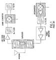
- One prior art implementation shown in Figure 1, includes a R x rejection filter in front of a two-stage power amplifier. Given that this node is at or near the noise floor, and given the amount of noise generated in the power amplifier, the amount of R x rejection required in the duplexer can be specified.
- the duplexer filter that implements the required rejection has an associated insertion loss. This loss is in the T x band, and is dependent upon the R x band rejection. Hence, the more rejection required, the higher the loss in the T x band.
- Receive band filtering between the last two stages of an N-stage power amplifier can reduce the R x band noise.
- N-1 interstage matching networks interposing N stage amplifiers, where N greater than or equal to 2.
- the interstage matching networks and stage amplifiers are electrically connected in series.
- the N-1 th or ultimate interstage matching network includes a T x band filter positioned proximate to the output of the penultimate or N-1 th stage power amplifier.
- the R x band noise dependency upon the T x chain is reduced so that the duplexer rejection requirement may be relaxed. As the loss is less, less power is required from the power amplifier. This is turn requires less current and results in longer battery life.
- FIG. 2 illustrates a transceiver 10 using an N-stage power amplifier of the present invention, where N ⁇ 2.
- An antenna 12 is connected to a duplexer 14.
- the duplexer 14 receives data from antenna 12 and transmits it to low noise amplifier (LNA) 16.
- a receive R x filter 18 is connected between LNA 16 and a downconverter 20.
- An IF filter 22 receives the output of downconverter 20.
- the duplexer 12 transmits data received from a power amplifier/filter 24.
- a transmit T x filter 26 connects between power amplifier/filter 24 and an upconverter 28.
- FIG. 3 illustrates a two-stage amplifier of the prior art.
- the interstage matching network is an RLC network.
- Figure 4 illustrates a novel power amplifier/filter 24, as shown in Figure 2. While a two-stage power amplifier is illustrated, this concept as will be described is easily extended to cover a N-stage power amplifier. In this illustration, N equals 2.
- the N-1 th interstage matching network includes a receive band filter positioned proximate to the output of the N-1 th stage power amplifier.
- the N-1 th interstage matching network has very low impedance.
- the receive band filter is designed to operate at the required impedance.
- the illustrative filter operates in a 6 ⁇ network. Approximately, 10dB of net rejection results in about 10dB reduction in the output R x band noise power.
- the receive band filter may be a surface acoustic wave filter, a film bulk acoustic resonator (FBAR) filter, a ceramic filter, or a piezo-electric based filter.
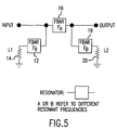
- Figure 5 illustrates a preferred embodiment of the interstage matching network shown in Figure 4.
- a first FBAR 12 is serially connected between the input and a first inductor 14 is tied to ground.
- a second FBAR 16 is connected between the input and output.
- a third FBAR 18 is connected between the output and a second inductor 20 that is tied to ground.
- the first and third FBARS 12, 18 have one resonant frequency while the second FBAR 16 has another resonant frequency.
- Figure 6 shows the noise reduction for a two stage power amplifier using the receive band filter shown in Figure 4 in the N-1 th interstage matching network.
- Figure 7 illustrates another preferred embodiment of the interstage matching network shown in Figure 4.
- a first FBAR 30 is connected between the input and second FBAR 32 that is connected to the output.
- a third and a fourth FBAR 34, 36 are connected to node A.
- An inductor 38 is connected between the third FBAR 34 and ground.
- Another inductor 40 is connected between the fourth FBAR 36 and ground.
- the first and second FBARS 30, 32 have one resonant frequency while the third and fourth FBARS 34, 36 have a different resonant frequency.
- Figure 8 illustrates another preferred embodiment of the interstage matching network shown in Figure 4.
- a first FBAR 42 is connected between the input and second FBAR 44 that is connected to the output.
- a third FBAR 46 is serially connected to an inductor 48.
- the first and second FBARs 24, 44 have one resonant frequency while the third FBAR 46 has a different resonant frequency.
Landscapes
- Engineering & Computer Science (AREA)
- Power Engineering (AREA)
- Amplifiers (AREA)
- Transmitters (AREA)
Abstract
Description
- The invention is related to the field of power amplifiers, particularly towards noise reduction in the power amplifiers.
- In a full duplex transceiver, both the transmitter and the receiver can operate simultaneously. This results in two forms of interference. The first interference is the Tx (transmit) band power getting into the receiver. The second interference is noise generated in the Rx (Receive) band by the Tx portion of the radio, and leaking into the Rx portion of the transceiver. Both types of interference are mitigated by using a duplexer. In this instance, a duplexer is a three port, passive element consisting of a pair of bandpass filters and supporting components. One filter passes the Tx frequencies and rejects the Rx. the other passes the Rx and rejects the Tx.
- As the transmit (Tx) power is not completely blocked by the duplexer, the power can enter the receiver thus causing distortion. In a filter-based duplexer, this is a measure of how well the receive (Rx) filter rejects the transmit Tx band power. The Tx filter has no effect because the leakage is in the pass-band of the Tx filter.
- The second interference is caused by noise in the Rx band, generated by the Tx circuitry, getting by the duplexer into the receiver. This causes a loss of sensitivity. In a filter-based duplexer, this is a measure of how well the Tx filter can reject the Rx band power. The Rx filter has no effect upon this leakage because it is in the pass-band of the Rx filter. This type of crosstalk drives the design of the Tx chain. The sensitivity required of the receiver dictates how much leakage is acceptable. The rejection of the duplexer dictates how much noise power the Tx chain can be allowed to generate.
- The noise figure of an amplifier is a sum all of its noise sources, referenced to the input of the amplifier. The noise power at the output of that amplifier is the sum of the gain of the amplifier and the noise figure. Since the sensitivity required by the Rx branch of the transceiver is set, the allowable noise power out of the Tx branch effectively sets the maximum gain of the power amplifier.
- In full duplex handsets, there is another constraint. The gain setting routine discussed above relies upon the Rx noise at the input to the power amplifier be at or near the noise floor available at that temperature. The noise generated in the Tx chain previous to the power amplifier must be sufficiently rejected to not increase the noise power at the output of the power amplifier. This is accomplished by inserting a Rx band reject filter just in front of the power amplifier, in the Tx band signal path. The difficulty of building this type of Rx rejection filter is such that many handsets rely upon two filters in parallel, each filter dealing with half the signal bandwidth, adding half the pass-band to the reject band frequency. This makes each filter of the pair much easier than a full band implementation. The input signal is routed through a switch, then into one of the filter pair. After the filter, the signal is then recombined with a switch.
- One prior art implementation, shown in Figure 1, includes a Rx rejection filter in front of a two-stage power amplifier. Given that this node is at or near the noise floor, and given the amount of noise generated in the power amplifier, the amount of Rx rejection required in the duplexer can be specified. The duplexer filter that implements the required rejection has an associated insertion loss. This loss is in the Tx band, and is dependent upon the Rx band rejection. Hence, the more rejection required, the higher the loss in the Tx band.
- Since the power output of the handset is constant, higher loss in the duplexer requires more power out of the power amplifier. At the high power levels required, higher power requires more current, thus, reducing battery life.
- Receive band filtering between the last two stages of an N-stage power amplifier can reduce the Rx band noise. There are N-1 interstage matching networks interposing N stage amplifiers, where N greater than or equal to 2. The interstage matching networks and stage amplifiers are electrically connected in series. The N-1th or ultimate interstage matching network includes a Tx band filter positioned proximate to the output of the penultimate or N-1th stage power amplifier.
-
- Figure 1 illustrates a functional block diagram for a full duplex transceiver of the prior art.
- Figure 2 illustrates a functional block diagram for a full duplex transceiver of the present invention.
- Figure 3 illustrates a functional block diagram for a power amplifier using a prior art interstage matching network.
- Figure 4 illustrates a functional block diagram for a power amplifier/
filter 24 shown in Figure 2. - Figure 5 illustrates an interstage matching network of the present invention shown in Figure 4.
- Figure 6 illustrates noise reduction for a two-stage power amplifier using receive band reject filter in the interstage matching network.
- Figure 7 illustrates another preferred embodiment of the interstage matching network shown in Figure 4.
- Figure 8 illustrates another preferred embodiment of the interstage matching network shown in Figure 4.
-
- In the present invention, the Rx band noise dependency upon the Tx chain is reduced so that the duplexer rejection requirement may be relaxed. As the loss is less, less power is required from the power amplifier. This is turn requires less current and results in longer battery life.
- Filtering between the two stages of the power amplifier can reduce the Rx band noise. In particular, either a band reject or a bandpass filter that rejects the Rx band will reduce the noise power. Figure 2 illustrates a
transceiver 10 using an N-stage power amplifier of the present invention, where N∃2. Anantenna 12 is connected to aduplexer 14. Theduplexer 14 receives data fromantenna 12 and transmits it to low noise amplifier (LNA) 16. A receive Rx filter 18 is connected betweenLNA 16 and adownconverter 20. AnIF filter 22 receives the output ofdownconverter 20. Theduplexer 12 transmits data received from a power amplifier/filter 24. A transmit Tx filter 26 connects between power amplifier/filter 24 and anupconverter 28. - Figure 3 illustrates a two-stage amplifier of the prior art. The interstage matching network is an RLC network.
- Figure 4 illustrates a novel power amplifier/
filter 24, as shown in Figure 2. While a two-stage power amplifier is illustrated, this concept as will be described is easily extended to cover a N-stage power amplifier. In this illustration, N equals 2. There are N-1 interstage matching networks interposing N stage amplifiers. The interstage matching networks and stage amplifiers are serially connected. The N-1th interstage matching network includes a receive band filter positioned proximate to the output of the N-1th stage power amplifier. - The N-1th interstage matching network has very low impedance. The receive band filter is designed to operate at the required impedance. The illustrative filter operates in a 6 Σ network. Approximately, 10dB of net rejection results in about 10dB reduction in the output Rx band noise power. The receive band filter may be a surface acoustic wave filter, a film bulk acoustic resonator (FBAR) filter, a ceramic filter, or a piezo-electric based filter.
- Figure 5 illustrates a preferred embodiment of the interstage matching network shown in Figure 4. A
first FBAR 12 is serially connected between the input and afirst inductor 14 is tied to ground. Asecond FBAR 16 is connected between the input and output. Athird FBAR 18 is connected between the output and asecond inductor 20 that is tied to ground. The first andthird FBARS second FBAR 16 has another resonant frequency. - Figure 6 shows the noise reduction for a two stage power amplifier using the receive band filter shown in Figure 4 in the N-1th interstage matching network.
- Figure 7 illustrates another preferred embodiment of the interstage matching network shown in Figure 4. At node A, a
first FBAR 30 is connected between the input andsecond FBAR 32 that is connected to the output. A third and afourth FBAR inductor 38 is connected between thethird FBAR 34 and ground. Anotherinductor 40 is connected between thefourth FBAR 36 and ground. The first andsecond FBARS fourth FBARS - Figure 8 illustrates another preferred embodiment of the interstage matching network shown in Figure 4. At node A, a
first FBAR 42 is connected between the input andsecond FBAR 44 that is connected to the output. Between node A and ground, athird FBAR 46 is serially connected to aninductor 48. The first andsecond FBARs third FBAR 46 has a different resonant frequency.
Claims (7)
- A power amplifier comprising:a series of N stage amplifiers, where N ≥2;a series of N-1 interstage networks interposing the series of N stage amplifiers, wherein the series of N-1 interstage networks and series of N stage amplifiers are electrically connected in series; and
wherein the N-1th interstage network includes a receive band reject filter positioned proximate to the output of the N-1th stage amplifier. - A power amplifier, as defined in claim 1, wherein the receive band reject filter is selected from a group that includes surface acoustic wave filters, film bulk acoustic resonators filters, ceramic filters, and piezo-electric based filters.
- A power amplifier, as defined in claim 1, wherein the N-1th interstage network has an input impedance that approximates the output impedance of the N-1th stage amplifier and has an output impedance that approximates the input impedance of the Nth stage amplifier.
- A power amplifier, as defined in claim 3, wherein the receive band reject filter has an impedance that is between the output impedance of the N-1th stage amplifier and the input impedance of the Nth stage amplifier.
- A power amplifier, as defined in claim 4, the receive band reject filter further comprising:a first film bulk acoustic resonator (12) connected between an input and the output of the N-1th stage amplifier;a second film bulk acoustic resonator (16) connected to the input;a first inductor (14) connecting between the second film bulk acoustic resonator and ground;a third film bulk acoustic resonator (18) connected to the output of the N-1th stage amplifier; anda second inductor (20) connecting between the third film bulk acoustic resonator and ground.
- A power amplifier, as defined in claim 4, the receive band reject filter further comprising:a first film bulk acoustic resonator (30) connected to an input;two paths, connected between the first film bulk acoustic resonator and ground, each path including a film bulk acoustic resonator (34, 36) serially connected to an inductor (38, 40); anda second film bulk acoustic resonator (32) connected between the first film bulk acoustic resonator and the output of the N-1th stage amplifier.
- A power amplifier, as defined in claim 4, the receive band reject filter further comprising:a first film bulk acoustic resonator (42) connected to an input;a film bulk acoustic resonator (46) serially connected to an inductor (48), connected between the first film bulk acoustic resonator and ground; anda second film bulk acoustic resonator (44) connected between the first film bulk acoustic resonator and the output of the N-1th stage amplifier.
Applications Claiming Priority (2)
| Application Number | Priority Date | Filing Date | Title |
|---|---|---|---|
| US678954 | 2000-10-03 | ||
| US09/678,954 US6489862B1 (en) | 2000-10-03 | 2000-10-03 | Method for reducing noise generated in a power amplifier |
Publications (1)
| Publication Number | Publication Date |
|---|---|
| EP1202447A1 true EP1202447A1 (en) | 2002-05-02 |
Family
ID=24725013
Family Applications (1)
| Application Number | Title | Priority Date | Filing Date |
|---|---|---|---|
| EP01112501A Withdrawn EP1202447A1 (en) | 2000-10-03 | 2001-05-22 | A method for reducing noise generated in a RF power amplifier |
Country Status (6)
| Country | Link |
|---|---|
| US (1) | US6489862B1 (en) |
| EP (1) | EP1202447A1 (en) |
| JP (1) | JP2002185262A (en) |
| KR (1) | KR20020026836A (en) |
| MY (1) | MY127331A (en) |
| SG (1) | SG108279A1 (en) |
Cited By (2)
| Publication number | Priority date | Publication date | Assignee | Title |
|---|---|---|---|---|
| KR20020026836A (en) * | 2000-10-03 | 2002-04-12 | 마리 오 휴버 | A method for reducing noise generated in a power amplifier |
| EP1505726A1 (en) * | 2003-08-01 | 2005-02-09 | Northrop Grumman Space & Missions Systems Corp. | Asymmetric, optimized common-source bi-directional amplifier |
Families Citing this family (22)
| Publication number | Priority date | Publication date | Assignee | Title |
|---|---|---|---|---|
| WO2003015260A1 (en) * | 2001-08-06 | 2003-02-20 | California Institute Of Technology | Method and apparatus for a multi-pole bandwidth enhancement technique for wideband amplification |
| US7113980B2 (en) | 2001-09-06 | 2006-09-26 | Bea Systems, Inc. | Exactly once JMS communication |
| US6924715B2 (en) * | 2002-02-12 | 2005-08-02 | Nortel Networks Limited | Band reject filters |
| US6710677B2 (en) * | 2002-02-12 | 2004-03-23 | Nortel Networks Limited | Band reject filters |
| US20050093652A1 (en) * | 2003-10-31 | 2005-05-05 | Qing Ma | Size scaling of film bulk acoustic resonator (FBAR) filters using impedance transformer (IT) or balun |
| CN101084623B (en) * | 2004-10-29 | 2012-02-01 | 北电网络有限公司 | band stop filter |
| US7274270B2 (en) | 2005-04-13 | 2007-09-25 | Avago Technologies Wireless Ip (Singapore) Pte. Ltd. | Resonator matching network |
| US7274275B2 (en) * | 2005-06-10 | 2007-09-25 | Avago Technologies Wireless Ip (Singapore) Pte. Ltd. | Bandpass filter network and method for bandpass filtering signals using multiple acoustic resonators |
| US7443269B2 (en) * | 2005-07-27 | 2008-10-28 | Avago Technologies General Ip (Singapore) Pte. Ltd. | Method and apparatus for selectively blocking radio frequency (RF) signals in a radio frequency (RF) switching circuit |
| US7372335B2 (en) * | 2005-10-21 | 2008-05-13 | Wilinx, Inc. | Wideband circuits and methods |
| US7598827B2 (en) * | 2006-06-19 | 2009-10-06 | Maxim Integrated Products | Harmonic termination of power amplifiers using BAW filter output matching circuits |
| US7586389B2 (en) * | 2006-06-19 | 2009-09-08 | Maxim Integrated Products, Inc. | Impedance transformation and filter using bulk acoustic wave technology |
| JP2008252249A (en) * | 2007-03-29 | 2008-10-16 | Mitsubishi Electric Corp | Ground station equipment for satellite communications |
| US7868703B2 (en) * | 2009-05-01 | 2011-01-11 | Raytheon Company | Passive spectrum control for pulsed RF power amplifiers |
| US9484887B2 (en) * | 2012-11-28 | 2016-11-01 | Telefonaktiebolaget Lm Ericsson (Publ) | Acoustic wave band reject filter |
| WO2015001828A1 (en) | 2013-07-01 | 2015-01-08 | 株式会社村田製作所 | Front-end circuit |
| WO2015045538A1 (en) * | 2013-09-26 | 2015-04-02 | 株式会社村田製作所 | High frequency power amplifier, high frequency front end circuit, and wireless communication device |
| WO2015186577A1 (en) * | 2014-06-02 | 2015-12-10 | 株式会社村田製作所 | Transmission circuit, high-frequency front-end circuit, transmission signal control method, and high-frequency front-end transmission/reception control method |
| US10396750B2 (en) | 2016-08-26 | 2019-08-27 | Samsung Electro-Mechanics Co., Ltd. | Radio frequency transmitter having improved receive band rejection function |
| KR102323572B1 (en) | 2017-05-16 | 2021-11-05 | 삼성전기주식회사 | Multi-band radio-frequency transmitter with receiving band variable filtering function |
| WO2022080393A1 (en) * | 2020-10-14 | 2022-04-21 | 株式会社村田製作所 | Power amplifier circuit and communication device |
| WO2024057696A1 (en) * | 2022-09-16 | 2024-03-21 | 株式会社村田製作所 | High frequency circuit and communication apparatus |
Citations (5)
| Publication number | Priority date | Publication date | Assignee | Title |
|---|---|---|---|---|
| US5051706A (en) * | 1988-11-09 | 1991-09-24 | Kabushiki Kaisha Toshiba | High frequency power amplifier circuit |
| US5438683A (en) * | 1992-03-02 | 1995-08-01 | Novatel Communications, Ltd. | Automatic level control circuit for dual mode analog/digital cellular telephone |
| EP0862266A2 (en) * | 1997-02-12 | 1998-09-02 | Oki Electric Industry Co., Ltd. | Surface-acoustic-wave filters with poles of attenuation created by impedance circuits |
| WO2000024124A1 (en) * | 1998-10-22 | 2000-04-27 | Ericsson, Inc. | Dual-band, dual-mode power amplifier with reduced power loss |
| US6122491A (en) * | 1996-12-27 | 2000-09-19 | Lucent Technologies Inc. | Communications system using power amplifier with dynamic biasing |
Family Cites Families (10)
| Publication number | Priority date | Publication date | Assignee | Title |
|---|---|---|---|---|
| US4792939A (en) * | 1986-01-24 | 1988-12-20 | Hitachi Denshi Kabushiki Kaisha | Duplex radio communication transceiver |
| JP2533497B2 (en) * | 1986-08-13 | 1996-09-11 | 株式会社日立製作所 | Power control method |
| JPH04306922A (en) * | 1991-04-04 | 1992-10-29 | Nec Corp | Radio equipment for common use in microwave band transmission and reception |
| JP2855989B2 (en) * | 1992-08-31 | 1999-02-10 | 日本電気株式会社 | High frequency signal amplifier circuit |
| KR100534159B1 (en) * | 1995-06-09 | 2006-01-27 | 마쯔시다덴기산교 가부시키가이샤 | Amplifier |
| WO1997013320A1 (en) * | 1995-09-29 | 1997-04-10 | Matsushita Electric Industrial Co., Ltd. | Power amplifier and communication device |
| JPH09219667A (en) * | 1996-02-13 | 1997-08-19 | Murata Mfg Co Ltd | Spread spectrum communication transmitter |
| US6078794A (en) * | 1997-02-19 | 2000-06-20 | Motorola, Inc. | Impedance matching for a dual band power amplifier |
| JP2000138546A (en) * | 1998-10-30 | 2000-05-16 | Kyocera Corp | High frequency multi-stage power amplifier |
| US6489862B1 (en) * | 2000-10-03 | 2002-12-03 | Agilent Technologies, Inc. | Method for reducing noise generated in a power amplifier |
-
2000
- 2000-10-03 US US09/678,954 patent/US6489862B1/en not_active Expired - Lifetime
-
2001
- 2001-05-22 EP EP01112501A patent/EP1202447A1/en not_active Withdrawn
- 2001-05-29 MY MYPI20012543 patent/MY127331A/en unknown
- 2001-09-28 KR KR1020010060334A patent/KR20020026836A/en not_active Ceased
- 2001-09-29 SG SG200106027A patent/SG108279A1/en unknown
- 2001-10-03 JP JP2001307449A patent/JP2002185262A/en not_active Withdrawn
Patent Citations (5)
| Publication number | Priority date | Publication date | Assignee | Title |
|---|---|---|---|---|
| US5051706A (en) * | 1988-11-09 | 1991-09-24 | Kabushiki Kaisha Toshiba | High frequency power amplifier circuit |
| US5438683A (en) * | 1992-03-02 | 1995-08-01 | Novatel Communications, Ltd. | Automatic level control circuit for dual mode analog/digital cellular telephone |
| US6122491A (en) * | 1996-12-27 | 2000-09-19 | Lucent Technologies Inc. | Communications system using power amplifier with dynamic biasing |
| EP0862266A2 (en) * | 1997-02-12 | 1998-09-02 | Oki Electric Industry Co., Ltd. | Surface-acoustic-wave filters with poles of attenuation created by impedance circuits |
| WO2000024124A1 (en) * | 1998-10-22 | 2000-04-27 | Ericsson, Inc. | Dual-band, dual-mode power amplifier with reduced power loss |
Cited By (3)
| Publication number | Priority date | Publication date | Assignee | Title |
|---|---|---|---|---|
| KR20020026836A (en) * | 2000-10-03 | 2002-04-12 | 마리 오 휴버 | A method for reducing noise generated in a power amplifier |
| EP1505726A1 (en) * | 2003-08-01 | 2005-02-09 | Northrop Grumman Space & Missions Systems Corp. | Asymmetric, optimized common-source bi-directional amplifier |
| US7239852B2 (en) | 2003-08-01 | 2007-07-03 | Northrop Grumman Corporation | Asymmetric, optimized common-source bi-directional amplifier |
Also Published As
| Publication number | Publication date |
|---|---|
| KR20020026836A (en) | 2002-04-12 |
| MY127331A (en) | 2006-11-30 |
| SG108279A1 (en) | 2006-01-27 |
| US6489862B1 (en) | 2002-12-03 |
| JP2002185262A (en) | 2002-06-28 |
Similar Documents
| Publication | Publication Date | Title |
|---|---|---|
| US6489862B1 (en) | Method for reducing noise generated in a power amplifier | |
| CN103503314B (en) | MEMS tunable notch filter frequency automatic control loop system and method | |
| US8462755B2 (en) | Duplexer/multiplexer having filters that include at least one band reject filter | |
| KR100951482B1 (en) | Band reject filters | |
| CN107689778B (en) | High-frequency module and communication device | |
| US8207799B2 (en) | Band reject filters | |
| US6603372B1 (en) | Laminated notch filter and cellular phone using the same | |
| US20080101263A1 (en) | Single-ended to differential duplexer filter | |
| US10128796B2 (en) | Power amplification module and front end circuit | |
| JP2002198765A (en) | Integrated filter balun | |
| JP2010022007A (en) | Full-duplex transceiver with distributed duplexing function | |
| US6229408B1 (en) | Zero loss bias “T” | |
| US20130241674A1 (en) | Elastic wave filter device and communication apparatus equipped with the same | |
| JP2000349591A (en) | A duplexer using a surface acoustic wave filter. | |
| JP3337073B2 (en) | Surface acoustic wave device | |
| CN116803005A (en) | Filters with multiple outputs or inputs for achieving multiple filter frequency responses | |
| US6958663B2 (en) | In-band group delay equalizer and distortion compensation amplifier | |
| JPH0983214A (en) | Antenna duplexer | |
| US11637734B2 (en) | Radio-frequency circuit, communication device, and radio-frequency circuit designing method | |
| US7420440B2 (en) | Transmitting filter including SAW resonators | |
| JP3549831B2 (en) | Laminated notch filter and mobile phone using the same | |
| US7352262B2 (en) | Insulation of anti-resonance in resonators | |
| JP4963376B2 (en) | Bandpass filter network and method for bandpass filtering a signal using a plurality of acoustic resonators | |
| US6861925B2 (en) | Surface acoustic wave filter | |
| KR101643582B1 (en) | If band-pass filter |
Legal Events
| Date | Code | Title | Description |
|---|---|---|---|
| PUAI | Public reference made under article 153(3) epc to a published international application that has entered the european phase |
Free format text: ORIGINAL CODE: 0009012 |
|
| AK | Designated contracting states |
Kind code of ref document: A1 Designated state(s): AT BE CH CY DE DK ES FI FR GB GR IE IT LI LU MC NL PT SE TR |
|
| AX | Request for extension of the european patent |
Free format text: AL;LT;LV;MK;RO;SI |
|
| AKX | Designation fees paid | ||
| REG | Reference to a national code |
Ref country code: DE Ref legal event code: 8566 |
|
| 17P | Request for examination filed |
Effective date: 20021002 |
|
| RBV | Designated contracting states (corrected) |
Designated state(s): DE FR GB IT |
|
| 17Q | First examination report despatched |
Effective date: 20050404 |
|
| RAP1 | Party data changed (applicant data changed or rights of an application transferred) |
Owner name: AVAGO TECHNOLOGIES WIRELESS IP (SINGAPORE) PTE. LT |
|
| STAA | Information on the status of an ep patent application or granted ep patent |
Free format text: STATUS: THE APPLICATION HAS BEEN WITHDRAWN |
|
| 18W | Application withdrawn |
Effective date: 20070115 |