EP1202350A2 - Semiconductor device and manufacturing method thereof - Google Patents
Semiconductor device and manufacturing method thereof Download PDFInfo
- Publication number
- EP1202350A2 EP1202350A2 EP01308569A EP01308569A EP1202350A2 EP 1202350 A2 EP1202350 A2 EP 1202350A2 EP 01308569 A EP01308569 A EP 01308569A EP 01308569 A EP01308569 A EP 01308569A EP 1202350 A2 EP1202350 A2 EP 1202350A2
- Authority
- EP
- European Patent Office
- Prior art keywords
- glass plate
- supporting substrate
- substrate
- semiconductor device
- adhesive resin
- Prior art date
- Legal status (The legal status is an assumption and is not a legal conclusion. Google has not performed a legal analysis and makes no representation as to the accuracy of the status listed.)
- Granted
Links
Images


Classifications
-
- H—ELECTRICITY
- H10—SEMICONDUCTOR DEVICES; ELECTRIC SOLID-STATE DEVICES NOT OTHERWISE PROVIDED FOR
- H10W—GENERIC PACKAGES, INTERCONNECTIONS, CONNECTORS OR OTHER CONSTRUCTIONAL DETAILS OF DEVICES COVERED BY CLASS H10
- H10W42/00—Arrangements for protection of devices
- H10W42/80—Arrangements for protection of devices protecting against overcurrent or overload, e.g. fuses or shunts
-
- H—ELECTRICITY
- H10—SEMICONDUCTOR DEVICES; ELECTRIC SOLID-STATE DEVICES NOT OTHERWISE PROVIDED FOR
- H10W—GENERIC PACKAGES, INTERCONNECTIONS, CONNECTORS OR OTHER CONSTRUCTIONAL DETAILS OF DEVICES COVERED BY CLASS H10
- H10W76/00—Containers; Fillings or auxiliary members therefor; Seals
- H10W76/10—Containers or parts thereof
- H10W76/12—Containers or parts thereof characterised by their shape
- H10W76/15—Containers comprising an insulating or insulated base
- H10W76/153—Containers comprising an insulating or insulated base having interconnections in passages through the insulating or insulated base
-
- H—ELECTRICITY
- H10—SEMICONDUCTOR DEVICES; ELECTRIC SOLID-STATE DEVICES NOT OTHERWISE PROVIDED FOR
- H10W—GENERIC PACKAGES, INTERCONNECTIONS, CONNECTORS OR OTHER CONSTRUCTIONAL DETAILS OF DEVICES COVERED BY CLASS H10
- H10W76/00—Containers; Fillings or auxiliary members therefor; Seals
- H10W76/60—Seals
-
- H—ELECTRICITY
- H10—SEMICONDUCTOR DEVICES; ELECTRIC SOLID-STATE DEVICES NOT OTHERWISE PROVIDED FOR
- H10W—GENERIC PACKAGES, INTERCONNECTIONS, CONNECTORS OR OTHER CONSTRUCTIONAL DETAILS OF DEVICES COVERED BY CLASS H10
- H10W72/00—Interconnections or connectors in packages
- H10W72/01—Manufacture or treatment
- H10W72/0198—Manufacture or treatment batch processes
-
- H—ELECTRICITY
- H10—SEMICONDUCTOR DEVICES; ELECTRIC SOLID-STATE DEVICES NOT OTHERWISE PROVIDED FOR
- H10W—GENERIC PACKAGES, INTERCONNECTIONS, CONNECTORS OR OTHER CONSTRUCTIONAL DETAILS OF DEVICES COVERED BY CLASS H10
- H10W72/00—Interconnections or connectors in packages
- H10W72/50—Bond wires
- H10W72/551—Materials of bond wires
- H10W72/552—Materials of bond wires comprising metals or metalloids, e.g. silver
- H10W72/5522—Materials of bond wires comprising metals or metalloids, e.g. silver comprising gold [Au]
Definitions
- the present invention relates to a semiconductor device that includes a semiconductor element for high frequency applications and an overcurrent-protectingfunctionin a hollow airtight package and a method of manufacturing the same.
- FIG.9 An example of the semiconductor device employing the hollow package in the conventional art is shown in FIG.9.
- This electronic parts comprise a base substrate 1 formed of ceramic, etc., a lead 2 for external connection, and a cap 3 formed similarly of ceramic.
- a semiconductor chip 5 is adhered onto a surface of an element mounting portion 4 of the lead 2, then the semiconductor chip 5 and the lead 2 are connected via bonding wires 6, and then the semiconductor chip 5 is sealed in an airtight space 7 constructed by the cap 3 (for example, Patent Application Publication Hei 10-173117).
- Such parts are manufactured via steps of preparing the lead 2 in the form of a lead frame, then bonding the semiconductor chip 5 to the lead frame via die bonding or wire bonding, then mounting the base substrate 1 on a bottom surface of the lead frame, then mounting the cap 3 on the base substrate 1 to put the leads 2 between them, and then cutting/shaping the leads 2.
- a semiconductor device of the present invention has been made in view of the above circumstances, and comprises a supporting substrate made of insulating material, a conductive pattern provided on a surface of the supporting substrate, and external connecting terminals provided on a back surface and connected electrically to the conductive pattern, a circuit element provided on the conductive pattern, a glass plate adhered to cover the circuit element and to form an airtight hollow portion between the supporting substrate and the glass plate, and an adhesive resin applied to an overall adhered surface of the glass plate.
- the semiconductor device of the present invention has such a feature that, since the light-shielding adhesive resin is applied to the overall adhesive surface of the glass plate that is used to house the circuit element in the airtight hollow space, the state of the adhered portion can be checked by the visual inspection and also the direct incidence of the light onto the circuit element can be prevented, whereby the change in the characteristic of the circuit element can be avoided in structure.
- the semiconductor device manufacturing method of the present invention is characterized by comprising a step of preparing a supporting substrate in which a conductive pattern having a large number of mounting portions is provided and external connecting terminals are provided on a back surface, a step of adhering the circuit element onto the mounting portions respectively, a step of applying an adhesive resin to an overall adhesive surface of a glass plate that covers the circuit element and forms an airtight hollow portion between the supporting substrate and the glass plate every mounting portion, a step of adhering the supporting substrate and the glass plate to form the airtight hollow portion every mounting portion, and a step of separating the supporting substrate every mounting portion by dicing adhered portions between the supporting substrate and the glass plate.
- the semiconductor device manufacturing method of the present invention has such a feature that, since the light-shielding adhesive resin is previously applied to the overall adhesive surface of the glass plate that forms the airtight hollow space in the step of forming the airtight hollow space, a plurality of semiconductor elements can be formed at a time, whereby the manufacturing steps can be simplified and the mass production can be carried out.
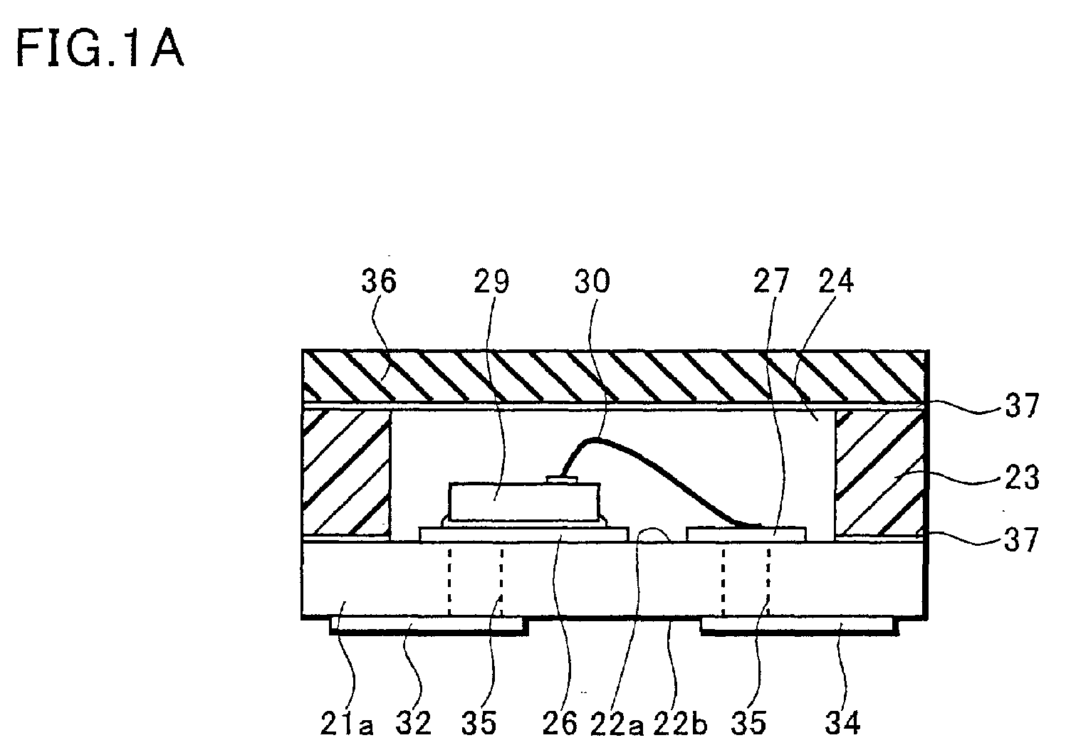
- FIG.1A is a sectional view and FIG.1B is a plan view showing an embodiment of the semiconductor device of the present invention.
- a substrate 21a divided from a large-sized substrate 21 is formed of insulatingmaterial such as ceramic, glass epoxy, etc., and has a plate thickness of 100 to 300 ⁇ m and a rectangular shape whose long side x short side is about 2.5 mm x 1.9 mm when it is viewed as a plan view (viewed as shown in FIG.1B).
- the substrate 21a has a first main face 22a on the surface side and a second main face 22b on the back surface side respectively, and these faces extend in parallel with each other.
- a column portion 23 is an pillar portion that is provided on an outer periphery of the substrate 21a to have a height of about 0.4 mm and a width of about 0.5 mm.
- a concave portion 24 is formed on the center portion of the substrate 21a by the column portion 23.
- the substrate 21a and the column portion 23 both are formed as separate members are adhered by the adhesive 37. In this case, the substrate 21a and the column portion 23 both are integrated together previously may be employed.
- a surface of the first main face 22a of the substrate 21a is formed flat, and an island portion 26 and electrode portions 27, 28 are formed on the surface by conductive patterns such as the gold plating, or the like.
- a semiconductor chip 29 such as a Schottky barrier diode, a MOSFET element, or the like, for example, is die-bonded to the island portion 26 of the substrate 21a.
- An electrode pad formed on a surface of the semiconductor chip 29 and the electrode portions 27, 28 are connected by bonding wires 30.
- External connecting terminals 32, 33, 34 are formed on the surface of the second main face 22b of the substrate 21a by the conductive patterns such as the gold plating, or the like.
- a via hole 35 that passes through the substrate 21a from the first main face 22a to the second main face 22b is provided in the electrode portions 32, 33, 34.
- An inside of the via hole 35 is filled with conductive material such as tungsten, silver, copper, or the like, so that the island portion 26, the electrode portion 27, and the electrode portion 28 are connected electrically to the external connecting terminal 32, the external connecting terminal 33, and the external connecting terminal 34 respectively.
- End portions of the external connecting terminals 32, 33, 34 are retreated from the end portion of the substrate 21a by about 0.01 to 0.1 mm.
- the bonding wire 30 should be connected to avoid the upper surfaces of the via holes 35 of the electrode portion 27, 28 respectively.
- the external connecting terminals 32, 33, 34 are formed in advance on the large-sized substrate 21.
- a transparent glass plate 36 having a plate thickness of about 0.1 to 0.3 mm is employed as a lid member. Since the glass plate 36 covers a number of concave portions 24 formed on the large-sized substrate 21, the light-shielding adhesive resin 37 is previously applied to the overall adhered surface of the glass plate 36. Also, since the upper portion of the column portion 23 forming the concave portion 24 and the adhered surface of the glass plate 36 are adhered, the semiconductor chip 29 and the metal thin wire 30 can be housed perfectly in the airtight space.
- the light-shielding adhesive resin 37 is applied to the overall adhered surface of the glass plate 36, the light that transmits the glass plate 36 can be cut off by the light-shielding adhesive resin 37 and thus the light does not directly enter into the semiconductor chip 29, etc. in the concave portion 24.
- the column portion 23 cut by the dicing surrounds the peripheral area of the semiconductor chip 29, and the cut glass plate 36 closes tightly the upper area thereof.
- the column portion 23 and the first main face 22a of the substrate 21a are adhered by the adhesive 37, and the column portion 23 and the glass plate 36 are adhered by the adhesive 37.
- the semiconductor chip 29 and the metal thin wires 30 are housed in the airtight space constructed by the concave portion 24.
- Outer peripheral end surfaces of the substrate 21a, the column portion 23, and the glass plate 36 are cut by the dicing so as to form flat cut end surfaces.
- the above semiconductor device is mounted such that the external connecting terminals 32, 33, 34 are opposed/adhered to the electrode patterns on the packaging substrate.
- the large-sized substrate in which a plurality of mounting portions are arranged in a matrix fashion, e.g., 100 portions are arranged in 10 rows and 10 columns, on the substrate having the plate thickness of 200 to 350 ⁇ m that can maintain the mechanical strength during the manufacturing steps is prepared.
- the substrate is an insulating substrate made of ceramic, glass epoxy, or the like.
- the semiconductor chips are die-bonded to respective mounting portions and then all semiconductor chips are covered with the common resin layer by dropping (potting) epoxy liquid resin by a predetermined amount.
- potting dropping
- potting potting
- a surface of the resin layer is worked into a flat surface by grinding curved surfaces.
- the grind apparatus is used to grind the surface of the resin layer by the grind blade such that the surface of the resin layer has a uniform height from the substrate.
- a film thickness of the resin layer is formed to 0.3 to 1.0 mm.
- FIG.2A is a sectional view and FIG.2B a plan view showing an embodiment of an overcurrent-protecting device using a fuse.
- a substrate 51 is formed of insulating material such as ceramic, glass epoxy, etc.
- the substrate 51 has a plate thickness of 100 to 300 ⁇ m and a rectangular shape whose long side x short side is about 2.5 mm x 1.9 mm when it is viewed as a plan view (viewed as shown in FIG.2B).
- the substrate 51 has a first main face 52a on the surface side and a second main face 52b on the back surface side respectively.
- a column portion 53 is an side portion that is provided on an outer periphery of the substrate 51 to have a height of about 0.4 mm and a width of about 0.5 mm.
- a concave portion 54 is formed on the center portion of the substrate 51 by the column portion 53.
- the substrate 51 and the column portion 53 both are formed. as separate members are adhered by the adhesive 61.
- the substrate 51 and the column portion 53 both are integrated together previously may be employed.
- a surface of the first main face 52a of the substrate 51 is formed flat, and electrode portions 55, 56 are formed on the surface by conductive patterns such as the gold plating, or the like.
- a metal thin wire 57 having a diameter of 30 ⁇ m, for example, is provided between the electrode portions 55, 56 by the wire bonding.
- the metal thin wire 57 is formed of a gold wire having a purity of 99.99 %, a solder thin wire, or the like.
- the metal thin wire 57 is first bonded to the electrode portion 55 and is second bonded to the electrode portion 56 such that a wire loop is formed to have a height smaller than a height of the concave portion 54.
- External connecting terminals 58, 59 are formed on the surface of the second main face 52b of the substrate 51 by the conductive patterns such as the gold plating, or the like.
- a via hole 60 passing through the substrate 51 is provided under the electrode portions 55, 56 respectively.
- An inside of the via hole 60 is filled with conductive material such as tungsten, or the like, so that the electrode portion 55 and the electrode portion 56 are connected electrically to the external connecting terminal 58 and the external connecting terminal 59 respectively.
- End portions of the external connecting terminals 58, 59 are retreated from the end portion of the substrate 51 by about 0.01 to 0.1 mm.
- the bonding wire 57 should be connected to avoid the upper surfaces of the via holes 60 of the electrode portion 55, 56 respectively.
- a transparent glass plate 62 having a plate thickness of about 0.1 to 0.3 mm is employed as a lid member. Since the glass plate 62 covers a number of concave portions 54 formed on the large-sized substrate 21, the light-shielding adhesive resin 61 is previously applied to the overall adhered surface of the glass plate 62. Also, since the upper portion of the column portion 53 forming the concave portion 54 and the adhered surface of the glass plate 62 are adhered, the metal thin wire 57 can be housed perfectly in the airtight space.
- the light-shielding adhesive resin 61 is applied to the overall adhered surface of the glass plate 62, the light that transmits the glass plate 62 can be cut off by the light-shielding-adhesive resin 61 and thus the light does not directly enter into the metal thin wire 57, etc. in the concave portion 54.
- the above overcurrent-protecting device is mounted such that the external connecting terminals 58, 59 are opposed/adhered to the electrode patterns on the packaging substrate.
- an overcurrent in excess of the rated current is flown between the external connecting terminals 58, 59, such overcurrent flows through the metal thin wire 57 to cause the rapid temperature rise due to the specific resistance of the metal thin wire 57.
- the metal thin wire 57 is melt down by this heat generation to perform a protection function against the overcurrent. If a gold (Au) wire having the diameter of 30 ⁇ m and a wire length of about 0.7 mm is employed, the fusing current is about 4 A (1 to 5 seconds).
- the metal thin wire 57 is melt down in its middle portion rather than its end portions close to the electrode portions 55, 56. At this time, since the fused portion does not contact to other material such as the resin, the device in which the ignition; the emitting smoke, the change of color, and the deformation are not generated in appearance can be obtained. Also, since the metal thin wire 57 is melted down, the device in which both terminals are disconnected perfectly at the time of the overcurrent can be formed.
- the fuse element can be formed by forming a part of the conductive patterns constituting the electrode portions 55, 56 as a narrow wedge-like shape successively, by adhering a polysilicon resistor to the metal thin wire, or the like in addition to the metal thin wire.
- any means may be employed if the fused portion is housed in the concave portion 54.
- the concave portion 54 is airtightly closed in the air, the incombustible gas to form the nitrogen atmosphere, etc., for example, can be filled therein.
- the transparent glass plate 36 is employed to seal the semiconductor chip 29, the bonding wires 30, etc. airtightly in the hollow space, the state of the adhered portion between the glass plate 36 and the column portion 23 can be checked by the visual inspection. Also, since the light-shielding adhesive resin 37 is applied to the entire adhered surface of the glass plate 36, there can be prevented such an event that the light that transmits through the glass plate 36, enters into the concave portion 24 and directly enters into the semiconductor chip 29, etc. and thus the degradation of the characteristic of the semiconductor chip 29, etc. is caused.
- the hollow structure can be formed by employing the column portion 23 and the glass plate 36, and also the semiconductor chip 29, etc. that are die-bonded onto the substrate 21a are housed in the airtight space constructed by the concave portion 24 as the hollow portion. Accordingly, a material cost can be lowered extremely in contrast to the case where the substrate 21a is covered with the resin layer and therefore the semiconductor chips 29 adhered onto the mounting portions are covered with the resin layer.
- the hollow structure can be formed by using the column portion 23 and the glass plate 36 and also the step of planarizing the surface of the semiconductor element is not needed because the glass plate 36 is employed as the lid body of the hollow structure. Therefore, a production cost can be lowered extremely rather than the case where the substrate 21a is covered with the resin layer and therefore the semiconductor chips 29 adhered onto the mounting portions are covered with the resin layer.
- the via holes 35 passing through the substrate 21a from the first main face 22a to the second main face 22b are formed in the substrate 21a. Then, the insides of the via holes 35 are filled with the conductive material such as tungsten, silver, copper, etc., and also the island portion 26, the electrode portion 27, and the electrode portion 28 are connected electrically to the external connecting terminals 32, 33, 34 respectively, so that internal elements and the external connecting terminals can be connected electrically with no lead that is extended from the substrate 21a to the outside. Therefore, a packaging area can be reduced extremely when the semiconductor device is packaged onto the printed board.
- a first manufacturing method of the semiconductor device shown in FIG.1 will be explained in detail hereinafter.
- the large-sized substrate 21 is prepared.
- the large-sized substrate 21 is formed of insulating material such as ceramic, glass epoxy, etc. and has a plate thickness of 100 to 300 ⁇ m. Also, the large-sized substrate 21 has the first main face 22a on the surface side and the second main face 22b on the back surface side respectively.
- a symbol 23 is a lattice-like column portion having a height of 0.1 to 0.5 mm and a constant width of about 0.25 to 0.5 mm, and forms the concave portion 24 in which the center portion of the substrate 21 is depressed by the column portion 23.
- the substrate 21 and the column portion 23 are formed integrally in advance to form the above plate thickness including the column portion 23. In this case, the structure in which the substrate 21 and the column portion 23 are formed individually and then adhered/fixed together may be prepared.
- the concave portions 24 each having a size of about 0.8 mm x 0.6 mm, for example, are arranged at an equal distance vertically and laterally on the substrate 21. A large number of sets of the island portions 26 and the electrode portions 27, 28 are drawn on the first main faces 22a of the concave portions 24 by the conductive patterns formed of the gold plating. The concave portion 24 and a part of the column portion 23 of the substrate 21 surrounding the concave portion 24 constitute the element mounting portion 41.
- the semiconductor chip 29 is die-bonded to the island portion 26 every concave portion 24 and the bonding wire 30 is wire-bonded. Then, one sides of the bonding wires 30 that are wire-bonded to the semiconductor chip 29 are connected to the electrode portions 27, 28. A loop height of the bonding wire 30 at this time is set to a height that is lower than a height of the column portion 23.
- the transparent glass plate 36 having a plate thickness of about 0.1 to 0.3 mm is prepared, and then the light- shielding adhesive resin 37 is applied to the overall adhered surface of the glass plate 36. Then, the glass plate 36 is adhered as a lid member that constitutes the hollow airtight structures on the mounting portions 41 including a plurality of concave portions 24 that are formed by using the large-sized substrate 21 and the column portions 23. Accordingly, the semiconductor chip 29 and the bonding wire 30 can be perfectly housed in the airtight space. At this time, as described above, since the light-shielding adhesive resin 37 is applied to the overall surface of the glass plate 36, a large quantity of semiconductor elements can be formed at a time.
- the column portion 23 may be adhered to the large-sized substrate 21 later, otherwise the large-sized substrate 21 and the column portion 23 may be integrally formed together previously. Also, the concave portions 24 may be formed by digging the large-sized substrate 21.
- individual devices shown in FIG.5 can be obtained by dividing the substrate 21 into respective mounting portions 41 basedon alignment marks formed on the surface of the substrate 21.
- a dicing blade 42 is used to divide, and a dicing sheet is pasted on the back surface side of the substrate 21 and then the substrate 21 and the glass plate 36 are collectively cut away along dicing lines 43 vertically and laterally.
- the dicing line 43 is positioned in the center of the column portion 23.
- the dicing sheet may be pasted on the glass plate 36 side and then the dicing may be applied from the second main face 22b side.
- the large-sized flat substrate 21 is prepared.
- the large-sized substrate 21 is formed of insulating material such as ceramic, glass epoxy, etc. and has a plate thickness of 100 to 300 ⁇ m.
- the large-sized substrate 21 has the first main face 22a on the surface side and the second main face 22b on the back surface side respectively.
- a large number of sets of the island portions 26 and the electrode portions 27, 28 are drawn on the surface of the first main faces 22a by the conductive patterns formed of the gold plating.
- the area that surrounds the island portion 26 and the electrode portions 27, 28 constitutes the element mounting portion 41.
- a large number of element mounting portions 41 are arranged at an equal distance vertically and laterally.
- the semiconductor chip 29 is die-bonded to the island portion 26 every element mounting portion 41 and the bonding wire 30 is wire-bonded. Then, one sides of the bonding wires 30 that are wire-bonded to the semiconductor chip 29 are connected to the electrode portions 27, 28. A loop height of the bonding wire 30 at this time is set to a height that is smaller than a depth of the concave portion 24.
- the second substrate 21a having the concave portions 24 (through holes) at positions that correspond to the element mounting portions 41 is adhered/fixed to the surface of the first main face 22a on the substrate 21 to which the die bonding and the wire bonding have been applied.
- the adhesive such as epoxy adhesive, etc. is employed to adhere.
- the concave portions 24 each having a size of about 0.8 mm x 0.6 mm, for example, are arranged at an equal distance vertically and laterally on the second substrate 21b.
- the column portion 23 having a height of about 0.1 to 0.2 mm and a width of about 0.2 to 0.5 mm is provided between the concave portions 24 so as to surround the concave portion 24 in a lattice fashion.
- the island 26, the semiconductor chip 29, the electrode portions 27, 28, etc. are exposed from the concave portion 24, which is equivalent to the state in FIG.3B.
- the die bonding and the wire bonding can be applied to the flat substrate 21, the contact between the vacuum collet or the bonding tool and the column portion 23 can be eliminated and thus a dimension of the concave portion 24 can be reduced.
- the transparent glass plate 36 having a plate thickness of about 0.1 to 0.3 mm is prepared, and then the light- shielding adhesive resin 37 is applied to the overall adhered surface of the glass plate 36. Then, the glass plate 36 is adhered as a lid member that constitutes the hollow airtight structures on the mounting portions 41 including a plurality of concave portions 24 that are formed by using the large-sized substrate 21 and the column portions 23. As a result, the semiconductor chip 29 and the bonding wire 30 can be perfectly housed in the airtight space. At this time, as described above, since the light-shielding adhesive resin 37 is applied to the overall surface of the glass plate 36, a large quantity of semiconductor elements can be formed at a time.
- individual devices shown in FIG.8B can be obtained by dividing the substrate 21 into respective mounting portions 41 based on alignment marks formed on the surface of the substrate 21.
- the dicing blade 42 is used to divide, and the dicing sheet is pasted on the second main face 22b side of the substrate 21 and then the substrate 21, the second substrate 21b, and the glass plate 36 are collectively cut away along the dicing lines 43 vertically and laterally.
- the dicing line 43 is positioned in the center of the column portion 23.
- the dicing may be applied from the second main face 22b side.
- the transparent glass plate is employed to seal the semiconductor chip, the bonding wires, etc. airtightly in the hollow space, the state of the adhered portion between the glass plate and the column portion can be checked by the visual inspection. Also, since the light-shielding adhesive resin is applied to the entire surface of the adhered surface of the glass plate, there can be prevented such an event that the light that transmits through the glass plate, enters into the concave portion and directly enters into the semiconductor chip, etc. and thus the degradation of the characteristic of the semiconductor chip, etc. is caused.
- the semiconductor device manufacturing method of the present invention since the light-shielding adhesive resin is previously applied to the overall adhesive surface of the glass plate that forms the hollow airtight structure, the semiconductor element, etc. can be adhered at a time onto a number of concave portions that are constructed by the substrate and the column portions. Therefore, the fabrication cost can be reduced extremely and the mass production can be carried out.
Landscapes
- Solid State Image Pick-Up Elements (AREA)
- Light Receiving Elements (AREA)
- Structures Or Materials For Encapsulating Or Coating Semiconductor Devices Or Solid State Devices (AREA)
Abstract
Description
Claims (6)
- A semiconductor device comprising:a supporting substrate made of insulating material;a conductive pattern provided on a surface of the supporting substrate;an external connecting terminal provided on a back surface of the supporting substrate and electrically connected to the conductive patterns;a circuit element provided on the conductive pattern;a glass plate that covers the circuit element and that forms a hollow airtight portion between the supporting substrate and the glass plate; andan adhesive resin applied to an overall adhered surface of the glass plate.
- A semiconductor device according to claim 1, wherein the adhesive resin is formed of a light-shielding adhesive resin.
- A semiconductor device according to claim 1 or 2 wherein the circuit element includes a semiconductor element or a fuse element.
- A semiconductor device manufacturing method comprising steps of:preparing a supporting substrate in which a conductive pattern having a large number of mounting portions on a surface of the supporting substrate is provided and external connecting terminals are provided on a back surface;fixing the circuit element onto the mounting portions respectively;applying an adhesive resin to an overall adhesive surface of a glass plate that covers the circuit element and forms an airtight hollow portion between the supporting substrate and the glass plate every mounting portion;adhering the supporting substrate and the glass plate to form the airtight hollow portion every mounting portion; anddividing the supporting substrate into respective mounting portions by dicing adhered portions between the supporting substrate and the glass plate.
- A semiconductor device manufacturing method comprising steps of:preparing a supporting substrate in which conductive patterns having a number of mounting portions thereon are provided on a surface of the supporting substrate and external connecting terminals are provided on a back surface of the supporting substrate;fixing a circuit element onto respective mounting portions;mounting a lattice-like column member on the supporting substrate;applying an adhesive resin to an overall adhesive surface of a glass plate that covers the circuit element and forms an airtight hollow portion between the supporting substrate and the glass plate every mounting portion;adhering a glass plate onto the column member to cover the circuit element and to form a hollow airtight portion formed by the supporting substrate, the column member and the glass plate every mounting portion; anddividing the supporting substrate into respective mounting portions by dicing adhered portions between the supporting substrate and the glass plate.
- A semiconductor device manufacturing method according to claim 4 or 5, wherein the adhesive resin is formed of a light-shielding adhesive resin.
Applications Claiming Priority (2)
| Application Number | Priority Date | Filing Date | Title |
|---|---|---|---|
| JP2000308620A JP4565727B2 (en) | 2000-10-10 | 2000-10-10 | Manufacturing method of semiconductor device |
| JP2000308620 | 2000-10-10 |
Publications (3)
| Publication Number | Publication Date |
|---|---|
| EP1202350A2 true EP1202350A2 (en) | 2002-05-02 |
| EP1202350A3 EP1202350A3 (en) | 2004-03-31 |
| EP1202350B1 EP1202350B1 (en) | 2007-01-10 |
Family
ID=18788900
Family Applications (1)
| Application Number | Title | Priority Date | Filing Date |
|---|---|---|---|
| EP20010308569 Expired - Lifetime EP1202350B1 (en) | 2000-10-10 | 2001-10-08 | Semiconductor device and manufacturing method thereof |
Country Status (5)
| Country | Link |
|---|---|
| US (1) | US6815808B2 (en) |
| EP (1) | EP1202350B1 (en) |
| JP (1) | JP4565727B2 (en) |
| CN (1) | CN1207779C (en) |
| DE (1) | DE60125888T2 (en) |
Families Citing this family (23)
| Publication number | Priority date | Publication date | Assignee | Title |
|---|---|---|---|---|
| EP1369929B1 (en) * | 2002-05-27 | 2016-08-03 | STMicroelectronics Srl | A process for manufacturing encapsulated optical sensors, and an encapsulated optical sensor manufactured using this process |
| JP2004055860A (en) * | 2002-07-22 | 2004-02-19 | Renesas Technology Corp | Method for manufacturing semiconductor device |
| DE10237084A1 (en) * | 2002-08-05 | 2004-02-19 | Osram Opto Semiconductors Gmbh | Electrically conductive frame with a semiconductor light diode, to illuminate a mobile telephone keypad, has a layered structure with the electrical connections and an encapsulated diode chip in very small dimensions |
| TWI239080B (en) * | 2002-12-31 | 2005-09-01 | Advanced Semiconductor Eng | Semiconductor chip package and method for the same |
| CN100366700C (en) * | 2003-02-25 | 2008-02-06 | 株式会社钟化 | Curable composition and method for preparing same, light-shielding paste, light-shielding resin and method for forming same, package for light-emitting diode, and semiconductor device |
| US8110899B2 (en) * | 2006-12-20 | 2012-02-07 | Intel Corporation | Method for incorporating existing silicon die into 3D integrated stack |
| US7605462B2 (en) * | 2007-02-23 | 2009-10-20 | Powertech Technology Inc. | Universal substrate for a semiconductor device having selectively activated fuses |
| US20100164677A1 (en) * | 2008-12-29 | 2010-07-01 | Chin-Chi Yang | Fuse |
| JP2010199474A (en) * | 2009-02-27 | 2010-09-09 | Kyocera Chemical Corp | Hollow package for electronic component, adhesive sheet for hollow package for electronic component, lid body, and electronic component manufacturing method |
| JP2012039031A (en) * | 2010-08-11 | 2012-02-23 | Nitto Denko Corp | Light emitting device |
| JP5981183B2 (en) * | 2012-03-23 | 2016-08-31 | 矢崎総業株式会社 | Display device |
| JP5813552B2 (en) | 2012-03-29 | 2015-11-17 | 株式会社東芝 | Semiconductor package and manufacturing method thereof |
| US11211305B2 (en) | 2016-04-01 | 2021-12-28 | Texas Instruments Incorporated | Apparatus and method to support thermal management of semiconductor-based components |
| US10861796B2 (en) | 2016-05-10 | 2020-12-08 | Texas Instruments Incorporated | Floating die package |
| US10179730B2 (en) | 2016-12-08 | 2019-01-15 | Texas Instruments Incorporated | Electronic sensors with sensor die in package structure cavity |
| US9929110B1 (en) | 2016-12-30 | 2018-03-27 | Texas Instruments Incorporated | Integrated circuit wave device and method |
| US10074639B2 (en) | 2016-12-30 | 2018-09-11 | Texas Instruments Incorporated | Isolator integrated circuits with package structure cavity and fabrication methods |
| US10411150B2 (en) | 2016-12-30 | 2019-09-10 | Texas Instruments Incorporated | Optical isolation systems and circuits and photon detectors with extended lateral P-N junctions |
| US9865537B1 (en) * | 2016-12-30 | 2018-01-09 | Texas Instruments Incorporated | Methods and apparatus for integrated circuit failsafe fuse package with arc arrest |
| US10121847B2 (en) | 2017-03-17 | 2018-11-06 | Texas Instruments Incorporated | Galvanic isolation device |
| JP6635605B2 (en) * | 2017-10-11 | 2020-01-29 | 国立研究開発法人理化学研究所 | Current introduction terminal, pressure holding device and X-ray imaging device having the same |
| KR102592329B1 (en) * | 2018-06-26 | 2023-10-20 | 삼성전자주식회사 | Fabrication method of semiconductor package |
| CN119069450A (en) * | 2024-11-04 | 2024-12-03 | 杭州暖芯迦电子科技有限公司 | Device for continuous blood glucose monitoring and method of manufacturing the same |
Family Cites Families (26)
| Publication number | Priority date | Publication date | Assignee | Title |
|---|---|---|---|---|
| JPS60239043A (en) * | 1984-05-14 | 1985-11-27 | Oki Electric Ind Co Ltd | Manufacture of package for semiconductor device |
| JPH0744261B2 (en) * | 1988-12-28 | 1995-05-15 | 凸版印刷株式会社 | Transparent coating for semiconductor devices |
| US5160787A (en) | 1989-01-12 | 1992-11-03 | Mitsubishi Gas Chemical Company, Inc. | Electrical laminate having ability to absorb ultraviolet rays |
| US5105260A (en) * | 1989-10-31 | 1992-04-14 | Sgs-Thomson Microelectronics, Inc. | Rf transistor package with nickel oxide barrier |
| JP2967215B2 (en) * | 1990-10-12 | 1999-10-25 | 株式会社村田製作所 | Manufacturing method of chip-type electronic components |
| US5327443A (en) * | 1991-10-30 | 1994-07-05 | Rohm Co., Ltd. | Package-type semiconductor laser device |
| US5277356A (en) * | 1992-06-17 | 1994-01-11 | Rohm Co., Ltd. | Wire bonding method |
| JPH07225391A (en) * | 1994-02-14 | 1995-08-22 | Toshiba Corp | LCD display module |
| US5382310A (en) * | 1994-04-29 | 1995-01-17 | Eastman Kodak Company | Packaging medical image sensors |
| US5590787A (en) * | 1995-01-04 | 1997-01-07 | Micron Technology, Inc. | UV light sensitive die-pac for securing semiconductor dies during transport |
| JPH08242046A (en) * | 1995-03-03 | 1996-09-17 | Rohm Co Ltd | Structure of semiconductor device with thermal fuse |
| JP3423855B2 (en) * | 1996-04-26 | 2003-07-07 | 株式会社デンソー | Electronic component mounting structure and electronic component mounting method |
| JP2933038B2 (en) | 1996-12-09 | 1999-08-09 | 日本電気株式会社 | Hollow package and manufacturing method thereof |
| US6117705A (en) * | 1997-04-18 | 2000-09-12 | Amkor Technology, Inc. | Method of making integrated circuit package having adhesive bead supporting planar lid above planar substrate |
| JPH1131751A (en) * | 1997-07-10 | 1999-02-02 | Sony Corp | Hollow package and manufacturing method thereof |
| JPH1197656A (en) * | 1997-09-22 | 1999-04-09 | Fuji Electric Co Ltd | Semiconductor optical sensor device |
| DE19752196C1 (en) | 1997-11-25 | 1999-02-11 | Siemens Ag | Semiconductor component, especially smart switch in car and industrial electronics |
| JP3339397B2 (en) * | 1998-01-20 | 2002-10-28 | 日本電気株式会社 | Method for manufacturing semiconductor device |
| US6020633A (en) * | 1998-03-24 | 2000-02-01 | Xilinx, Inc. | Integrated circuit packaged for receiving another integrated circuit |
| US6111199A (en) * | 1998-04-07 | 2000-08-29 | Integrated Device Technology, Inc. | Integrated circuit package using a gas to insulate electrical conductors |
| US5923958A (en) | 1998-05-28 | 1999-07-13 | Pan Pacific Semiconductor Co., Ltd. | Method for semiconductor chip packaging |
| GB9818474D0 (en) | 1998-08-26 | 1998-10-21 | Hughes John E | Multi-layer interconnect package for optical devices & standard semiconductor chips |
| JP3408987B2 (en) * | 1999-03-30 | 2003-05-19 | 三菱電機株式会社 | Semiconductor device manufacturing method and semiconductor device |
| JP2000311959A (en) * | 1999-04-27 | 2000-11-07 | Sanyo Electric Co Ltd | Semiconductor device and manufacturing method thereof |
| US6525397B1 (en) * | 1999-08-17 | 2003-02-25 | National Semiconductor Corporation | Extended drain MOSFET for programming an integrated fuse element to high resistance in low voltage process technology |
| US6507264B1 (en) * | 2000-08-28 | 2003-01-14 | Littelfuse, Inc. | Integral fuse for use in semiconductor packages |
-
2000
- 2000-10-10 JP JP2000308620A patent/JP4565727B2/en not_active Expired - Fee Related
-
2001
- 2001-09-26 US US09/963,267 patent/US6815808B2/en not_active Expired - Lifetime
- 2001-10-08 EP EP20010308569 patent/EP1202350B1/en not_active Expired - Lifetime
- 2001-10-08 DE DE2001625888 patent/DE60125888T2/en not_active Expired - Fee Related
- 2001-10-10 CN CNB011354089A patent/CN1207779C/en not_active Expired - Fee Related
Also Published As
| Publication number | Publication date |
|---|---|
| CN1207779C (en) | 2005-06-22 |
| JP2002118192A (en) | 2002-04-19 |
| US6815808B2 (en) | 2004-11-09 |
| DE60125888T2 (en) | 2007-11-15 |
| JP4565727B2 (en) | 2010-10-20 |
| DE60125888D1 (en) | 2007-02-22 |
| CN1347153A (en) | 2002-05-01 |
| US20020041016A1 (en) | 2002-04-11 |
| EP1202350A3 (en) | 2004-03-31 |
| EP1202350B1 (en) | 2007-01-10 |
Similar Documents
| Publication | Publication Date | Title |
|---|---|---|
| US6815808B2 (en) | Hollow airtight semiconductor device package | |
| US6285067B1 (en) | Electronic device and method for manufacturing the same | |
| KR100241573B1 (en) | Semiconductor wafer | |
| US4974057A (en) | Semiconductor device package with circuit board and resin | |
| US20190035837A1 (en) | Solid image-pickup device with flexible circuit substrate | |
| US6365433B1 (en) | Semiconductor device and manufacturing method thereof | |
| US20080296717A1 (en) | Packages and assemblies including lidded chips | |
| US20060065964A1 (en) | Semiconductor device comprising light-emitting element and light-receiving element, and manufacturing method therefor | |
| US20240128713A1 (en) | Package structure | |
| JPH11186301A (en) | Method for manufacturing semiconductor device | |
| CN102468194A (en) | Semiconductor device packaging method and semiconductor device package | |
| US6838765B2 (en) | Semiconductor device and manufacturing method thereof | |
| JP4605880B2 (en) | Semiconductor device | |
| JP3462806B2 (en) | Semiconductor device and manufacturing method thereof | |
| JP3269025B2 (en) | Semiconductor device and manufacturing method thereof | |
| JP2000156434A (en) | Semiconductor device | |
| JP4475788B2 (en) | Manufacturing method of semiconductor device | |
| EP0081419A2 (en) | High lead count hermetic mass bond integrated circuit carrier | |
| JP2002050720A (en) | Method for manufacturing semiconductor device | |
| JPH0723961Y2 (en) | Package for storing semiconductor devices | |
| JPH069509Y2 (en) | Package for storing semiconductor devices | |
| JP2002050590A (en) | Method for manufacturing semiconductor device | |
| JP2001044313A (en) | Method for manufacturing semiconductor device | |
| JP2000164609A (en) | Method for manufacturing semiconductor device |
Legal Events
| Date | Code | Title | Description |
|---|---|---|---|
| PUAI | Public reference made under article 153(3) epc to a published international application that has entered the european phase |
Free format text: ORIGINAL CODE: 0009012 |
|
| AK | Designated contracting states |
Kind code of ref document: A2 Designated state(s): AT BE CH CY DE DK ES FI FR GB GR IE IT LI LU MC NL PT SE TR |
|
| AX | Request for extension of the european patent |
Free format text: AL;LT;LV;MK;RO;SI |
|
| PUAL | Search report despatched |
Free format text: ORIGINAL CODE: 0009013 |
|
| AK | Designated contracting states |
Kind code of ref document: A3 Designated state(s): AT BE CH CY DE DK ES FI FR GB GR IE IT LI LU MC NL PT SE TR |
|
| AX | Request for extension of the european patent |
Extension state: AL LT LV MK RO SI |
|
| RIC1 | Information provided on ipc code assigned before grant |
Ipc: 7H 01L 23/552 A |
|
| 17P | Request for examination filed |
Effective date: 20040603 |
|
| 17Q | First examination report despatched |
Effective date: 20040709 |
|
| AKX | Designation fees paid |
Designated state(s): DE FR GB |
|
| GRAP | Despatch of communication of intention to grant a patent |
Free format text: ORIGINAL CODE: EPIDOSNIGR1 |
|
| GRAS | Grant fee paid |
Free format text: ORIGINAL CODE: EPIDOSNIGR3 |
|
| GRAA | (expected) grant |
Free format text: ORIGINAL CODE: 0009210 |
|
| AK | Designated contracting states |
Kind code of ref document: B1 Designated state(s): DE FR GB |
|
| REG | Reference to a national code |
Ref country code: GB Ref legal event code: FG4D |
|
| REF | Corresponds to: |
Ref document number: 60125888 Country of ref document: DE Date of ref document: 20070222 Kind code of ref document: P |
|
| ET | Fr: translation filed | ||
| PLBE | No opposition filed within time limit |
Free format text: ORIGINAL CODE: 0009261 |
|
| STAA | Information on the status of an ep patent application or granted ep patent |
Free format text: STATUS: NO OPPOSITION FILED WITHIN TIME LIMIT |
|
| 26N | No opposition filed |
Effective date: 20071011 |
|
| PGFP | Annual fee paid to national office [announced via postgrant information from national office to epo] |
Ref country code: DE Payment date: 20081014 Year of fee payment: 8 |
|
| PGFP | Annual fee paid to national office [announced via postgrant information from national office to epo] |
Ref country code: FR Payment date: 20081014 Year of fee payment: 8 |
|
| PGFP | Annual fee paid to national office [announced via postgrant information from national office to epo] |
Ref country code: GB Payment date: 20081008 Year of fee payment: 8 |
|
| REG | Reference to a national code |
Ref country code: FR Ref legal event code: ST Effective date: 20100630 |
|
| PG25 | Lapsed in a contracting state [announced via postgrant information from national office to epo] |
Ref country code: DE Free format text: LAPSE BECAUSE OF NON-PAYMENT OF DUE FEES Effective date: 20100501 Ref country code: FR Free format text: LAPSE BECAUSE OF NON-PAYMENT OF DUE FEES Effective date: 20091102 |
|
| PG25 | Lapsed in a contracting state [announced via postgrant information from national office to epo] |
Ref country code: GB Free format text: LAPSE BECAUSE OF NON-PAYMENT OF DUE FEES Effective date: 20091008 |