EP1200325B1 - Methods to manufacture single cell and multi-cell regenerative photoelectrochemical devices - Google Patents
Methods to manufacture single cell and multi-cell regenerative photoelectrochemical devices Download PDFInfo
- Publication number
- EP1200325B1 EP1200325B1 EP00912270A EP00912270A EP1200325B1 EP 1200325 B1 EP1200325 B1 EP 1200325B1 EP 00912270 A EP00912270 A EP 00912270A EP 00912270 A EP00912270 A EP 00912270A EP 1200325 B1 EP1200325 B1 EP 1200325B1
- Authority
- EP
- European Patent Office
- Prior art keywords
- substrate
- film
- layer
- protective film
- patterned
- Prior art date
- Legal status (The legal status is an assumption and is not a legal conclusion. Google has not performed a legal analysis and makes no representation as to the accuracy of the status listed.)
- Expired - Lifetime
Links
Images


Classifications
-
- H—ELECTRICITY
- H01—ELECTRIC ELEMENTS
- H01M—PROCESSES OR MEANS, e.g. BATTERIES, FOR THE DIRECT CONVERSION OF CHEMICAL ENERGY INTO ELECTRICAL ENERGY
- H01M14/00—Electrochemical current or voltage generators not provided for in groups H01M6/00 - H01M12/00; Manufacture thereof
- H01M14/005—Photoelectrochemical storage cells
-
- C—CHEMISTRY; METALLURGY
- C03—GLASS; MINERAL OR SLAG WOOL
- C03C—CHEMICAL COMPOSITION OF GLASSES, GLAZES OR VITREOUS ENAMELS; SURFACE TREATMENT OF GLASS; SURFACE TREATMENT OF FIBRES OR FILAMENTS MADE FROM GLASS, MINERALS OR SLAGS; JOINING GLASS TO GLASS OR OTHER MATERIALS
- C03C17/00—Surface treatment of glass, not in the form of fibres or filaments, by coating
- C03C17/34—Surface treatment of glass, not in the form of fibres or filaments, by coating with at least two coatings having different compositions
- C03C17/3411—Surface treatment of glass, not in the form of fibres or filaments, by coating with at least two coatings having different compositions with at least two coatings of inorganic materials
- C03C17/3417—Surface treatment of glass, not in the form of fibres or filaments, by coating with at least two coatings having different compositions with at least two coatings of inorganic materials all coatings being oxide coatings
-
- H—ELECTRICITY
- H01—ELECTRIC ELEMENTS
- H01G—CAPACITORS; CAPACITORS, RECTIFIERS, DETECTORS, SWITCHING DEVICES OR LIGHT-SENSITIVE DEVICES, OF THE ELECTROLYTIC TYPE
- H01G9/00—Electrolytic capacitors, rectifiers, detectors, switching devices, light-sensitive or temperature-sensitive devices; Processes of their manufacture
- H01G9/20—Light-sensitive devices
- H01G9/2027—Light-sensitive devices comprising an oxide semiconductor electrode
- H01G9/2031—Light-sensitive devices comprising an oxide semiconductor electrode comprising titanium oxide, e.g. TiO2
-
- H—ELECTRICITY
- H01—ELECTRIC ELEMENTS
- H01G—CAPACITORS; CAPACITORS, RECTIFIERS, DETECTORS, SWITCHING DEVICES OR LIGHT-SENSITIVE DEVICES, OF THE ELECTROLYTIC TYPE
- H01G9/00—Electrolytic capacitors, rectifiers, detectors, switching devices, light-sensitive or temperature-sensitive devices; Processes of their manufacture
- H01G9/20—Light-sensitive devices
- H01G9/2068—Panels or arrays of photoelectrochemical cells, e.g. photovoltaic modules based on photoelectrochemical cells
-
- C—CHEMISTRY; METALLURGY
- C03—GLASS; MINERAL OR SLAG WOOL
- C03C—CHEMICAL COMPOSITION OF GLASSES, GLAZES OR VITREOUS ENAMELS; SURFACE TREATMENT OF GLASS; SURFACE TREATMENT OF FIBRES OR FILAMENTS MADE FROM GLASS, MINERALS OR SLAGS; JOINING GLASS TO GLASS OR OTHER MATERIALS
- C03C2217/00—Coatings on glass
- C03C2217/40—Coatings comprising at least one inhomogeneous layer
- C03C2217/425—Coatings comprising at least one inhomogeneous layer consisting of a porous layer
-
- C—CHEMISTRY; METALLURGY
- C03—GLASS; MINERAL OR SLAG WOOL
- C03C—CHEMICAL COMPOSITION OF GLASSES, GLAZES OR VITREOUS ENAMELS; SURFACE TREATMENT OF GLASS; SURFACE TREATMENT OF FIBRES OR FILAMENTS MADE FROM GLASS, MINERALS OR SLAGS; JOINING GLASS TO GLASS OR OTHER MATERIALS
- C03C2217/00—Coatings on glass
- C03C2217/70—Properties of coatings
- C03C2217/71—Photocatalytic coatings
-
- H—ELECTRICITY
- H01—ELECTRIC ELEMENTS
- H01M—PROCESSES OR MEANS, e.g. BATTERIES, FOR THE DIRECT CONVERSION OF CHEMICAL ENERGY INTO ELECTRICAL ENERGY
- H01M6/00—Primary cells; Manufacture thereof
- H01M6/14—Cells with non-aqueous electrolyte
- H01M6/18—Cells with non-aqueous electrolyte with solid electrolyte
- H01M6/188—Processes of manufacture
-
- H—ELECTRICITY
- H01—ELECTRIC ELEMENTS
- H01M—PROCESSES OR MEANS, e.g. BATTERIES, FOR THE DIRECT CONVERSION OF CHEMICAL ENERGY INTO ELECTRICAL ENERGY
- H01M6/00—Primary cells; Manufacture thereof
- H01M6/40—Printed batteries, e.g. thin film batteries
-
- H—ELECTRICITY
- H10—SEMICONDUCTOR DEVICES; ELECTRIC SOLID-STATE DEVICES NOT OTHERWISE PROVIDED FOR
- H10K—ORGANIC ELECTRIC SOLID-STATE DEVICES
- H10K71/00—Manufacture or treatment specially adapted for the organic devices covered by this subclass
- H10K71/10—Deposition of organic active material
- H10K71/12—Deposition of organic active material using liquid deposition, e.g. spin coating
- H10K71/13—Deposition of organic active material using liquid deposition, e.g. spin coating using printing techniques, e.g. ink-jet printing or screen printing
-
- Y—GENERAL TAGGING OF NEW TECHNOLOGICAL DEVELOPMENTS; GENERAL TAGGING OF CROSS-SECTIONAL TECHNOLOGIES SPANNING OVER SEVERAL SECTIONS OF THE IPC; TECHNICAL SUBJECTS COVERED BY FORMER USPC CROSS-REFERENCE ART COLLECTIONS [XRACs] AND DIGESTS
- Y02—TECHNOLOGIES OR APPLICATIONS FOR MITIGATION OR ADAPTATION AGAINST CLIMATE CHANGE
- Y02E—REDUCTION OF GREENHOUSE GAS [GHG] EMISSIONS, RELATED TO ENERGY GENERATION, TRANSMISSION OR DISTRIBUTION
- Y02E10/00—Energy generation through renewable energy sources
- Y02E10/50—Photovoltaic [PV] energy
- Y02E10/542—Dye sensitized solar cells
-
- Y—GENERAL TAGGING OF NEW TECHNOLOGICAL DEVELOPMENTS; GENERAL TAGGING OF CROSS-SECTIONAL TECHNOLOGIES SPANNING OVER SEVERAL SECTIONS OF THE IPC; TECHNICAL SUBJECTS COVERED BY FORMER USPC CROSS-REFERENCE ART COLLECTIONS [XRACs] AND DIGESTS
- Y02—TECHNOLOGIES OR APPLICATIONS FOR MITIGATION OR ADAPTATION AGAINST CLIMATE CHANGE
- Y02P—CLIMATE CHANGE MITIGATION TECHNOLOGIES IN THE PRODUCTION OR PROCESSING OF GOODS
- Y02P70/00—Climate change mitigation technologies in the production process for final industrial or consumer products
- Y02P70/50—Manufacturing or production processes characterised by the final manufactured product
Definitions
- This invention relates to single cell and multi-cell regenerative photovoltaic photoelectrochemical (RPEC) devices, and to materials and methods used for manufacture of such devices.
- RPEC photovoltaic photoelectrochemical
- RPEC cells as of the type disclosed in the above patterns, are capable of being fabricated in a laminate arrangement between two large area substrates without undue expense.
- One typical arrangement involves two glass substrates, each utilising an electrically conducting coating upon the internal surface of the substrate.
- Another typical arrangement involves the first substrate being glass or polymeric and utilising an electrically conducting coating upon the internal surface of the substrate, with the second substrate being polymeric.
- the internal surface of said second polymeric substrate is coated with an electrically conducting coating
- said second polymeric substrate comprises a polymeric foil laminate, utilising adjacent electrically conductive material, such as carbon.
- the external surface may be a laminated metal film, and in other arrangements, the external surface may be coated by a metal.
- At least one of said first and second substrates is substantially transparent to visible light, as is the attached transparent electrically conducting (TEC) coating.
- RPEC cells contain a photoanode, typically comprising a ruthenium dye-sensitised, nanoporous semiconducting oxide (eg. titania) layer attached to one conductive coating, and a cathode, typically comprising a redox electrocatalyst layer attached to the other conductive coating or conductive material.
- An electrolyte containing a redox mediator is located between the photoanode and cathode, and the electrolyte is sealed from the environment.
- the photoanode and the cathode are typically electrically separated by a porous insulating layer (eg. insulating ceramic oxides) or spacer(s) (eg. insulating spheres).
- TEC coatings which usually comprise a metal oxide(s), have high resistivity when compared with normal metal conductors, resulting in high resistive losses for large area RPEC cells operating under high illumination.
- one method to minimise these losses is the deposition of one or more networks of electrically conductive material that serve to collect and/or distribute electrons in the cell.
- RPEC modules Another method to minimise these losses is by connecting a multiple of RPEC cells (here called 'RPEC modules') in series to generate higher voltages and to minimise total current.
- Such connections in RPEC modules may be made externally or internally (International Application PCT/AU00/00190 ).
- selected areas of such conducting coatings must be electrically isolated, portions of such areas overlapped when laminated, interconnects used to connect such overlapped areas and electrolyte-impermeable barriers used to separate the electrolyte of individual cells.
- Titanium dioxide or similar semiconductor
- an electrocatalyst is screen printed onto selected areas of the TEC coating of the other substrate.
- the titanium dioxide titanium dioxide (titania) is coated with a thin layer of a dye by immersion of the titania-coated substrate in the dye solution. strips of sealant and interconnect material are deposited upon one of the substrates and the two substrates are then bonded together. Electrolyte is added to the cells via access apertures in one of the substrates and these apertures are then sealed.
- an RPEC module involves the use of one substrate with a TEC-coating that has been divided into electrically isolated regions. Successive layers of titania, insulating ceramic oxide, and conducting catalytic material (for example, carbon-based) are deposited, for example by screen printing, onto selected areas of the TEC-coated substrate, with the catalytic layer also serving as an interconnect.
- the titania is coated with a thin layer of the dye by immersion of the multiple-coated substrate in the dye solution.
- Electrolyte is added to the spaces within the porous titania-insulator-catalytic layers. The sealant face of a sealant/polymer and/or metal foil laminate is sealed to the substrate.
- One process that prevents dye adsorption to the conductive coating involves covering relevant areas of the conducting coating with a polymeric film, application of dye to the coated substrate and then removal of the polymeric film, thus leaving a clean conductive coating surface to which a subsequent seal may be made.
- Another process that prevents dye adsorption to the conductive coating involves use of a laminated film (eg. surlyn/polypropylene) in which one face (eg. the surlyn face) is sealed to the relevant areas of the conducting coating, after which the dye is applied to the coated substrate and then the upper layer (eg. polypropylene) is removed, thus leaving a clean polymer (eg. surlyn) surface to which a subsequent seal may be made.
- a laminated film eg. surlyn/polypropylene
- This subsequent seal may involve additional sealant material or may involve sealing directly to the sealant surface, with the seal being made to a coated glass substrate or to a polymeric foil laminate, such as surlyn/aluminium.
- these protective film processes are inconvenient and time consuming and can result in variability in performance of the RPEC.
- An additional impediment to a continuous manufacturing process is that dye application to the semiconducting oxide needs to be automated to be carried out efficiently, preferably within a low volume container that may be dark, heated, and provided with a partially sealed, low-oxygen content atmosphere.
- the present invention provides a method for manufacturing regenerative photoelectrochemical (RPEC) devices in a production line, each device being deposited on a substrate, the method comprising the steps of:
- the protective film may comprise a patterned composite, laminated or multilayer film (CLM film) and the substrate may be a multiply-coated substrate of RPEC cells and modules.
- CLM film patterned composite, laminated or multilayer film
- the protective film may be patterned to create apertures, which are used as engagement means and the step of transporting the substrate comprises penetrating the engagement means with teeth to locate and mechanically engage the film in transportation of the film/substrate composite.
- the method allows continuous and convenient transport of the CLM film/substrate composite, using the engagement means, through one or more steps of the manufacturing process, including, but not limited to application of dye to the semiconductor oxide, addition of electrolyte, continuous removal of part of said patterned CLM film and sealing of the multiply-coated substrate to another substrate.
- the patterned film has the advantage of preventing adsorption of dye on the predetermined areas of said substrate. A portion of the part of said patterned film not removed may be utilised as sealant to subsequently bond the substrates of the RPEC cells and modules.
- the present invention provides for application of a continuous patterned CLM film to a multiply-coated substrate of RPEC cells and modules, and continuous and convenient transport of the patterned film/substrate composite through one or more steps of the manufacturing process, including, but not limited to application of dye to the semiconductor oxide, addition of electrolyte, continuous removal of part of said patterned CLM film and sealing of the multiply-coated substrate to another substrate.
- the patterned film may be a laminate of two or more polymers plus the option of an external layer of metallic or other materials, whereby one of the external layers of the laminate will function as the sealant of the RPEC device.
- the other layer(s) of the laminate function to prevent access of the dye, electrolyte, solvents and/or other materials to one face of the sealant layer.
- the patterned film may be dispensed in a substantially continuous sheet, preferably from a roll, and may be continuously patterned using stamping, rolling or any of the known methods of such patterning, to remove portions of film, thereby leaving apertures, hereby termed access regions, and optionally also leaving other apertures, hereby termed engagement means.
- a sealant face of said patterned film and/or predetermined areas of the surface of the multiply-coated substrate are treated with an adhesion promoting means, such as an adhesion primer, corona discharge or other known processes, in order to effect superior adhesion of said treated face and/or said treated surface in the subsequent bonding process.
- the substrate may be bonded to said patterned film by using roller, hot roller, stamping, or hot stamping processes, or by any of the known methods of such bonding. Particular care must be taken in the bonding process to ensure desired alignment of multiply-coated areas of said substrates with said access regions of said patterned film.
- Said access regions enable access to at least one selected area of said substrate, by dye solutions, electrolyte, solvents, gases and such like materials in subsequent steps of said continuous manufacturing process.
- Mechanical contact is made with said patterned film in order to transport said patterned film attached to the substrate i.e. the "film/substrate composite", through subsequent steps of said continuous manufacturing process.
- Said mechanical contact may comprise any of the known methods of mechanical contact used to transport a film.
- Said mechanical contact includes, but is not limited to penetration of said engagement means by projections that are then moved to effect said transport, whereby said projections include, but are not limited to teeth of sprockets, teeth in linear placement as in racks, hooks, supports and such like mechanical devices as are known to those of ordinary skill in the art.
- Said sprockets may be round, or essentially triangular, square, polygonal or of any suitable shape, and the apertures comprising the engagement means may be square, round or of any suitable shape, and may form one or more lines along the length of said patterned film.
- Said mechanical contact may include, but is not limited to opposing sets of rollers touching said film that passes between said sets of rollers, and with first set of rollers moved in opposite rotation to second set of rollers in order to transport said film in the desired direction.
- Said patterned film/substrate composite may be transported through a dye application chamber that may be dark, heated, and provided with a partially sealed, low-oxygen content atmosphere.
- said patterned film/substrate composite may be transported through the dye solution in a zig-zag manner, linearly, or in any other manner to provide effective use of the solution and space.
- Said dye solution may be agitated, such as by bubbles, stirring, pumping, ultrasonics or other known means of agitation.
- Said patterned film/substrate composite may be transported through a rinsing chamber, an electrolyte chamber, and other chambers, including but not limited to drying chambers. Part of said patterned film may then be removed in a continuous process, leaving the sealant layer of the patterned film adhering to regions of said multiply-coated substrate.
- Said mechanical contact with said sealant layer film enables convenient transport of said sealant film/substrate composite through subsequent steps of said continuous manufacturing process, including sealing of exposed surface of clean sealant on said multiply-coated substrate to a second substrate.
- Said multiply-coated substrate may comprise a TEC-coated glass substrate or a polymeric substrate, upon which subsequent layers of material are deposited.
- Said second substrate may comprise a TEC-coated glass substrate, a polymeric substrate, or a polymeric/metal foil laminate, such as surlyn/aluminium, whereby part of the polymeric layer (eg. surlyn) of said polymeric/metal foil laminate (eg. surlyn/aluminium) is bonded to said remaining patterned polymeric film (eg. surlyn) that is adhering to regions of the multiply-coated substrate.
- polymeric substrates and polymeric/metal foil laminates may be dispensed in a substantially continuous sheet, preferably from a roll.
- a CLM film (1a) is dispensed from a roll (1b) and is subjected to a patterning process (2) whereby portions of film are removed, leaving a patterned CLM film (1c) with access regions (1d) and engagement means in the form of apertures (1e), as shown in Figure 2 .
- the patterned CLM film (1a) is then treated with adhesion promoters (3) as are selected areas of the surfaces of the multiply-coated glass substrates (3).
- the multiply-coated substrates are then bonded (4,5) to the continuous patterned CLM film (1a), ensuring desired alignment of multiply-coated areas of the substrates with the access regions of the patterned CLM film.
- the patterned CLM film/substrate composite is then transported through subsequent steps of the continuous manufacturing process by mechanical contact of sprocket teeth with the engagement means of the patterned CLM film.
- the patterned CLM film/substrate composite is then transported through a low volume dyeing chamber (6) that is dark, heated, and provided with a partially sealed, low-oxygen content atmosphere.
- the patterned CLM film/substrate composite is transported through a stirred dye solution in a zig-zag manner as shown in Figure 3 .
- the patterned CLM film/substrate composite is then transported through a chamber (7) where the composite is rinsed, dried and exposed to electrolyte solution.
- the upper layer of the patterned CLM film (1c) is then peeled from the CLM film/substrate composite in a continuous process (8), and collected upon a roller (9), leaving exposed the upper surface of the sealant layer of the patterned sealant film/substrate composite.
- the patterned sealant film/substrate composite is then transported through subsequent steps of the continuous manufacturing process by mechanical contact of sprocket teeth with the engagement means of the patterned sealant film.
- the sealant surface of a sealant/metal foil laminate is dispensed from a roll (not shown) and then sealed (11) to the exposed surface of clean sealant on the patterned sealant film/substrate composite.
- the access regions (1d) (rectangles) and engagement means (1e) (circles) of a patterned CLM film (1c) are shown as viewed from the direction of the arrow 14 in Figure 1 .
- a patterned CLM film/substrate composite 15 is shown being transported through a dyeing chamber in a zig-zag manner.
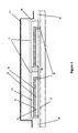
- an RPEC module consist of two RPEC elements (17) deposited on a substrate (18).
- the substrate (18) is covered by a Transparent Electron Conductor -TEC (19), electrically isolated in certain areas (20).
- Each of two the RPEC elements (17) contains a titanium dioxide (titania) layer (21), an insulating layer (22) and a catalytic conductor layer (23).
- the titania layer (21) is coated with a thin layer of a dye (24).
- Electrolyte (25) is added to the spaces within the porous titania-insulator-catalytic layers.
- a laminate formed by a polymeric layer (26) and a metal foil (27) is bonded to remaining patterned polymeric film (28) adhering to regions of the multiply-coated substrate (18).
Abstract
Description
- This invention relates to single cell and multi-cell regenerative photovoltaic photoelectrochemical (RPEC) devices, and to materials and methods used for manufacture of such devices.
- Examples of the RPEC cells of the type concerned are disclosed in the following US patterns:
-
4927721 , Photoelectrochemical cell; Michael Graetzel and Paul Liska, 1990. -
5350644 , Photovoltaic cells; Michael Graetzel, Mohammad K Nazeeruddin and Brian O'Regan, 1994. -
5525440 -
5728487 - RPEC cells, as of the type disclosed in the above patterns, are capable of being fabricated in a laminate arrangement between two large area substrates without undue expense. One typical arrangement involves two glass substrates, each utilising an electrically conducting coating upon the internal surface of the substrate. Another typical arrangement involves the first substrate being glass or polymeric and utilising an electrically conducting coating upon the internal surface of the substrate, with the second substrate being polymeric. In some arrangements, the internal surface of said second polymeric substrate is coated with an electrically conducting coating, whereas in other arrangements, said second polymeric substrate comprises a polymeric foil laminate, utilising adjacent electrically conductive material, such as carbon. Also, in some arrangements, the external surface may be a laminated metal film, and in other arrangements, the external surface may be coated by a metal. At least one of said first and second substrates is substantially transparent to visible light, as is the attached transparent electrically conducting (TEC) coating. RPEC cells contain a photoanode, typically comprising a ruthenium dye-sensitised, nanoporous semiconducting oxide (eg. titania) layer attached to one conductive coating, and a cathode, typically comprising a redox electrocatalyst layer attached to the other conductive coating or conductive material. An electrolyte containing a redox mediator is located between the photoanode and cathode, and the electrolyte is sealed from the environment. If one or more polymer substrates are utilised, the photoanode and the cathode are typically electrically separated by a porous insulating layer (eg. insulating ceramic oxides) or spacer(s) (eg. insulating spheres). TEC coatings, which usually comprise a metal oxide(s), have high resistivity when compared with normal metal conductors, resulting in high resistive losses for large area RPEC cells operating under high illumination. When operating under high illumination, one method to minimise these losses is the deposition of one or more networks of electrically conductive material that serve to collect and/or distribute electrons in the cell. Another method to minimise these losses is by connecting a multiple of RPEC cells (here called 'RPEC modules') in series to generate higher voltages and to minimise total current. Such connections in RPEC modules may be made externally or internally (International Application
PCT/AU00/00190 - One example of the manufacture of an RPEC module involves the use of two glass substrates that have TEC-coatings that have been divided into electrically isolated regions. Titanium dioxide (or similar semiconductor) is screen printed onto selected areas of the TEC coating of one substrate and an electrocatalyst is screen printed onto selected areas of the TEC coating of the other substrate. The titanium dioxide (titania) is coated with a thin layer of a dye by immersion of the titania-coated substrate in the dye solution. Strips of sealant and interconnect material are deposited upon one of the substrates and the two substrates are then bonded together. Electrolyte is added to the cells via access apertures in one of the substrates and these apertures are then sealed.
- Another example of the manufacture of an RPEC module involves the use of one substrate with a TEC-coating that has been divided into electrically isolated regions. Successive layers of titania, insulating ceramic oxide, and conducting catalytic material (for example, carbon-based) are deposited, for example by screen printing, onto selected areas of the TEC-coated substrate, with the catalytic layer also serving as an interconnect. The titania is coated with a thin layer of the dye by immersion of the multiple-coated substrate in the dye solution. Electrolyte is added to the spaces within the porous titania-insulator-catalytic layers. The sealant face of a sealant/polymer and/or metal foil laminate is sealed to the substrate.
- One of the difficulties in the manufacture of RPEC cells and modules is that when the semiconducting oxide-coated substrate is exposed to the dye solution, dye not only adsorbs to the semiconducting oxide, but also to the conductive coating. Similarly, if sealant has been applied to the semiconducting oxide-coated substrate, exposure to the dye solution typically results in dye adsorption to the sealant surface. The adsorbed dye on the conductive coating or sealant can interfere with the strength and/or permeability of any bond made to these surfaces during sealing, and also can affect the performance and service life of the RPEC cell. One process that prevents dye adsorption to the conductive coating involves covering relevant areas of the conducting coating with a polymeric film, application of dye to the coated substrate and then removal of the polymeric film, thus leaving a clean conductive coating surface to which a subsequent seal may be made. Another process that prevents dye adsorption to the conductive coating involves use of a laminated film (eg. surlyn/polypropylene) in which one face (eg. the surlyn face) is sealed to the relevant areas of the conducting coating, after which the dye is applied to the coated substrate and then the upper layer (eg. polypropylene) is removed, thus leaving a clean polymer (eg. surlyn) surface to which a subsequent seal may be made. This subsequent seal may involve additional sealant material or may involve sealing directly to the sealant surface, with the seal being made to a coated glass substrate or to a polymeric foil laminate, such as surlyn/aluminium. Unfortunately, these protective film processes are inconvenient and time consuming and can result in variability in performance of the RPEC. An additional impediment to a continuous manufacturing process is that dye application to the semiconducting oxide needs to be automated to be carried out efficiently, preferably within a low volume container that may be dark, heated, and provided with a partially sealed, low-oxygen content atmosphere.
- The present invention provides a method for manufacturing regenerative photoelectrochemical (RPEC) devices in a production line, each device being deposited on a substrate, the method comprising the steps of:
- dispensing a protective film in a substantially continuous sheet;
- attaching at least one substrate to the protective film in such a way that a predetermined areas of the substrate are protected from being coated during at least one subsequent manufacturing process;
- using the protective films as a means to transport the substrate, along the production line through the at least one subsequent manufacturing process.
- The protective film may comprise a patterned composite, laminated or multilayer film (CLM film) and the substrate may be a multiply-coated substrate of RPEC cells and modules. The protective film may be patterned to create apertures, which are used as engagement means and the step of transporting the substrate comprises penetrating the engagement means with teeth to locate and mechanically engage the film in transportation of the film/substrate composite..
- The method allows continuous and convenient transport of the CLM film/substrate composite, using the engagement means, through one or more steps of the manufacturing process, including, but not limited to application of dye to the semiconductor oxide, addition of electrolyte, continuous removal of part of said patterned CLM film and sealing of the multiply-coated substrate to another substrate. The patterned film has the advantage of preventing adsorption of dye on the predetermined areas of said substrate. A portion of the part of said patterned film not removed may be utilised as sealant to subsequently bond the substrates of the RPEC cells and modules.
- In one embodiment, the present invention provides for application of a continuous patterned CLM film to a multiply-coated substrate of RPEC cells and modules, and continuous and convenient transport of the patterned film/substrate composite through one or more steps of the manufacturing process, including, but not limited to application of dye to the semiconductor oxide, addition of electrolyte, continuous removal of part of said patterned CLM film and sealing of the multiply-coated substrate to another substrate.
- The patterned film may be a laminate of two or more polymers plus the option of an external layer of metallic or other materials, whereby one of the external layers of the laminate will function as the sealant of the RPEC device. The other layer(s) of the laminate function to prevent access of the dye, electrolyte, solvents and/or other materials to one face of the sealant layer. The patterned film may be dispensed in a substantially continuous sheet, preferably from a roll, and may be continuously patterned using stamping, rolling or any of the known methods of such patterning, to remove portions of film, thereby leaving apertures, hereby termed access regions, and optionally also leaving other apertures, hereby termed engagement means. If desired, a sealant face of said patterned film and/or predetermined areas of the surface of the multiply-coated substrate are treated with an adhesion promoting means, such as an adhesion primer, corona discharge or other known processes, in order to effect superior adhesion of said treated face and/or said treated surface in the subsequent bonding process. The substrate may be bonded to said patterned film by using roller, hot roller, stamping, or hot stamping processes, or by any of the known methods of such bonding. Particular care must be taken in the bonding process to ensure desired alignment of multiply-coated areas of said substrates with said access regions of said patterned film. Said access regions enable access to at least one selected area of said substrate, by dye solutions, electrolyte, solvents, gases and such like materials in subsequent steps of said continuous manufacturing process. Mechanical contact is made with said patterned film in order to transport said patterned film attached to the substrate i.e. the "film/substrate composite", through subsequent steps of said continuous manufacturing process. Said mechanical contact may comprise any of the known methods of mechanical contact used to transport a film. Said mechanical contact includes, but is not limited to penetration of said engagement means by projections that are then moved to effect said transport, whereby said projections include, but are not limited to teeth of sprockets, teeth in linear placement as in racks, hooks, supports and such like mechanical devices as are known to those of ordinary skill in the art. Said sprockets may be round, or essentially triangular, square, polygonal or of any suitable shape, and the apertures comprising the engagement means may be square, round or of any suitable shape, and may form one or more lines along the length of said patterned film. Said mechanical contact may include, but is not limited to opposing sets of rollers touching said film that passes between said sets of rollers, and with first set of rollers moved in opposite rotation to second set of rollers in order to transport said film in the desired direction. Said patterned film/substrate composite may be transported through a dye application chamber that may be dark, heated, and provided with a partially sealed, low-oxygen content atmosphere. Within said dye application chamber, said patterned film/substrate composite may be transported through the dye solution in a zig-zag manner, linearly, or in any other manner to provide effective use of the solution and space. Said dye solution may be agitated, such as by bubbles, stirring, pumping, ultrasonics or other known means of agitation. Said patterned film/substrate composite may be transported through a rinsing chamber, an electrolyte chamber, and other chambers, including but not limited to drying chambers. Part of said patterned film may then be removed in a continuous process, leaving the sealant layer of the patterned film adhering to regions of said multiply-coated substrate. Said mechanical contact with said sealant layer film enables convenient transport of said sealant film/substrate composite through subsequent steps of said continuous manufacturing process, including sealing of exposed surface of clean sealant on said multiply-coated substrate to a second substrate. Said multiply-coated substrate may comprise a TEC-coated glass substrate or a polymeric substrate, upon which subsequent layers of material are deposited. Said second substrate may comprise a TEC-coated glass substrate, a polymeric substrate, or a polymeric/metal foil laminate, such as surlyn/aluminium, whereby part of the polymeric layer (eg. surlyn) of said polymeric/metal foil laminate (eg. surlyn/aluminium) is bonded to said remaining patterned polymeric film (eg. surlyn) that is adhering to regions of the multiply-coated substrate. If used, polymeric substrates and polymeric/metal foil laminates, may be dispensed in a substantially continuous sheet, preferably from a roll.
- Throughout this specification, unless the context requires otherwise, the word "comprise" or variations such as "comprises" or "comprising", will be understood to imply the inclusion of a stated element or integer or group of elements or integers but not the exclusion of any other element or integer or group of elements or integers.
- Having broadly portrayed the nature of the present invention, embodiments thereof will now be described by way of example and illustration only. In the following description, reference will be made to the accompanying drawings in which:
-
Figure 1 is a diagrammatic representation of a continuous process for manufacturing RPEC cells and modules in accordance with the chosen example of the invention. -
Figure 2 is a diagrammatic representation of a patterned CLM film in accordance with the chosen example of the invention. -
Figure 3 is a diagrammatic representation of a patterned CLM film/substrate composite being transported through a dyeing chamber in a zig-zag manner in accordance with the chosen example of the invention. -
Figure 4 is a diagrammatic representation of example of an RPEC module based on 1 glass substrate in accordance with the chosen example of invention - Referring to
Figure 1 , a CLM film (1a) is dispensed from a roll (1b) and is subjected to a patterning process (2) whereby portions of film are removed, leaving a patterned CLM film (1c) with access regions (1d) and engagement means in the form of apertures (1e), as shown inFigure 2 . The patterned CLM film (1a) is then treated with adhesion promoters (3) as are selected areas of the surfaces of the multiply-coated glass substrates (3). The multiply-coated substrates are then bonded (4,5) to the continuous patterned CLM film (1a), ensuring desired alignment of multiply-coated areas of the substrates with the access regions of the patterned CLM film. The patterned CLM film/substrate composite is then transported through subsequent steps of the continuous manufacturing process by mechanical contact of sprocket teeth with the engagement means of the patterned CLM film. The patterned CLM film/substrate composite is then transported through a low volume dyeing chamber (6) that is dark, heated, and provided with a partially sealed, low-oxygen content atmosphere. Within the dyeing chamber, the patterned CLM film/substrate composite is transported through a stirred dye solution in a zig-zag manner as shown inFigure 3 . The patterned CLM film/substrate composite is then transported through a chamber (7) where the composite is rinsed, dried and exposed to electrolyte solution. The upper layer of the patterned CLM film (1c) is then peeled from the CLM film/substrate composite in a continuous process (8), and collected upon a roller (9), leaving exposed the upper surface of the sealant layer of the patterned sealant film/substrate composite. The patterned sealant film/substrate composite is then transported through subsequent steps of the continuous manufacturing process by mechanical contact of sprocket teeth with the engagement means of the patterned sealant film. The sealant surface of a sealant/metal foil laminate is dispensed from a roll (not shown) and then sealed (11) to the exposed surface of clean sealant on the patterned sealant film/substrate composite. - Referring to
Figure 2 , the access regions (1d) (rectangles) and engagement means (1e) (circles) of a patterned CLM film (1c) are shown as viewed from the direction of thearrow 14 inFigure 1 . - Referring to
Figure 3 , a patterned CLM film/substrate composite 15 is shown being transported through a dyeing chamber in a zig-zag manner. - Referring to
Figure 4 , an RPEC module consist of two RPEC elements (17) deposited on a substrate (18). The substrate (18) is covered by a Transparent Electron Conductor -TEC (19), electrically isolated in certain areas (20). Each of two the RPEC elements (17) contains a titanium dioxide (titania) layer (21), an insulating layer (22) and a catalytic conductor layer (23). The titania layer (21) is coated with a thin layer of a dye (24). Electrolyte (25) is added to the spaces within the porous titania-insulator-catalytic layers. A laminate formed by a polymeric layer (26) and a metal foil (27) is bonded to remaining patterned polymeric film (28) adhering to regions of the multiply-coated substrate (18).
Claims (22)
- A method for manufacturing regenerative photoelectrochemical (RPEC) devices in a production line, each device being deposited on a substrate, the method comprising the steps of:- dispensing a protective film in a substantially continuous sheet;- attaching at least one substrate to the protective film in such a way that a predetermined areas of the substrate are protected from being coated during at least one subsequent manufacturing process;- using the protective films as a means to transport the substrate, along the production line through the at least one subsequent manufacturing process.
- The method according to claim 1, wherein the method comprises a step of coating the substrate with one or more device layers on at least one selected area of the substrate not overlapping with the predetermined area.
- The method according to claim 2 wherein at least one of the device layers comprises a layer of porous large band gap semiconducting oxide.
- The method according to claim 2, wherein the one or more device layers comprise porous layers of:- large band gap semiconducting oxide;- insulating ceramic oxide; and- a conducting catalytic layer.
- The method of according to either claim 3 or claim 4 wherein the one or more manufacturing processes comprises the following steps:- applying a thin layer of dye to said porous large band gap semiconducting oxide layer;- adding electrolyte to spaces within the layers;- sealing the device by applying a sealant over the whole substrate, wherein a layer of the patterned film is arranged to bond to the sealant over the predetermined area.
- The method according to any one of the preceding claims, wherein the protective film is dispensed to the production line from a roll.
- The method according to any one of the preceding claims wherein the protective film is continuously patterned by removing portions of the film such that apertures are created, wherein at least some of apertures comprise access regions which define the at least one selected area of the substrate.
- The method according to any one of the preceding claims wherein the protective film is continuously patterned by removing portions of the film such that apertures are created, wherein at least some of apertures comprise the engagement means, and the step of transporting the substrate comprises penetrating the engagement means with teeth to locate and mechanically engage the film to assist transportation through the one or more manufacturing processes.
- The method according to any one of the preceding claims wherein one face of the protective film is continuously treated with an adhesion promoting means for improving adhesion of the treated face to the substrate.
- The method according to any one of the preceding claims wherein the predetermined area of the substrate is continuously treated with an adhesion promoting means for improving adhesion of the predetermined area to the patterned film.
- The method according to any one of the preceding claims wherein the film is bonded to the predetermined area of the substrate using a roller, hot roller, stamping, or hot stamping.
- The method according to any one of the preceding claims wherein the substrate attached to the protective film is transported through a dyeing chamber.
- The method according to claim 12 wherein the substrate is transported with the protective film through the dyeing chamber in a zigzag or reciprocating manner to provide effect use of dye and chamber space.
- The method according to claim 13 wherein a dye solution in the dyeing chamber is agitated.
- The method according to any one of the preceding claims wherein the protective film is a composite, laminated or multilayer (CLM) film in which a first layer arranged to be adjacent to the substrate is a sealant layer, and a second layer is a protective layer.
- The method according to claim 15, wherein the second layer of the CLM film is removed in a continuous process, leaving the sealant layer adhering to the predetermined area of the substrate.
- The method according to claim 16 wherein the sealant layer is used to transport the substrate through subsequent manufacturing processes, including sealing of the sealant layer to a second substrate.
- The method according to claim 17 wherein the second substrate comprises a TEC-coated glass substrate.
- The method according to claim 17 wherein the second substrate comprises a polymeric substrate.
- The method according to claim 17 wherein the second substrate comprises a polymeric/metal foil or polymeric/metal/polymeric laminate whereby part of first polymeric layer in the laminate is arranged to bond to a polymeric layer attached to the predetermined area of the substrate.
- The method according to either claim 19 or 20 wherein the second substrate is dispensed in a substantially continuous sheet.
- The method according to claim 21 wherein the second substrate is dispensed from a roll.
Applications Claiming Priority (3)
| Application Number | Priority Date | Filing Date | Title |
|---|---|---|---|
| AUPP953999 | 1999-03-30 | ||
| AUPP9539A AUPP953999A0 (en) | 1999-03-30 | 1999-03-30 | Methods to manufacture single cell and multi-cell regenerative photoelectrochemical devices |
| PCT/AU2000/000274 WO2000059816A1 (en) | 1999-03-30 | 2000-03-30 | Methods to manufacture single cell and multi-cell regenerative photoelectrochemical devices |
Publications (3)
| Publication Number | Publication Date |
|---|---|
| EP1200325A1 EP1200325A1 (en) | 2002-05-02 |
| EP1200325A4 EP1200325A4 (en) | 2008-12-03 |
| EP1200325B1 true EP1200325B1 (en) | 2009-12-16 |
Family
ID=3813736
Family Applications (1)
| Application Number | Title | Priority Date | Filing Date |
|---|---|---|---|
| EP00912270A Expired - Lifetime EP1200325B1 (en) | 1999-03-30 | 2000-03-30 | Methods to manufacture single cell and multi-cell regenerative photoelectrochemical devices |
Country Status (9)
| Country | Link |
|---|---|
| US (1) | US6652904B1 (en) |
| EP (1) | EP1200325B1 (en) |
| AT (1) | ATE452087T1 (en) |
| AU (1) | AUPP953999A0 (en) |
| DE (1) | DE60043543D1 (en) |
| DK (1) | DK1200325T3 (en) |
| ES (1) | ES2336299T3 (en) |
| PT (1) | PT1200325E (en) |
| WO (1) | WO2000059816A1 (en) |
Families Citing this family (14)
| Publication number | Priority date | Publication date | Assignee | Title |
|---|---|---|---|---|
| AUPP931799A0 (en) * | 1999-03-18 | 1999-04-15 | Sustainable Technologies Australia Limited | Methods to implement interconnects in multi-cell regenerative photovoltaic photoelectrochemical devices |
| SE521683C2 (en) * | 2000-06-14 | 2003-11-25 | Ivf Industriforskning Och Utve | Method of Manufacture of Sealed Monolithic Electrochemical Systems and Sealed Monolithic Electrochemical System |
| AUPR099500A0 (en) * | 2000-10-25 | 2000-11-16 | Sustainable Technologies International Pty Ltd | Uv sensors and arrays and methods to manufacture thereof |
| WO2004036683A1 (en) * | 2002-10-15 | 2004-04-29 | Sharp Kabushiki Kaisha | Sensitized dye solar cell and sensitized dye solar cell module |
| JP2004342755A (en) * | 2003-05-14 | 2004-12-02 | Shinko Electric Ind Co Ltd | Method of manufacturing plane coil |
| JP5219373B2 (en) * | 2003-11-03 | 2013-06-26 | ダイソル・インダストリーズ・プロプライエタリー・リミテッド | Multilayer photovoltaic device on the coating surface |
| US20060243587A1 (en) * | 2004-05-05 | 2006-11-02 | Sustainable Technologies International Pty Ltd | Photoelectrochemical device |
| CN1969350B (en) * | 2004-06-15 | 2010-06-16 | 戴索有限公司 | Photovoltaic module with full utilization of surface area |
| JP4063802B2 (en) * | 2004-08-04 | 2008-03-19 | シャープ株式会社 | Photoelectrode |
| US7820022B2 (en) * | 2005-11-28 | 2010-10-26 | General Electric Company | Photoelectrochemical cell and method of manufacture |
| US8933328B2 (en) * | 2006-07-06 | 2015-01-13 | Sharp Kabushiki Kaisha | Dye-sensitized solar cell module and method of producing the same |
| WO2008093113A2 (en) * | 2007-02-02 | 2008-08-07 | G24 Innovations Limited | A method of manufacturing an electrode array for photovoltaic electrochemical cell arrays |
| JP2009146625A (en) * | 2007-12-12 | 2009-07-02 | Sony Corp | Dye-sensitized photoelectric conversion element module, manufacturing method thereof, photoelectric conversion element module, and manufacturing method thereof, as well as electronic apparatus |
| DE102018132342A1 (en) * | 2018-12-14 | 2020-06-18 | Heliatek Gmbh | Stabilization of laser structured organic photovoltaics |
Family Cites Families (12)
| Publication number | Priority date | Publication date | Assignee | Title |
|---|---|---|---|---|
| US4133697A (en) * | 1977-06-24 | 1979-01-09 | Nasa | Solar array strip and a method for forming the same |
| EP0066339A2 (en) | 1981-05-22 | 1982-12-08 | North American Philips Corporation | Polyfoam chip carrier tape |
| CA1309510C (en) * | 1989-09-29 | 1992-10-27 | Vincent Scarnecchia | Carrier continuous film for heat fusible materials |
| JPH0469618A (en) * | 1990-07-10 | 1992-03-04 | Sharp Corp | Manufacture of liquid crystal display device |
| US5273608A (en) * | 1990-11-29 | 1993-12-28 | United Solar Systems Corporation | Method of encapsulating a photovoltaic device |
| US5328546A (en) | 1992-04-03 | 1994-07-12 | International Business Machines Corp. | Photo resist film application mechanism |
| TW283819B (en) * | 1995-02-03 | 1996-08-21 | Fuji Photo Film Co Ltd | |
| US5735966A (en) * | 1995-05-15 | 1998-04-07 | Luch; Daniel | Substrate structures for integrated series connected photovoltaic arrays and process of manufacture of such arrays |
| JP3061354B2 (en) * | 1995-05-23 | 2000-07-10 | ソマール株式会社 | Film sticking method and apparatus |
| AU728725B2 (en) * | 1995-10-31 | 2001-01-18 | Ecole Polytechnique Federale De Lausanne | A battery of photovoltaic cells and process for manufacturing the same |
| JP2001085076A (en) * | 1999-09-10 | 2001-03-30 | Fuji Photo Film Co Ltd | Photoelectric transducer and photocell |
| JP4414036B2 (en) * | 1999-12-27 | 2010-02-10 | シャープ株式会社 | Method for producing dye-sensitized solar cell |
-
1999
- 1999-03-30 AU AUPP9539A patent/AUPP953999A0/en not_active Abandoned
-
2000
- 2000-03-30 WO PCT/AU2000/000274 patent/WO2000059816A1/en active IP Right Grant
- 2000-03-30 US US09/980,268 patent/US6652904B1/en not_active Expired - Fee Related
- 2000-03-30 AT AT00912270T patent/ATE452087T1/en not_active IP Right Cessation
- 2000-03-30 DE DE60043543T patent/DE60043543D1/en not_active Expired - Lifetime
- 2000-03-30 EP EP00912270A patent/EP1200325B1/en not_active Expired - Lifetime
- 2000-03-30 DK DK00912270.6T patent/DK1200325T3/en active
- 2000-03-30 PT PT00912270T patent/PT1200325E/en unknown
- 2000-03-30 ES ES00912270T patent/ES2336299T3/en not_active Expired - Lifetime
Also Published As
| Publication number | Publication date |
|---|---|
| ATE452087T1 (en) | 2010-01-15 |
| EP1200325A1 (en) | 2002-05-02 |
| PT1200325E (en) | 2010-03-17 |
| AUPP953999A0 (en) | 1999-04-29 |
| EP1200325A4 (en) | 2008-12-03 |
| ES2336299T3 (en) | 2010-04-12 |
| US6652904B1 (en) | 2003-11-25 |
| WO2000059816A1 (en) | 2000-10-12 |
| DE60043543D1 (en) | 2010-01-28 |
| DK1200325T3 (en) | 2010-04-26 |
Similar Documents
| Publication | Publication Date | Title |
|---|---|---|
| US9704653B2 (en) | Photovoltaic cell | |
| EP0858669B1 (en) | A battery of photovoltaic cells and process for manufacturing the same | |
| EP1200325B1 (en) | Methods to manufacture single cell and multi-cell regenerative photoelectrochemical devices | |
| AU741400B2 (en) | Method for making a photovoltaic cell containing a dye | |
| JPH11514787A (en) | Photovoltaic cell battery and method of manufacturing the same | |
| US6555741B1 (en) | Methods to implement interconnects in multi-cell regenerative photovoltaic photoelectrochemical devices | |
| JP2004119306A (en) | Photoelectric conversion element and its manufacturing method | |
| JP2001160426A (en) | Dye-sensitization type solar battery, its manufacturing method and portable equipment using the same | |
| JP5086520B2 (en) | Photoelectric conversion element module | |
| AU767569B2 (en) | Methods to manufacture single cell and multi-cell regenerative photoelectrochemical devices | |
| WO2010042170A2 (en) | Interconnection of adjacent devices | |
| CN105453203B (en) | Plastic solar dye cell | |
| US20100307581A1 (en) | Large area dye cells, and methods of production thereof | |
| WO1998005084A1 (en) | Photoelectrochemical cell | |
| AU761370B2 (en) | Methods to implement interconnects in multi-cell regenerative photovoltaic photoelectrochemical devices | |
| EP2359406A1 (en) | Photovoltaic devices | |
| JP2013201078A (en) | Electric module and manufacturing method of the same | |
| KR20190062436A (en) | Dye-sensitized solar cell module |
Legal Events
| Date | Code | Title | Description |
|---|---|---|---|
| PUAI | Public reference made under article 153(3) epc to a published international application that has entered the european phase |
Free format text: ORIGINAL CODE: 0009012 |
|
| 17P | Request for examination filed |
Effective date: 20011026 |
|
| AK | Designated contracting states |
Kind code of ref document: A1 Designated state(s): AT BE CH CY DE DK ES FI FR GB GR IE IT LI LU MC NL PT SE |
|
| AX | Request for extension of the european patent |
Free format text: AL;LT;LV;MK;RO;SI |
|
| RAP1 | Party data changed (applicant data changed or rights of an application transferred) |
Owner name: DYESOL LTD |
|
| A4 | Supplementary search report drawn up and despatched |
Effective date: 20081105 |
|
| RIC1 | Information provided on ipc code assigned before grant |
Ipc: B65G 49/06 20060101AFI20001018BHEP Ipc: C03C 17/00 20060101ALI20081030BHEP Ipc: C03C 17/25 20060101ALI20081030BHEP Ipc: G02B 1/11 20060101ALI20081030BHEP Ipc: B65G 35/04 20060101ALI20081030BHEP Ipc: C03C 3/12 20060101ALI20081030BHEP Ipc: H01G 9/20 20060101ALI20081030BHEP Ipc: H01M 6/36 20060101ALI20081030BHEP |
|
| GRAP | Despatch of communication of intention to grant a patent |
Free format text: ORIGINAL CODE: EPIDOSNIGR1 |
|
| GRAS | Grant fee paid |
Free format text: ORIGINAL CODE: EPIDOSNIGR3 |
|
| GRAA | (expected) grant |
Free format text: ORIGINAL CODE: 0009210 |
|
| AK | Designated contracting states |
Kind code of ref document: B1 Designated state(s): AT BE CH CY DE DK ES FI FR GB GR IE IT LI LU MC NL PT SE |
|
| REG | Reference to a national code |
Ref country code: GB Ref legal event code: FG4D |
|
| REG | Reference to a national code |
Ref country code: CH Ref legal event code: EP |
|
| REG | Reference to a national code |
Ref country code: IE Ref legal event code: FG4D |
|
| REF | Corresponds to: |
Ref document number: 60043543 Country of ref document: DE Date of ref document: 20100128 Kind code of ref document: P |
|
| REG | Reference to a national code |
Ref country code: SE Ref legal event code: TRGR |
|
| REG | Reference to a national code |
Ref country code: PT Ref legal event code: SC4A Free format text: AVAILABILITY OF NATIONAL TRANSLATION Effective date: 20100311 |
|
| REG | Reference to a national code |
Ref country code: GR Ref legal event code: EP Ref document number: 20100400486 Country of ref document: GR |
|
| REG | Reference to a national code |
Ref country code: NL Ref legal event code: T3 |
|
| REG | Reference to a national code |
Ref country code: ES Ref legal event code: FG2A Ref document number: 2336299 Country of ref document: ES Kind code of ref document: T3 |
|
| REG | Reference to a national code |
Ref country code: DK Ref legal event code: T3 |
|
| PG25 | Lapsed in a contracting state [announced via postgrant information from national office to epo] |
Ref country code: FI Free format text: LAPSE BECAUSE OF FAILURE TO SUBMIT A TRANSLATION OF THE DESCRIPTION OR TO PAY THE FEE WITHIN THE PRESCRIBED TIME-LIMIT Effective date: 20091216 |
|
| PG25 | Lapsed in a contracting state [announced via postgrant information from national office to epo] |
Ref country code: AT Free format text: LAPSE BECAUSE OF FAILURE TO SUBMIT A TRANSLATION OF THE DESCRIPTION OR TO PAY THE FEE WITHIN THE PRESCRIBED TIME-LIMIT Effective date: 20091216 |
|
| PLBE | No opposition filed within time limit |
Free format text: ORIGINAL CODE: 0009261 |
|
| STAA | Information on the status of an ep patent application or granted ep patent |
Free format text: STATUS: NO OPPOSITION FILED WITHIN TIME LIMIT |
|
| PG25 | Lapsed in a contracting state [announced via postgrant information from national office to epo] |
Ref country code: CY Free format text: LAPSE BECAUSE OF FAILURE TO SUBMIT A TRANSLATION OF THE DESCRIPTION OR TO PAY THE FEE WITHIN THE PRESCRIBED TIME-LIMIT Effective date: 20091216 Ref country code: MC Free format text: LAPSE BECAUSE OF NON-PAYMENT OF DUE FEES Effective date: 20100331 |
|
| 26N | No opposition filed |
Effective date: 20100917 |
|
| PGFP | Annual fee paid to national office [announced via postgrant information from national office to epo] |
Ref country code: ES Payment date: 20110425 Year of fee payment: 12 Ref country code: BE Payment date: 20110324 Year of fee payment: 12 |
|
| PGFP | Annual fee paid to national office [announced via postgrant information from national office to epo] |
Ref country code: IE Payment date: 20120125 Year of fee payment: 13 |
|
| PGFP | Annual fee paid to national office [announced via postgrant information from national office to epo] |
Ref country code: PT Payment date: 20120309 Year of fee payment: 13 |
|
| PGFP | Annual fee paid to national office [announced via postgrant information from national office to epo] |
Ref country code: DK Payment date: 20120323 Year of fee payment: 13 |
|
| PG25 | Lapsed in a contracting state [announced via postgrant information from national office to epo] |
Ref country code: LU Free format text: LAPSE BECAUSE OF NON-PAYMENT OF DUE FEES Effective date: 20100330 |
|
| BERE | Be: lapsed |
Owner name: DYESOL LTD Effective date: 20120331 |
|
| PG25 | Lapsed in a contracting state [announced via postgrant information from national office to epo] |
Ref country code: BE Free format text: LAPSE BECAUSE OF NON-PAYMENT OF DUE FEES Effective date: 20120331 |
|
| PGFP | Annual fee paid to national office [announced via postgrant information from national office to epo] |
Ref country code: NL Payment date: 20130221 Year of fee payment: 14 |
|
| REG | Reference to a national code |
Ref country code: ES Ref legal event code: FD2A Effective date: 20130710 |
|
| PG25 | Lapsed in a contracting state [announced via postgrant information from national office to epo] |
Ref country code: ES Free format text: LAPSE BECAUSE OF NON-PAYMENT OF DUE FEES Effective date: 20120331 |
|
| REG | Reference to a national code |
Ref country code: PT Ref legal event code: MM4A Free format text: LAPSE DUE TO NON-PAYMENT OF FEES Effective date: 20130930 |
|
| REG | Reference to a national code |
Ref country code: DK Ref legal event code: EBP Effective date: 20130331 |
|
| PG25 | Lapsed in a contracting state [announced via postgrant information from national office to epo] |
Ref country code: PT Free format text: LAPSE BECAUSE OF NON-PAYMENT OF DUE FEES Effective date: 20130930 |
|
| REG | Reference to a national code |
Ref country code: IE Ref legal event code: MM4A |
|
| PG25 | Lapsed in a contracting state [announced via postgrant information from national office to epo] |
Ref country code: IE Free format text: LAPSE BECAUSE OF NON-PAYMENT OF DUE FEES Effective date: 20130330 |
|
| PG25 | Lapsed in a contracting state [announced via postgrant information from national office to epo] |
Ref country code: DK Free format text: LAPSE BECAUSE OF NON-PAYMENT OF DUE FEES Effective date: 20130331 |
|
| PGFP | Annual fee paid to national office [announced via postgrant information from national office to epo] |
Ref country code: CH Payment date: 20140326 Year of fee payment: 15 Ref country code: SE Payment date: 20140320 Year of fee payment: 15 |
|
| PGFP | Annual fee paid to national office [announced via postgrant information from national office to epo] |
Ref country code: GR Payment date: 20140228 Year of fee payment: 15 Ref country code: IT Payment date: 20140326 Year of fee payment: 15 |
|
| PGFP | Annual fee paid to national office [announced via postgrant information from national office to epo] |
Ref country code: GB Payment date: 20140224 Year of fee payment: 15 |
|
| PGFP | Annual fee paid to national office [announced via postgrant information from national office to epo] |
Ref country code: FR Payment date: 20140324 Year of fee payment: 15 Ref country code: DE Payment date: 20140530 Year of fee payment: 15 |
|
| REG | Reference to a national code |
Ref country code: NL Ref legal event code: V1 Effective date: 20141001 |
|
| PG25 | Lapsed in a contracting state [announced via postgrant information from national office to epo] |
Ref country code: NL Free format text: LAPSE BECAUSE OF NON-PAYMENT OF DUE FEES Effective date: 20141001 |
|
| REG | Reference to a national code |
Ref country code: DE Ref legal event code: R119 Ref document number: 60043543 Country of ref document: DE |
|
| REG | Reference to a national code |
Ref country code: CH Ref legal event code: PL |
|
| GBPC | Gb: european patent ceased through non-payment of renewal fee |
Effective date: 20150330 |
|
| PG25 | Lapsed in a contracting state [announced via postgrant information from national office to epo] |
Ref country code: SE Free format text: LAPSE BECAUSE OF NON-PAYMENT OF DUE FEES Effective date: 20150331 |
|
| REG | Reference to a national code |
Ref country code: SE Ref legal event code: EUG |
|
| REG | Reference to a national code |
Ref country code: GR Ref legal event code: ML Ref document number: 20100400486 Country of ref document: GR Effective date: 20151002 |
|
| PG25 | Lapsed in a contracting state [announced via postgrant information from national office to epo] |
Ref country code: IT Free format text: LAPSE BECAUSE OF NON-PAYMENT OF DUE FEES Effective date: 20150330 |
|
| REG | Reference to a national code |
Ref country code: FR Ref legal event code: ST Effective date: 20151130 |
|
| PG25 | Lapsed in a contracting state [announced via postgrant information from national office to epo] |
Ref country code: CH Free format text: LAPSE BECAUSE OF NON-PAYMENT OF DUE FEES Effective date: 20150331 Ref country code: LI Free format text: LAPSE BECAUSE OF NON-PAYMENT OF DUE FEES Effective date: 20150331 Ref country code: GR Free format text: LAPSE BECAUSE OF NON-PAYMENT OF DUE FEES Effective date: 20151002 Ref country code: GB Free format text: LAPSE BECAUSE OF NON-PAYMENT OF DUE FEES Effective date: 20150330 Ref country code: DE Free format text: LAPSE BECAUSE OF NON-PAYMENT OF DUE FEES Effective date: 20151001 |
|
| PG25 | Lapsed in a contracting state [announced via postgrant information from national office to epo] |
Ref country code: FR Free format text: LAPSE BECAUSE OF NON-PAYMENT OF DUE FEES Effective date: 20150331 |