EP1199837A2 - Sampling clock generation circuit, data transfer control device, and electronic equipment - Google Patents
Sampling clock generation circuit, data transfer control device, and electronic equipment Download PDFInfo
- Publication number
- EP1199837A2 EP1199837A2 EP01124703A EP01124703A EP1199837A2 EP 1199837 A2 EP1199837 A2 EP 1199837A2 EP 01124703 A EP01124703 A EP 01124703A EP 01124703 A EP01124703 A EP 01124703A EP 1199837 A2 EP1199837 A2 EP 1199837A2
- Authority
- EP
- European Patent Office
- Prior art keywords
- clock
- circuit
- data
- clocks
- sampling clock
- Prior art date
- Legal status (The legal status is an assumption and is not a legal conclusion. Google has not performed a legal analysis and makes no representation as to the accuracy of the status listed.)
- Granted
Links
Images









Classifications
-
- G—PHYSICS
- G06—COMPUTING OR CALCULATING; COUNTING
- G06F—ELECTRIC DIGITAL DATA PROCESSING
- G06F1/00—Details not covered by groups G06F3/00 - G06F13/00 and G06F21/00
- G06F1/04—Generating or distributing clock signals or signals derived directly therefrom
- G06F1/06—Clock generators producing several clock signals
-
- G—PHYSICS
- G06—COMPUTING OR CALCULATING; COUNTING
- G06F—ELECTRIC DIGITAL DATA PROCESSING
- G06F13/00—Interconnection of, or transfer of information or other signals between, memories, input/output devices or central processing units
-
- H—ELECTRICITY
- H03—ELECTRONIC CIRCUITRY
- H03K—PULSE TECHNIQUE
- H03K3/00—Circuits for generating electric pulses; Monostable, bistable or multistable circuits
- H03K3/02—Generators characterised by the type of circuit or by the means used for producing pulses
- H03K3/027—Generators characterised by the type of circuit or by the means used for producing pulses by the use of logic circuits, with internal or external positive feedback
- H03K3/03—Astable circuits
- H03K3/0315—Ring oscillators
- H03K3/0322—Ring oscillators with differential cells
-
- H—ELECTRICITY
- H03—ELECTRONIC CIRCUITRY
- H03L—AUTOMATIC CONTROL, STARTING, SYNCHRONISATION OR STABILISATION OF GENERATORS OF ELECTRONIC OSCILLATIONS OR PULSES
- H03L7/00—Automatic control of frequency or phase; Synchronisation
- H03L7/06—Automatic control of frequency or phase; Synchronisation using a reference signal applied to a frequency- or phase-locked loop
- H03L7/08—Details of the phase-locked loop
- H03L7/099—Details of the phase-locked loop concerning mainly the controlled oscillator of the loop
- H03L7/0995—Details of the phase-locked loop concerning mainly the controlled oscillator of the loop the oscillator comprising a ring oscillator
- H03L7/0996—Selecting a signal among the plurality of phase-shifted signals produced by the ring oscillator
-
- H—ELECTRICITY
- H03—ELECTRONIC CIRCUITRY
- H03L—AUTOMATIC CONTROL, STARTING, SYNCHRONISATION OR STABILISATION OF GENERATORS OF ELECTRONIC OSCILLATIONS OR PULSES
- H03L7/00—Automatic control of frequency or phase; Synchronisation
- H03L7/06—Automatic control of frequency or phase; Synchronisation using a reference signal applied to a frequency- or phase-locked loop
- H03L7/16—Indirect frequency synthesis, i.e. generating a desired one of a number of predetermined frequencies using a frequency- or phase-locked loop
- H03L7/18—Indirect frequency synthesis, i.e. generating a desired one of a number of predetermined frequencies using a frequency- or phase-locked loop using a frequency divider or counter in the loop
-
- H—ELECTRICITY
- H04—ELECTRIC COMMUNICATION TECHNIQUE
- H04L—TRANSMISSION OF DIGITAL INFORMATION, e.g. TELEGRAPHIC COMMUNICATION
- H04L7/00—Arrangements for synchronising receiver with transmitter
- H04L7/02—Speed or phase control by the received code signals, the signals containing no special synchronisation information
- H04L7/033—Speed or phase control by the received code signals, the signals containing no special synchronisation information using the transitions of the received signal to control the phase of the synchronising-signal-generating means, e.g. using a phase-locked loop
- H04L7/0337—Selecting between two or more discretely delayed clocks or selecting between two or more discretely delayed received code signals
Definitions
- the present invention relates to a sampling clock generation circuit, a data transfer control device, and electronic equipment.
- USB Universal Serial Bus
- this USB standard In comparison with the IEEE 1394 standard that is attracting so much attention as a standard for the same serial bus interface, this USB standard has a problem in that the transfer speed thereof is slower.
- USB 2.0 transceiver macrocell interface which defined interface specifications for the physical-layer and logical-layer circuitry under USB 2.0, has also been decided upon.
- a data transfer control device connected to USB must generate a high-frequency sampling clock at 480 MHz, in order to sample the data that is transferred thereinto at 480 Mbps. It is also necessary to generate a sampling clock that makes it possible to ensure set-up and hold times during the data sampling. It is therefore extremely difficult to design such a sampling clock generation circuit.
- sampling clock generation circuit It would be possible in this case to implement such a sampling clock generation circuit by using the latest semiconductor processes which enable microprocessing, but it would be extremely difficult to implement a sampling clock generation circuit that is capable of such fast operation if up-to-date semiconductor processing cannot be used.
- One method of implementing a fast sampling clock generation circuit without employing the latest semiconductor processes is a method whereby the circuitry is laid out manually, clock skew is minimized, and synchronization is ensured.
- the present invention was devised in the light of the above described technical problems, making it possible to provide a sampling clock generation circuit that ensures sufficient times such as set-up times during sampling, while operating at a high frequency, together with a data transfer control device and electronic equipment that uses the same.
- the present invention relates to a sampling clock generation circuit which generates a sampling clock used for sampling data, the sampling clock generation circuit comprising:
- the present invention makes it possible to detect whether there is a data edge between any edges among the edges of first to N-th multi-phase clocks. It is thus possible to detect whether the data edge is between the first and second clocks or between the second and third clocks, by way of example.
- One clock of the first to N-th clocks is then selected, based on the thus-obtained edge detection information (information indicating there is a data edge between any edges of two clocks), and that clock is output as the sampling clock.
- the present invention makes it possible to generate a data sampling clock with a simple configuration whereby the selection of a clock from among the first to N-th clocks is based on edge detection information. It therefore makes it possible to generate a sampling clock that is suitable for sampling data (even data that is input in synchronization with a fast clock), using a compact circuit configuration.
- the edge detection circuit may comprise:
- This configuration makes it possible to detect whether there is a data edge between edges of any specific clocks, with a simple configuration in which only first to N-th holding circuits and first to N-th detection circuits are provided.
- number of clocks N of the first to N-th clocks may be such that: N ⁇ [T/(TS + TH)] (where [X] is a maximum integer that does not exceed X).
- This configuration makes it possible to obtain suitable edge detection information, even when the data held in the first to N-th holding circuits has become undefined.
- This configuration makes it possible to ensure that N is the maximum number within the range of the number of clocks N that enables suitable edge detection information, thus broadening the selection range of the clocks that can be selected by the clock selection circuit.
- the clock selection circuit of the present invention may select from the first to N-th clocks a clock having an edge that is shifted by a given set number M of edges from a data edge, and outputs the selected clock as the sampling clock.
- the number M may be to a number that ensures a set-up time and a hold time of a circuit which holds data based on the generated sampling clock.
- the present invention also relates to a sampling clock generation circuit which generates a sampling clock used for sampling data, the sampling clock generation circuit comprising:
- the present invention further relates to a sampling clock generation circuit which generates a sampling clock used for sampling data, the sampling clock generation circuit comprising:
- the present invention may comprise:
- This configuration makes it unnecessary to provide separate new circuits for generating the first to N-th clocks, thus making the circuitry smaller.
- At least one of a disposition (layout) of the first to N-th inversion circuits and interconnection of output lines of the first to N-th inversion circuits may be performed in such a manner that phase differences between the first to N-th clocks are equal (including cases in which they are substantially equal).
- one method that could be considered of disposing the first to N-th inversion circuits to ensure that the phase differences between the first to N-th clocks are equal could be a method whereby the first to N-th inversion circuits are disposed along a first line that is parallel to a feedback line thereof (a line connected to the output of the N-th inversion circuit and the input of the first inversion circuit), and also the first to N-th buffer circuits of which inputs are connected to the outputs of the first to N-th inversion circuit are disposed along a second line that is also parallel to the feedback line but different from the first line, by way of example.
- One method of interconnecting the output lines of the first to N-th inversion circuits that could be considered in this case is a method whereby first to (N-1)-th dummy lines having parasitic capacitances each of which is equal (including cases in which they are substantially equal) to the feedback line are connected to the first to (N-1) - th inversion circuits, where the feedback line and the first to (N-1)-th dummy lines are disposed in a region between the first to N-th inversion circuits and the first to N-th buffer circuits, by way of example.
- lines for the first to N-th clocks may be interconnected in such a manner that the parasitic capacitances of lines of the first to N-th clocks are equal (including cases in which they are substantially equal) .
- one method that could be considered for ensuring that the parasitic capacitances of the first to N-th clock lines are equal is a method whereby the first to N-th clock lines have equal length (including cases in which they are substantially equal), and the same number of loop-back points are provided in the first to N-th clock lines
- the present invention also apply to a data transfer control device for providing data transfer over a bus, the data transfer control device comprising:
- the present invention makes it possible to generate a sampling clock that can reliably sample data to be transferred over a bus, the reliability of data transfer can be increased.
- data to be transferred at a high transfer speed can be sampled reliably, it is possible to implement a data transfer control device that can cope with even a fast bus standard.
- USB Universal Serial Bus
- Electronic equipment in accordance with the present invention of the present invention may comprise:
- the present invention makes it possible to reduce the cost and increase the reliability of a data transfer control device used in electronic equipment, it is possible to reduce the cost and increase the reliability of the electronic equipment itself. Since the present invention of the present invention makes it possible to transfer data at a high speed transfer mode, the processing of electronic equipment comprising the same can also be made faster.
- FIG. 1 An example of the configuration of a data transfer control device in accordance with the present invention is shown in Fig. 1.
- the data transfer control device of this embodiment of the present invention comprises a data handler circuit 400, a high-speed (HS) circuit 410, a full-speed (FS) circuit 420, an analog front-end circuit 430, a clock generation circuit 440, and a clock control circuit 450. Note that not all of the circuit blocks shown in Fig. 1 are necessary for the data transfer control device of the present invention; some of them may be omitted.
- the data handler circuit 400 (generally speaking: a given circuit for performing data transfer) performs various types of processing for transferring data in conformation with a standard such as USB. More specifically, during transmission, it performs processing such as attaching synchronization (SYNC), start of packet (SOP), and end of packet (EOP) codes to the data to be transmitted, and bit stuffing. During reception, on the other hand, it performs processing to detect and remove the SYNC, SOP, and EOP codes, and bit unstuffing. In addition is generates various timing signals for controlling the data transfer.
- SYNC attaching synchronization
- SOP start of packet
- EOP end of packet
- received data is output to a serial interface engine (SIE) that is a stage after the data handler circuit 400, and data to be transmitted is input to the data handler circuit 400 from the SIE.
- SIE serial interface engine
- the HS circuit 410 is a logic circuit for transferring data with a data transfer speed that is a high speed (HS) of 480 Mbps and the FS circuit 420 is a logic circuit for transferring data with a data transfer speed that is a full speed (FS) of 12 Mbps.
- HS high speed
- FS full speed
- HS mode is a new transfer mode that has been defined by USB 2.0.
- FS mode is a transfer mode that was defined previously by the USB 1.1.
- USB 2.0 provides this HS mode, it makes it possible to implement not only data transfer for devices such as printers, audio equipment, and cameras, but also data transfer in storage devices such as hard disk drives or optical disk (CD-ROM or DVD) drives.
- the HS circuit 410 comprises a high-speed delay line PLL (HSDLL) circuit 10 and an elasticity buffer 12.
- HSDLL high-speed delay line
- the HSDLL circuit 10 is a circuit that generates a data sampling clock based on a reception data and a clock from the clock generation circuit 440 (PLL).
- the elasticity buffer 12 is a circuit for absorbing any difference in clock frequency (clock drift) between the internal device (the data transfer control device) and an external device (an external device connected to the bus).
- the analog front-end circuit 430 is an analog circuit comprising drivers and receivers for transfer at FS and HS. With USB, data is transferred by a differential signal, using data-plus (DP) and data-minus (DM) signals.
- DP data-plus
- DM data-minus
- the clock generation circuit 440 generates a 480-MHz clock used within the device and a 60-MHz clock used within the device and by the SIE.
- the clock generation circuit 440 comprises an oscillation circuit 20, an HS phase-locked loop (HSPLL 22), and an FS phase-locked loop FSPLL 24.
- the oscillation circuit 20 generates a base clock in combination with a component such as an external oscillator, by way of example.
- the HSPLL 22 is a PLL that generates the 480-MHz clock necessary for HS mode and the 60-MHz clock necessary for FS mode, components within the device, and the SIE, based on the base clock generated by the oscillation circuit 20. Note that when transfer is in HS mode, it is necessary to validate clock generation by the HSPLL 22.
- the FS Phase Locked Loop (FSPLL) 24 generates the 60-MHz clock necessary for FS mode, components within the device, and the SIE, based on the base clock generated by the oscillation circuit 20. Note that transfer in HS mode is not possible when clock generation by this FSPLL 24 is enabled.
- the clock control circuit 450 receives various control signals from the SIE and performs processing such as control of the clock generation circuit 440. Note that the 60-MHz system clock generated by the clock generation circuit 440 is output to the SIE through the clock control circuit 450.
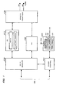
- FIG. 2 An example of the configuration of the sampling clock generation circuit (HSDLL circuit) in accordance with this embodiment is shown in Fig. 2.
- the HSPLL 22 multi-phase clock generation circuit outputs clocks CLK0, CLK1, CLK2, CLK3, and CLK4 (generally speaking: first to N-th clocks) of the same frequency but with mutually different phases. More specifically, it uses the outputs of five differential output comparators (generally speaking: first to N-th inversion circuits, in an odd number of stages) comprised by a VCO (an oscillation means with variably controlled oscillation frequency) to generate and output the clocks CLK0 to CLK4.
- a VCO an oscillation means with variably controlled oscillation frequency
- the HSDLL circuit 10 comprises an edge detection circuit 70 and a clock selection circuit 72.
- This edge detection circuit 70 detects an edge of data DIN that is input from the analog front-end circuit 430 and outputs that edge detection information to the clock selection circuit 72.
- the HSPLL 22 detects whether there is an edge of data DIN between any of either the rising or falling edges of CLK0 to CLK4 from the HSPLL 22, and outputs that edge detection information to the clock selection circuit 72.
- the clock selection circuit 72 selects one of the clocks CLK0 to CLK4 based on that edge detection information, then outputs the selected clock to the elasticity buffer 12 (see Fig. 1) in a later stage as a sampling clock SCLK.
- Timing waveform charts shown in Figs. 3A and 3B illustrate the operation of this embodiment of the present invention.
- the frequencies of CLK0 to CLK4 are clocks at the same 480 MHz. If the period of each clock is T, the phase between each pair of clocks is T/5 (generally speaking: T/N).
- Fig. 3A shows an example in which an edge ED of the data DIN that is being sampled is detected by the edge detection circuit 70 of Fig. 2 between the clocks CLK0 and CLK1. If that happens, the clock CLK3, which has an edge EC3 that is shifted by just three (generally speaking: a set number M) edges from the edge ED of the data DIN, is selected by the clock selection circuit 72 of Fig. 2, and the thus-selected CLK3 is output to the later-stage circuit (the elasticity buffer 12) as the DIN sampling clock SCLK.
- the clock CLK3 which has an edge EC3 that is shifted by just three (generally speaking: a set number M) edges from the edge ED of the data DIN
- the edge ED of DIN is detected by the edge detection circuit 70 between CLK2 and CLK3. If that happens, the clock CLK0 having an edge EC0 that is shifted by just three (generally speaking: the set number M) edges from the edge ED of DIN is selected by the clock selection circuit 72, by way of example, and the thus-selected CLK0 is output to the later-stage circuit (the elasticity buffer 12) as the DIN sampling clock SCLK.
- the sampling clock SCLK for the data DIN can be selected by a simple configuration in accordance with this embodiment by which the edge ED of the data DIN is detected and a clock is selected from CLK0 to CLK4, based on the thus-obtained edge detection information. It is therefore possible to generate a clock SCLK that is suitable for sampling DIN, even when DIN is fast transfer data that is synchronized with an external device at 480 MHz.
- This embodiment makes it possible to position the edge ES of the generated sampling clock SCLK close to the direct center of the edges of DIN, as shown in Figs. 3A and 3B. Since it is therefore possible to ensure sufficient set-up and hold times for holding data in the later-stage circuit (the elasticity buffer 12), it is possible to greatly increase the reliability of data reception.
- this embodiment utilizes the outputs of the differential output comparators (inversion circuits) within the VCO of the HSPLL 22 as the five-phase (multi-phase) clocks CLK0 to CLK4 used for detecting DIN edges and generating SCLK. It is therefore unnecessary to provide separate new circuitry for generating CLK0 to CLK4, making it possible to reduce the size of the circuitry.
- FIG. 4 A detailed example of the configuration of the HSPLL 22 is shown in Fig. 4.
- This HSPLL 22 comprises a phase comparator 80, a charge pump circuit 82, a filter circuit 84, a voltage-controlled oscillator (VCO) 86, and a clock divider 88.
- VCO voltage-controlled oscillator
- the phase comparator 80 compares the phases of a base clock RCLK (of, for example, 12 to 24 MHz) and a clock DCLK4 from the clock divider 88, then outputs a phase error signal PUP or PDW (where PUP is a phase-advanced signal and PDW is a phase-retarded signal).
- the charge pump circuit 82 operates a charge pump on the basis of the PUP or PDW signal from the phase comparator 80. More specifically, if PUP is active the charge pump circuit 82 charges a capacitor within the filter circuit 84; if PDW is active, it discharges the capacitor. A control voltage VC that has been smoothed by the filter circuit 84 is given to the VCO 86.
- the VCO 86 performs an oscillation operation wherein the oscillation frequency is controlled in a variable manner in accordance with the control voltage VC, to generate 480-MHz clocks QCLK0 to QCLK4. If the control voltage VC is high, by way of example, the oscillation frequency also increases; if the control voltage VC is low, the oscillation frequency also decreases.
- the clocks QCLK0, QCLK1, QCLK2, QCLK3, and QCLK4 generated by the VCO 86 are output to the exterior as CLK0, CLK2, CLK4, CLK1, and CLK3 through buffer circuits BF00 to BF04 and BF10 to BF14.
- buffer circuits BF00 to BF04 and BF10 to BF14 denote dummy buffer circuits for load-compensation with another buffer circuit BF24.
- the clock divider 88 divides (1/N) the clock QCLK4 that is input from the VCO 86 through the buffer circuits BF04 and BF24 and outputs the divided clock DCLK4 to the phase comparator 80.
- the HSPLL 22 configured as shown in Fig. 4 is capable of generating a high-frequency 480-MHz clock CLK4 (CLK0 to CLK3) that is phase-synchronized with the base clock RCLK.
- HSPLL 22 of Fig. 4 could also have a configuration such that the charge pump circuit 82 is not provided.
- a current-control oscillation means could be provided instead of the VCO 86.
- FIG. 5 An example of the configuration of the VCO 86 is shown in Fig. 5.
- This VCO 86 comprises five stages (generally speaking: an odd number of stages) of serially-connected differential output comparators DCP0 to DCP4 (generally speaking: inversion circuits), such that differential outputs XQ and Q of each of DCP0 to DCP4 are input to differential inputs I and XI of corresponding single-end output comparators SCP0 to SCP4 (generally speaking: buffer circuits) . Outputs of SCP0 to SCP4 become the output clocks QCLK0 to QCLK4 of the VCO 86.
- the output of the final-stage differential output comparator DCP4 is connected to the input of the initial-stage differential output comparator DCP0 by feedback lines FLA and FLB (feedback line pair). If the control voltage VC changes, the current flowing through the current source in the differential output comparators DCP0 to DCP4 also changes, so the oscillation frequency changes.
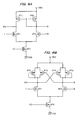
- Each of these differential output comparators comprises transistors NT1 and NT2, where the differential inputs I and XI are connected to the gate electrodes thereof and the differential outputs XQ and Q are connected to the drain electrodes thereof, and an n-type transistor NT3 (current source), where the control voltage VC is connected to the gate electrode thereof.
- the differential output comparator also comprises p-type transistors PT1 and PT2, where the differential output Q is connected to both gate electrodes thereof and the differential outputs XQ and Q are connected to the drain electrodes thereof.
- Each of these differential output comparators comprises n-type transistors NT4 and NT5, where the differential inputs I and XI are connected to the gate electrodes thereof and the differential outputs XQ and Q are connected to the drain electrodes thereof, an n-type transistor NT6 (current source), where the control voltage VC is connected to the gate electrode thereof.
- the differential output comparator also comprises p-type transistors PT3 and PT4, where the differential outputs Q and XQ are connected to the gate electrodes thereof and the differential outputs XQ and Q are connected to the drain electrodes thereof, and p-type transistors PT5 and PT6, where the differential outputs XQ and Q are connected to the gate and the drain electrodes thereof.
- the circuit of Fig. 6B forms a multi-vibrator type of comparator that has a configuration such that the components on the XQ side (PT3, PT5, and NT4) are line-symmetrical with the components on the Q side (PT4, PT6, and NT5).
- PT3 turns on and the potential of XQ rises
- PT4 turns on and the potential of Q rises. It is therefore possible to increase the amplitude of the differential outputs Q and XQ more than in the configuration of Fig. 6A (for example, to 1.4 V to 3.2 V).
- inversion circuits comprised within the VCO 86 are not limited to the differential output comparators shown in Figs. 6A and 6B, and thus various other modifications are possible.
- An inversion circuit shown by way of example in Fig. 7 has p-type transistors PT7 and PT8 and n-type transistors NT7 and NT8 connected in series. The current flowing through these transistors is controlled by control voltages VCQ and VC connected to the gate electrodes of PT7 and NT8, so that the oscillation frequency can be controlled in a variable manner.
- FIG. 8 An example of the configuration of the single-end output comparators SCP0 to SCP4 is shown in Fig. 8.
- the differential portion of the single-end output comparator shown in Fig. 8 comprises n-type transistors NT10 and NT11, where the differential inputs I and XI are connected to the gate electrodes thereof and nodes ND1 and ND2 are connected to the drain electrodes thereof, and an n-type transistor NT12 (current source), where a reference voltage VREF is connected to the gate electrode thereof.
- This differential portion also comprises p-type transistors PT10 and PT11, where the nodes ND2 and ND1 are connected to the gate electrodes thereof and the nodes ND1 and ND2 are connected to the drain electrodes thereof, and p-type transistors PT12 and PT13, where the nodes ND1 and ND2 are connected to the gate electrodes and the drain electrodes thereof.
- the output portion of the single-end output comparator of Fig. 8 comprises a p-type transistor PT14, where the node ND1 is connected to the gate electrode thereof and the drain electrode is connected to the single-end output Q, and an n-type transistor NT13 (current source), where the reference voltage VREF is connected to the gate electrode thereof and the drain electrode is connected to the single-end output Q.
- the outputs of the five-stage differential output comparators DCP0 to DCP4 (inversion circuits) of Fig. 5 are used to obtain the five-phase clock CLK0 to CLK4 described with reference to Figs. 2, 3A, and 3B.
- These differential output comparators DCP0 to DCP4 are essential for the oscillation operation of the VCO 86. Therefore, use of the outputs of those differential output comparators DCP0 to DCP4 in the generation of the five-phase clock CLK0 to CLK4 make it unnecessary to provide separate new circuits for generating CLK0 to CLK4, thus making the circuitry more compact.
- FIG. 9 An example of the configuration of the edge detection circuit 70 and the clock selection circuit 72 is shown in Fig. 9.
- the edge detection circuit 70 comprises a D flip-flop DFA0, D flip-flops DFB0 to DFB4 (first to N-th holding means), and detection circuits EDET0 to EDET4 (first to N-th detection means).
- the D flip-flop DFA0 samples and holds a signal SQUELCH based on edges of the data DIN and outputs a signal SSQUELCH.
- the D flip-flop DFB0 (the first holding means) samples and holds the data DIN by using the edge of the clock CLK0.
- DFB1 (the second holding means) holds DIN by using CLK1
- DFB2 (the third holding means) holds DIN by using CLK2
- DFB3 (the fourth holding means) holds DIN by using CLK3
- DFB4 (the fifth holding means) holds DIN by using CLK4.
- the detection circuits EDET0 to EDET4 perform exclusive-OR operations based on outputs DQ0 to DQ4 (held data) of the D flip-flops DFB0 to DFB4, to detect whether there is an edge of the data DIN between any of the edges of the clocks CLK0 to CLK4.
- the detection circuit EDET0 (the first detection means) detects whether or not there is an edge of the data DIN between edges of the clocks CLK0 and CLK1, based on the outputs DQ0 and DQ1 of the D flip-flops DFB0 and DFB1.
- EDET1 (the second detection means) detects whether or not there is an edge of DIN between edges of CLK1 and CLK2, based on the outputs DQ1 and DQ2 of DFB1 and DFB2.
- EDET2 detects whether or not there is an edge of DIN between edges of CLK2 and CLK3, based on the outputs DQ2 and DQ3 of DFB2 and DFB3
- EDET3 detects whether or not there is an edge of DIN between edges of CLK3 and CLK4, based on the outputs DQ3 and DQ4 of DFB3 and DFB4
- EDET4 detects whether or not there is an edge of DIN between edges of CLK4 and CLK0, based on the outputs DQ4 and DQ0 of DFB4 and DFB0.
- the clock selection circuit 72 selects one of the clocks CLK0 to CLK4 on the basis of the outputs EQ0 to EQ4 (edge detection information) of the detection circuits EDET0 to EDET4, and outputs the selected clock as the sampling clock SCLK.
- Timing waveform charts shown in Figs. 10 and 11 illustrate the operation of this embodiment.
- the D flip-flops DFB0 to DFB4 hold the data DIN at the rising edges of CLK0 to CLK4 and output DQ0 to DQ4, as shown at B1 in Fig. 11.
- the detection circuit EDET0 performs an exclusive-OR operation on DQ0 and DQ1, by way of example, and outputs EQ0, as shown at B2.
- the detection circuits EDET1, EDET2, EDET3, and EDET4 perform exclusive-OR operations on DQ1 and DQ2, DQ2 and DQ3, DQ3 and DQ4, and DQ4 and DQ0, to output EQ1 to EQ4.
- the clock selection circuit 72 determines which of the clocks CLK0 to CLK4 is to be selected based on these outputs EQ0 to EQ4. Since an edge of the data is detected between the edges of the clocks CLK0 and CLK1 in the example shown at B2 in Fig. 11, the clock CLK4 that has three edges (given set number M) from the edge of DIN is selected (see Fig. 3A) and output as the sampling clock SCLK.
- This clock selection can be implemented by a combinational circuit (not shown in the figure) within clock selection circuit 72 that generates clock selection signals CSEL0 to CSEL4 as shown in Fig. 10, then performing logical operations on these CSEL0 to CSEL4 signals and CLK0 to CLK4.
- the clock selection signal CSEL3 goes active (to 1) at A3 in Fig. 10 in this example, the clock CLK3 is selected and output as the sampling clock SCLK.
- CSEL2 and CSEL1 go active at A4 and A5, CLK2 and CLK1 are selected in each case, for output as SCLK.
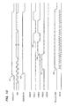
- edge ED of the data DIN and an edge EC1 of CLK1 come close at C1 in Fig. 12, so the set-up time TS for the D flip-flop DFB1 (see Fig. 9) which holds DIN at CLK1 is insufficient.
- the held data becomes "undefined" at C2 in Fig. 12, so it is not possible to determine whether it is 0 or 1.
- this embodiment ensures that the clock that holds an edge that is shifted by just three (M) edges from the edge ED of DIN (the position at wich ED is assumed to be detected) is selected as the sampling clock SCLK, as shown at C3 and C4 in Fig. 12, so a suitable SCLK can be generated.
- the fetched edge of SCLK can be positioned close to the center between the rising edge and the falling edge of DIN, as shown at C4 in Fig. 12, even if CLK3 is selected as SCLK as shown at C3 or if CLK4 is selected as SCLK as shown at C4. It is therefore possible for the later-stage circuit (elasticity buffer) to use the thus-generated SCLK to sample and hold DIN.
- Equation (1) N ⁇ T/(TS + TH) or: N ⁇ [T/(TS + TH)] where [X] in Equation (3) is the maximum integer that does not exceed X.
- the hold time TH for the D flip-flop DFB0 (see Fig. 9) that holds DIN at CLK0 is not sufficient.
- the held data therefore becomes undefined, as shown at D2, so that it is no longer possible to verify whether it is 0 or 1.
- edge ED of DIN and the edge EC1 of CLK1 are close at D3 in Fig. 13A, so the set-up time TS for the D flip-flop DFB1 that holds DIN at CLK1 is not sufficient. This means that the held data becomes undefined, as shown at D4, so that it is no longer possible to verify whether it is 0 or 1.
- the number N of multi-phase clocks is preferably set in such a manner as to satisfy the relationship N ⁇ [T/(TS + TH)].
- CLK2 is selected at E1 in Fig. 13B and CLK0 is selected at E2.
- the configuration shown in Fig. 12 has the advantage of making it possible to select a clock having an edge that is shifted between two and four edges from the edge ED of DIN, thus broadening the selection range for selectable clocks.
- N 5
- N 5
- the number of inversion circuit stages of the HSPLL 22 can be set to five and high-frequency oscillation of the VCO (oscillation circuit) of the HSPLL 22 can be ensured. As a result, it is possible to obtain a high-frequency sampling clock.
- sampling clock SCLK generated by the sampling clock generation circuit of this embodiment is used directly in the sampling of the data DIN, it is preferable that a clock that is positioned close to the direct center between rising and falling edges of DIN is used as SCLK, as shown in Fig. 14A.
- the clock CLK3 that has an edge that is shifted just three (the set number M) edges from the edge ED of the data DIN is selected as the sampling clock SCLK.
- the later-stage circuitry does not use the sampling clock SCLK from the sampling clock generation circuit directly but instead uses a clock SCLK' which is obtained by applying a logical operation to SCLK.
- the clock CLK2 having an edge that is shifted by just two edges from the edge ED of the data DIN is selected as SCLK, as shown by way of example in Fig. 14B.
- the later-stage circuit uses SCLK', which is a clock obtained by subjecting this SCLK to a logical operation or the like, for holding the data DIN. This makes it possible to ensure sufficient set-up and hold times when the later-stage circuit holds DIN.
- the number of edge M of the shift from the edge ED of DIN is preferably set to be variable in accordance with the configuration of the later-stage circuit.
- DIN could also be delayed by a delay element before output to the later-stage circuit, so that the data DIN can be sampled in a suitable manner by SCLK'.
- Fig. 15 An example of the configuration of the elasticity buffer 12 that is a later-stage circuit is shown in Fig. 15. Note that the elasticity buffer 12 is a circuit comprised within the HS circuit 410, and a determination circuit 60, a buffer 64, and a selector 66 are comprised within another component such as the data handler circuit 400 of Fig. 1, by way of example.
- the elasticity buffer 12 comprises a data holding register 50 (data holding means), a data status register 52 (data status holding means), and a write pulse generation circuit 54 (write pulse generation means).
- the data holding register 50 is a 32-bit wide register that receives the serial data DIN and holds it.
- the data status register 52 is a 32-bit wide register that holds the status of each bit of data in the data holding register 50.
- the write pulse generation circuit 54 generates a 32-bit wide write pulse signal WP [0: 31] and outputs it to the data holding register 50 and the data status register 52.
- the write pulse signal WP [0: 31] is a signal in which each pulse goes active periodically every 32 clock cycles of the sampling clock SCLK (generally speaking: every K-th clock cycle) and the periods at which each pulse goes active are each shifted by one clock cycle.
- the data holding register 50 holds each bit of data, based on the write pulse signal WP [0: 31].
- the data status register 52 holds the status of each bit of data, based on the write pulse signal WP[0: 31].
- the determination circuit 60 (determination means) is a circuit which determines whether or not data that is held in the data holding register 50 is valid, in data cell units configured of a plurality of bits (such as 8 bits), and which operates in accordance with an internal status machine 62.
- the determination circuit 60 receives from the data status register 52 a 4-bit wide signal VALID[0: 3] that indicates whether or not each data cell of the data holding register 50 is valid and a signal OVFLOW that becomes active when the data holding register 50 overflows.
- each data cell determines whether or not each data cell is valid and outputs to the selector 66 a signal SEL for selecting valid data cells. It also outputs to the data status register 52 a signal STRB[0: 3] for clearing the data statuses held in the data status register 52, in data cell units. Furthermore, it outputs to the elasticity buffer 12 a signal TERM that goes active at the completion of packet reception in HS mode and a signal HSENB that enables reception in HS mode.
- the buffer 64 receives 32-bit wide parallel data DPA[0: 31] from the data holding register 50 and outputs data DBUF[0: 31], which has been synchronized by a 60-MHz clock PCLK and buffered, to the selector 66.
- the selector 66 (output means) selects data in valid data cells from the data DBUF[0: 31] from the buffer 64, based on the signal SEL from the determination circuit 60, and outputs it as 8-bit wide data DOUT[0: 7].
- the elasticity buffer 12 of Fig. 15 uses the write pulse signal WP[0: 31] from the write pulse generation circuit 54 for the holding of data by the data holding register 50, not SCLK from the sampling clock generation circuit.
- WP [0: 31] which is generated by subjecting SCLK to a logical operation or the like. It is therefore desirable to determine the set number M from consideration of element delay due to the write pulse generation circuit 54 when selecting the clock, as described with reference to Figs. 14A and 14B.
- FIG. 16 An example of the layout of the inversion circuits DCP0 to DCP4 (differential output comparators) and buffer circuits SCP0 to SCP4 (single-end output comparators) of Fig. 5 and the buffer circuits BF00 to BF04, BF20 to BF24, and BF10 to BF14 of Fig. 4 is shown in Fig. 16.
- the inversion circuits DCP0 to DCP4 are disposed along a line LN1 (first line) that is parallel to a feedback line FL (the feedback line pair FLA and FLB of Fig. 5), whereas the buffer circuits SCP0 to SCP4 are disposed along a line LN2 (second line) that is also parallel to FL but differs from LN1.
- LN1 first line
- LN2 second line
- This configuration makes it possible to shorten the length of the feedback line FL and reduce the parasitic capacitance of the feedback line FL, in comparison to a method by which the inversion circuits DCP0 to DCP4 and the buffer circuits SCP0 to SCP4 are all disposed along the same line. It is therefore possible to obtain a high-frequency clock and also ensure that the phase differences between the multi-phase clocks (differences in signal delays) are equal (equivalent).
- Fig. 16 also shows that the feedback line FL is disposed in a region between the inversion circuits DCP0 to DCP4 and the buffer circuits SCP0 to SCP4. This makes it possible to substitute a line connecting the inversion circuit DCP4 and the buffer circuit SCP4 for the feedback line and prevent the addition of excess parasitic capacitance to the output of the inversion circuit DCP4.
- a dummy line DL (DLA0 to DLA3 and DLB0 to DLB3) is provided, and the dummy line DL and the feedback line FL are disposed in the region between the inversion circuits DCP0 to DCP4 and the buffer circuits SCP0 to SCP4. This ensures that the parasitic capacitances of the outputs of the inversion circuits DCP0 to DCP4 can be made equal, making it possible to generate multi-phase clocks having substantially the same phase difference (signal delay difference), but shifted sequentially.
- the outputs of the inversion circuits DCP0 to DCP3 are provided with dummy lines DLA0 to DLA3 and DLB0 to DLB3 (equivalent to DL in Fig. 16), which have parasitic capacitances that are equal (including cases in which they are substantially equal) to the parasitic capacitances of the feedback lines FLA and FLB (equivalent to FL in Fig. 16) connected to the output of the final-stage inversion circuit DCP4.
- dummy lines DLA0 to DLA3 and DLB0 to DLB3 are disposed parallel to the feedback lines FLA and FLB.
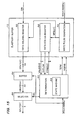
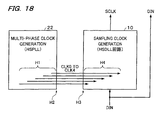
- the sampling clock generation circuit uses the multi-phase clocks CLK0 to CLK4 (first to N-th clocks) generated by the multi-phase clock generation circuit (the HSPLL 22 of Fig. 2) to generate the sampling clock SCLK for sampling the data DIN, as shown in Fig. 18.
- the interconnection of the lines CLK0 to CLK4 in accordance with this embodiment is done in such a manner that the parasitic capacitances of the lines of the clocks CLK0 to CLK4 (the lines connected to the outputs of the buffer circuits BF10 to BF14 of Fig. 16) are equal (including cases in which they are substantially equal).
- the interconnection of the lines for CLK0 to CLK4 on the multi-phase clock generation circuit 22 side of Fig. 18 could be done as shown in Fig. 19 by way of example.
- these lines are made to be deliberately curved, in such a manner that the lengths of the lines of the clocks CLK0 to CLK4 on the multi-phase clock generation circuit 22 side are equal (or substantially equal), as shown in Fig. 19.
- This configuration makes it possible to ensure that the parasitic capacitances of the lines for CLK0 to CLK4 are equal within the portion up to the output terminals of the multi-phase clock generation circuit 22 (denoted by H2 in Fig. 18).
- the interconnection of CLK0 to CLK4 in the portion from the output terminals of the multi-phase clock generation circuit 22 (denoted by H2) to the input terminals of the sampling clock generation circuit 10 (denoted by H3) is done in such a manner that the parasitic capacitances of the lines for CLK0 to CLK4 are equal.
- the lengths of the lines for CLK0 to CLK4 are equal in the portion between H2 and H3.
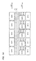
- Fig. 20 shows that the layout ensures that the lengths of the lines for CLK0 to CLK4 are equal from the input terminals of the sampling clock generation circuit 10 (denoted by H3) to the D terminals DT0 to DT4 of the D flip-flops DFB0 to DFB4 (see Fig. 9).
- the D flip-flops DFB0 to DFB4 (first to N-th holding circuits) that hold the data DIN by using the clocks CLK0 to CLK4 are disposed along a line LN3 that is parallel to the lines for CLK0 to CLK4, as shown in Fig. 20.
- the lines for the clocks CLK0 to CLK4 are connected to the corresponding D terminals DT0 to DT4 (DFB0 to DFB4 inputs) of the D flip-flops DFB0 to DFB4 after looping back at loop-back points TPT0 to TPT4 (first to N-th loop-back points).
- these loop-back points TPT0 to TPT4 are provided at locations where the parasitic capacitances of the lines for CLK0 to CLK4 are mutually equal.
- This configuration makes it possible to ensure that the parasitic capacitances of the lines for CLK0 to CLK4 on the sampling clock generation circuit 10 side are mutually equal.
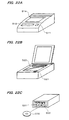
- FIG. 21A An internal block diagram of a printer that is one example of such electronic equipment is shown in Fig. 21A with an external view thereof being shown in Fig. 22A.
- a CPU (microcomputer) 510 has various functions, including that of controlling the entire system.
- An operating section 511 is designed to enable the user to operate the printer.
- Data such as a control program and fonts is stored in a ROM 516, and a RAM 517 functions as a work area for the CPU 510.
- a DMAC 518 is a DMA controller for transferring data through the CPU 510.
- a display panel 519 is designed to inform the user of the operational state of the printer.
- Serial print data that has been send in from another device such as a personal computer via USB is converted into parallel print data by a data transfer control device 500.
- the thus converted parallel print data is sent to a print processing section (a printer engine) 512 by the CPU 510 or the DMAC 518.
- This parallel print data is subjected to given processing in the print processing section 512 and is output for printing to paper by a printing section (a device for outputting data) 514 comprising components such as a print head.
- FIG. 21B An internal block diagram of a scanner that is another example of electronic equipment is shown in Fig. 21B with an external view thereof being shown in Fig. 22B.
- a CPU 520 has various functions, including that of controlling the entire system.
- An operating section 521 is designed to enable the user to operate the scanner.
- Data such as a control program is stored in a ROM 526, and a RAM 527 functions as a work area for the CPU 520.
- a DMAC 528 is a DMA controller.
- An image of a document is read in by an image read section (a device for fetching data) 522, which comprises components such as a light source and an opto-electric converter, and data of the read-in image is processed by an image processing section (a scanner engine) 524.
- the processed image data is sent directly to the data transfer control device 500 by the CPU 520 or DMAC 528.
- the data transfer control device 500 converts that parallel image data into serial data and sends it to another device such as a personal computer via USB.
- FIG. 21C An internal block diagram of a CD-RW drive that is a further example of electronic equipment is shown in Fig. 21C with an external view thereof being shown in Fig. 22C.
- a CPU 530 has various functions, including that of controlling the entire system.
- An operating section 531 is designed to enable the user to operate the CD-RW drive.
- Data such as a control program is stored in a ROM 536, and a RAM 537 functions as a work area for the CPU 530.
- a DMAC 538 is a DMA controller.
- the data that has been subjected to this signal processing is sent to the data transfer control device 500 by the CPU 530 or the DMAC 538.
- the data transfer control device 500 converts this parallel data into serial data, then sends it to another device such as a personal computer via USB.
- Serial data that comes in from another device via USB is converted into parallel data by the data transfer control device 500.
- This parallel data is sent to the signal processing section 534 by the CPU 530 or the DMAC 538.
- This parallel data is subjected to given signal processing by the signal processing section 534 then is stored by the read/write section 533 on the CD-RW 532.
- a separate CPU for data transfer control by the data transfer control device 500 could be provided in addition to the CPU 510, 520, or 530 of Fig. 21A, 21B, or 21C.
- Use of the data transfer control device of this embodiment in electronic equipment also enables the fabrication of an IC for the data transfer control device by ordinary semiconductor processes, which have low fabrication costs. It is therefore possible to reduce the price of the data transfer control device and thus reduce the price of the electronic equipment. Since the number of components that operate at high speed during data transfer control can be reduced, it is possible to increase the reliability of data transfer, thus increasing the reliability of the electronic equipment.
- the electronic equipment that can employ a data transfer control device in accordance with the present invention is not limited to the above described embodiments, and thus various other examples can be considered, such as various types of optical disk drive (CD-ROM or DVD), magneto-optical (MO) disk drives, hard disk drives, TVs, VCRs, video cameras, audio equipment, telephones, projectors, personal computers, electronic organizers, and dedicated wordprocessors.
- CD-ROM or DVD compact disc-ROM or DVD
- MO magneto-optical
- the configuration of the data transfer control device in accordance with the present invention is not limited to that shown in Fig. 1.
- edge detection means edge detection circuit
- clock selection means clock selection circuit
- the number of multi-phase clocks N is not limited to five.
- the sampling clock generation circuit it may be possible to shorten the set-up time TS and the hold time TH further, by way of example. In such a case, therefore, it would be possible to increase the number of clocks to more than five.
- the present invention can also be applied to data transfer in accordance with a standard that is based on a concept similar to that of USB 2.0, or a standard that is developed from USB 2.0.
Landscapes
- Engineering & Computer Science (AREA)
- Theoretical Computer Science (AREA)
- Physics & Mathematics (AREA)
- General Engineering & Computer Science (AREA)
- General Physics & Mathematics (AREA)
- Computer Networks & Wireless Communication (AREA)
- Signal Processing (AREA)
- Synchronisation In Digital Transmission Systems (AREA)
- Information Transfer Systems (AREA)
- Stabilization Of Oscillater, Synchronisation, Frequency Synthesizers (AREA)
- Communication Control (AREA)
Abstract
Description
wherein, when a set-up time of the holding circuit comprised by the edge detection circuit is TS, a hold time of the holding circuit comprised by the edge detection circuit is TH, and a period of each of the first to N-th clocks is T, number of clocks N of the first to N-th clocks is such that: N ≦ [T/(TS + TH)] (where [X] is a maximum integer that does not exceed X).
Claims (18)
- A sampling clock generation circuit which generates a sampling clock used for sampling data, the sampling clock generation circuit comprising:an edge detection circuit detecting between which two edges a data edge is located, the two edges being among edges of first to N-th clocks having the same frequency but mutually different phases; anda clock selection circuit which selects one clock from among the first to N-th clocks, based on detection information from the edge detection circuit, and outputs the selected clock as the sampling clock.
- The sampling clock generation circuit as defined by claim 1,
wherein the edge detection circuit comprises:wherein the clock selection circuit selects a clock from among the first to N-th clocks, based on edge detection information from the first to N-th detection circuits, and outputs the selected clock as the sampling clock.a first holding circuit which holds data by using the first clock,... a J-th holding circuit which holds data by using a J-th clock (where: 1 < J < N), ... and an N-th holding circuit which holds data by using the N-th clock; anda first detection circuit which detects whether or not there is a data edge between the edges of the first clock and a second clock, based on data held in the first holding circuit and a second holding circuit, ... a J-th detection circuit which detects whether or not there is a data edge between the edges of the J-th clock and a (J + 1)-th clock, based on data held in the J-th holding circuit and a (J + 1)-th holding circuit, ... and an N-th detection circuit which detects whether or not there is a data edge between the edges of the N-th clock and the first clock, based on data held in the N-th and first holding circuits, and - The sampling clock generation circuit as defined by claim 2,
wherein, when a set-up time of the first to N-th holding circuits is TS, a hold time of the first to N-th holding circuits is TH, and a period of each of the first to N-th clocks is T, number of clocks N of the first to N-th clocks is such that: N ≤ [T/(TS + TH)] (where [X] is a maximum integer that does not exceed X). - The sampling clock generation circuit as defined by claim 3,
wherein number of clocks N is such that N = [T/(TS + TH)] (where [X] is a maximum integer that does not exceed X). - The sampling clock generation circuit as defined by any one of claims 1 to 4,
wherein the number of clocks N of the first to N-th clocks is such that N = 5. - The sampling clock generation circuit as defined by any one of claims 1 to 5,
wherein the clock selection circuit selects from the first to N-th clocks a clock having an edge that is shifted by a given set number M of edges from a data edge, and outputs the selected clock as the sampling clock. - The sampling clock generation circuit as defined by claim 6,
wherein the number M is set to a number that ensures a set-up time and a hold time of a circuit which holds data based on the generated sampling clock. - A sampling clock generation circuit which generates a sampling clock used for sampling data, the sampling clock generation circuit comprising:wherein the edge detection circuit comprises at least one holding circuit which holds data at any clock from among the first to N-th clocks, andan edge detection circuit which detects a data edge; anda clock selection circuit which selects a clock from among first to N-th clocks having the same frequency but mutually different phases, based on detection information from the edge detection circuit, and outputs the selected clock as the sampling clock,
wherein, when a set-up time of the holding circuit comprised by the edge detection circuit is TS, a hold time of the holding circuit comprised by the edge detection circuit is TH, and a period of each of the first to N-th clocks is T, number of clocks N of the first to N-th clocks is such that: N ≦ [T/(TS + TH)] (where [X] is a maximum integer that does not exceed X). - The sampling clock generation circuit as defined by claim 8,
wherein number of clocks N is such that N = [T/(TS + TH)] (where [X] is a maximum integer that does not exceed X). - The sampling clock generation circuit as defined by claim 8 or 9,
wherein the number of clocks N of the first to N-th clocks is such that N = 5. - A sampling clock generation circuit which generates a sampling clock used for sampling data, the sampling clock generation circuit comprising:wherein the clock selection circuit selects from the first to N-th clocks a clock having an edge that is shifted by a given set number M of edges from the data edge, and outputs the selected clock as the sampling clock.an edge detection circuit which detects a data edge; anda clock selection circuit which selects a clock from among first to N-th clocks having the same frequency but mutually different phases, based on detection information from the edge detection circuit, and outputs the selected clock as the sampling clock,
- The sampling clock generation circuit as defined by claim 11,
wherein the number M is set to a number that ensures a set-up time and a hold time of a circuit which holds data based on the generated sampling clock. - The sampling clock generation circuit as defined by any one of claims 1 to 12, further comprising:wherein the first to N-th clocks is generated based on outputs of first to N-th inversion circuits of an odd number of stages included in the oscillation circuit.a PLL circuit having an oscillation circuit with a variably-controlled oscillation frequency, and phase-synchronizing a clock generated by the oscillation circuit with a base clock,
- The sampling clock generation circuit as defined by claim 13,
wherein at least one of a disposition of the first to N-th inversion circuits and interconnection of output lines of the first to N-th inversion circuits is performed in such a manner that phase differences between the first to N-th clocks are equal. - The sampling clock generation circuit as defined by claim 13 or 14,
wherein lines for the first to N-th clocks are interconnected in such a manner that the parasitic capacitances of lines of the first to N-th clocks are equal. - A data transfer control device for providing data transfer over a bus, the data transfer control device comprising:the sampling clock generation circuit as defined by any one of claims 1 to 15; anda circuit which holds data, based on the sampling clock generated by the sampling clock generation circuit, and performs given processing for data transfer, based on the held data.
- The data transfer control device as defined by claim 16,
wherein data transfer is in accordance with the Universal Serial Bus (USB) standard. - Electronic equipment comprising:the data transfer control device as defined by claim 16 or 17; anda device which performs output processing, fetch processing or storage processing on data transferred through the data transfer control device and the bus.
Applications Claiming Priority (4)
| Application Number | Priority Date | Filing Date | Title |
|---|---|---|---|
| JP2000319722 | 2000-10-19 | ||
| JP2000319722 | 2000-10-19 | ||
| JP2001098350A JP3622685B2 (en) | 2000-10-19 | 2001-03-30 | Sampling clock generation circuit, data transfer control device, and electronic device |
| JP2001098350 | 2001-03-30 |
Publications (3)
| Publication Number | Publication Date |
|---|---|
| EP1199837A2 true EP1199837A2 (en) | 2002-04-24 |
| EP1199837A3 EP1199837A3 (en) | 2003-07-02 |
| EP1199837B1 EP1199837B1 (en) | 2006-12-20 |
Family
ID=26602428
Family Applications (1)
| Application Number | Title | Priority Date | Filing Date |
|---|---|---|---|
| EP01124703A Expired - Lifetime EP1199837B1 (en) | 2000-10-19 | 2001-10-16 | Sampling clock generation circuit, data transfer control device, and electronic equipment |
Country Status (8)
| Country | Link |
|---|---|
| US (1) | US20020047738A1 (en) |
| EP (1) | EP1199837B1 (en) |
| JP (1) | JP3622685B2 (en) |
| KR (1) | KR100397590B1 (en) |
| CN (1) | CN1165850C (en) |
| AT (1) | ATE349115T1 (en) |
| DE (1) | DE60125307D1 (en) |
| TW (1) | TWI243297B (en) |
Cited By (5)
| Publication number | Priority date | Publication date | Assignee | Title |
|---|---|---|---|---|
| WO2003036853A1 (en) * | 2001-10-26 | 2003-05-01 | International Business Machines Corporation | Transition detection, validation and memorization circuit |
| RU2244385C1 (en) * | 2003-08-27 | 2005-01-10 | Федеральное Государственное унитарное предприятие Воронежский научно-исследовательский институт связи | Signal phase selector |
| EP1545046A3 (en) * | 2003-12-19 | 2006-11-22 | IBM Corporation | Improvements to data recovery circuits using oversampling for best data sample selection |
| EP1545047A3 (en) * | 2003-12-19 | 2006-11-22 | International Business Machines Corporation | Improvements to data recovery circuits using oversampling for ISI compensation |
| GB2438286A (en) * | 2006-04-26 | 2007-11-21 | Realtek Semiconductor Corp | Output clock synchronisation using first and second delayed versions of an input clock |
Families Citing this family (29)
| Publication number | Priority date | Publication date | Assignee | Title |
|---|---|---|---|---|
| JP4031671B2 (en) * | 2002-06-11 | 2008-01-09 | 松下電器産業株式会社 | Clock recovery circuit |
| CN100420153C (en) * | 2002-08-23 | 2008-09-17 | 联发科技股份有限公司 | PLL |
| TW589831B (en) | 2002-12-05 | 2004-06-01 | Via Tech Inc | Multi-port network interface circuit and related method for triggering transmission signals of multiple ports with clocks of different phases |
| CN100352194C (en) * | 2003-04-23 | 2007-11-28 | 华为技术有限公司 | Method and device for guaranteeing reliable receiving syncronous data by tuning sampling clock |
| US7567629B2 (en) * | 2003-04-29 | 2009-07-28 | Jesper Jonas Fredriksson | Multiphase clock recovery |
| JP2005328138A (en) * | 2004-05-12 | 2005-11-24 | Ricoh Co Ltd | Phase adjuster |
| KR100674921B1 (en) * | 2004-11-24 | 2007-01-26 | 삼성전자주식회사 | Digital Data Sampling Blocks and Sampling Methods |
| CN100512009C (en) * | 2004-12-29 | 2009-07-08 | 旺玖科技股份有限公司 | System and method for oversampling high speed clock/data recovery |
| KR100936201B1 (en) * | 2005-03-31 | 2010-01-11 | 후지쯔 가부시끼가이샤 | Clock selecting circuit and synthesizer |
| WO2007060756A1 (en) * | 2005-11-22 | 2007-05-31 | Matsushita Electric Industrial Co., Ltd. | Phase comparator and regulation circuit |
| JP2007172574A (en) * | 2005-11-25 | 2007-07-05 | Seiko Epson Corp | Integrated circuit device and electronic apparatus |
| JP2007312321A (en) * | 2006-05-22 | 2007-11-29 | Sharp Corp | Semiconductor integrated circuit for serial / parallel conversion |
| KR100866603B1 (en) * | 2007-01-03 | 2008-11-03 | 삼성전자주식회사 | Data processing method and data processing device for deserializing and serializing |
| WO2008138053A1 (en) * | 2007-05-15 | 2008-11-20 | Fiberbyte Pty Ltd | Usb based synchronization and timing system |
| WO2009047706A1 (en) * | 2007-10-12 | 2009-04-16 | Nxp B.V. | Clock optimization and clock tree design method |
| US8139697B2 (en) | 2008-01-29 | 2012-03-20 | United Microelectronics Corp. | Sampling method and data recovery circuit using the same |
| CN101521567B (en) * | 2008-02-25 | 2011-06-15 | 联华电子股份有限公司 | Sampling method and its data recovery circuit |
| TWI362834B (en) | 2008-05-26 | 2012-04-21 | Novatek Microelectronics Corp | Differential transmitter and auto-adjustment method of data strobe thereof |
| JP5369524B2 (en) * | 2008-07-23 | 2013-12-18 | 株式会社リコー | Clock data recovery circuit |
| KR100980405B1 (en) * | 2008-10-13 | 2010-09-07 | 주식회사 하이닉스반도체 | DLD circuit |
| CN102347813B (en) * | 2011-09-26 | 2015-11-25 | 华为技术有限公司 | A kind of method and apparatus of selecting sampling clock signal |
| US9083478B2 (en) * | 2012-09-21 | 2015-07-14 | Altera Corporation | Apparatus and methods for determining latency of a network port |
| US9787468B2 (en) * | 2014-04-22 | 2017-10-10 | Capital Microelectronics Co., Ltd. | LVDS data recovery method and circuit |
| JP6737642B2 (en) * | 2016-06-14 | 2020-08-12 | ローム株式会社 | Serial data receiving circuit, receiving method, transceiver circuit, electronic device |
| CN106771990B (en) * | 2016-12-07 | 2020-01-24 | 武汉新芯集成电路制造有限公司 | Measuring circuit and measuring method for D trigger setup time |
| US10649486B1 (en) | 2016-12-28 | 2020-05-12 | Intel Corporation | Apparatus and methods for accurate latency measurements in integrated circuits |
| CN108345554B (en) * | 2017-01-22 | 2020-08-21 | 联发科技股份有限公司 | Method for determining sampling phase of sampling clock signal and related electronic device |
| CN109213703B (en) * | 2017-06-30 | 2021-12-14 | 华为技术有限公司 | Data detection method and data detection device |
| CN115878536A (en) * | 2022-11-11 | 2023-03-31 | 珠海天威技术开发有限公司 | Communication method of serial bus, data signal sampling circuit and sampling method of serial bus |
Family Cites Families (12)
| Publication number | Priority date | Publication date | Assignee | Title |
|---|---|---|---|---|
| US4672639A (en) * | 1984-05-24 | 1987-06-09 | Kabushiki Kaisha Toshiba | Sampling clock pulse generator |
| US4975702A (en) * | 1990-03-15 | 1990-12-04 | Intel Corporation | CMOS waveform digitizer |
| JPH0773598A (en) * | 1993-06-29 | 1995-03-17 | Hitachi Ltd | Timing extraction circuit and recording / reproducing apparatus using the same |
| JP3329088B2 (en) * | 1994-02-16 | 2002-09-30 | 株式会社デンソー | Pulse generator, variable frequency oscillator and PLL device |
| EP0809886A1 (en) * | 1995-02-16 | 1997-12-03 | Telefonaktiebolaget Lm Ericsson | A fast sigma-delta modulator having a controlled clock generator |
| JP2773669B2 (en) * | 1995-03-01 | 1998-07-09 | 日本電気株式会社 | Digital PLL circuit |
| US6081305A (en) * | 1995-05-30 | 2000-06-27 | Hitachi, Ltd. | Liquid crystal light valve and projection type liquid crystal display using such valve |
| EP0895378B1 (en) * | 1996-05-07 | 2006-03-08 | Yamaha Corporation | Method and system for transmitting audio data with time stamp |
| JP2877205B2 (en) * | 1996-08-28 | 1999-03-31 | 日本電気株式会社 | Two-phase non-overlap signal generation circuit |
| US5742188A (en) * | 1996-12-10 | 1998-04-21 | Samsung Electronics., Ltd. | Universal input data sampling circuit and method thereof |
| JP3109465B2 (en) * | 1997-12-04 | 2000-11-13 | 日本電気株式会社 | Digital PLL circuit and signal reproducing method |
| JP2000031951A (en) * | 1998-07-15 | 2000-01-28 | Fujitsu Ltd | Burst synchronization circuit |
-
2001
- 2001-03-30 JP JP2001098350A patent/JP3622685B2/en not_active Expired - Fee Related
- 2001-10-16 US US09/977,338 patent/US20020047738A1/en not_active Abandoned
- 2001-10-16 DE DE60125307T patent/DE60125307D1/en not_active Expired - Lifetime
- 2001-10-16 AT AT01124703T patent/ATE349115T1/en not_active IP Right Cessation
- 2001-10-16 EP EP01124703A patent/EP1199837B1/en not_active Expired - Lifetime
- 2001-10-18 TW TW090125833A patent/TWI243297B/en not_active IP Right Cessation
- 2001-10-18 KR KR10-2001-0064264A patent/KR100397590B1/en not_active Expired - Fee Related
- 2001-10-19 CN CNB011385138A patent/CN1165850C/en not_active Expired - Fee Related
Cited By (7)
| Publication number | Priority date | Publication date | Assignee | Title |
|---|---|---|---|---|
| WO2003036853A1 (en) * | 2001-10-26 | 2003-05-01 | International Business Machines Corporation | Transition detection, validation and memorization circuit |
| RU2244385C1 (en) * | 2003-08-27 | 2005-01-10 | Федеральное Государственное унитарное предприятие Воронежский научно-исследовательский институт связи | Signal phase selector |
| EP1545046A3 (en) * | 2003-12-19 | 2006-11-22 | IBM Corporation | Improvements to data recovery circuits using oversampling for best data sample selection |
| EP1545047A3 (en) * | 2003-12-19 | 2006-11-22 | International Business Machines Corporation | Improvements to data recovery circuits using oversampling for ISI compensation |
| GB2438286A (en) * | 2006-04-26 | 2007-11-21 | Realtek Semiconductor Corp | Output clock synchronisation using first and second delayed versions of an input clock |
| GB2438286B (en) * | 2006-04-26 | 2008-06-25 | Realtek Semiconductor Corp | Phase selector for data transmitting device |
| US7936857B2 (en) | 2006-04-26 | 2011-05-03 | Realtek Semiconductor Corp. | Phase selector for data transmitting device |
Also Published As
| Publication number | Publication date |
|---|---|
| JP3622685B2 (en) | 2005-02-23 |
| KR100397590B1 (en) | 2003-09-13 |
| US20020047738A1 (en) | 2002-04-25 |
| KR20020033433A (en) | 2002-05-06 |
| DE60125307D1 (en) | 2007-02-01 |
| CN1350234A (en) | 2002-05-22 |
| ATE349115T1 (en) | 2007-01-15 |
| CN1165850C (en) | 2004-09-08 |
| EP1199837B1 (en) | 2006-12-20 |
| TWI243297B (en) | 2005-11-11 |
| JP2002198941A (en) | 2002-07-12 |
| EP1199837A3 (en) | 2003-07-02 |
Similar Documents
| Publication | Publication Date | Title |
|---|---|---|
| EP1199837B1 (en) | Sampling clock generation circuit, data transfer control device, and electronic equipment | |
| US6990597B2 (en) | Clock generation circuit, data transfer control device, and electronic instrument | |
| US5987081A (en) | Method and apparatus for a testable high frequency synchronizer | |
| USRE40990E1 (en) | Data transmission across asynchronous time domains using phase-shifted data packet | |
| JP3587162B2 (en) | Data transfer control device and electronic equipment | |
| US20030160644A1 (en) | High-speed fully balanced differential flip-flop with reset | |
| EP0977109A1 (en) | Method and apparatus for synchronizing data transfers in a logic circuit having plural clock domains | |
| US6172540B1 (en) | Apparatus for fast logic transfer of data across asynchronous clock domains | |
| US11550749B2 (en) | Serial data interface with reduced loop delay | |
| US7242737B2 (en) | System and method for data phase realignment | |
| US6205191B1 (en) | Method and apparatus for synchronizing a control signal | |
| US6397374B1 (en) | Zero hold time circuit for high speed bus applications | |
| US6407682B1 (en) | High speed serial-deserializer receiver | |
| JP2005312053A (en) | Cross-coupled voltage controlled oscillator | |
| US7844843B2 (en) | Implementing power savings in HSS clock-gating circuit | |
| JP3415891B2 (en) | Packet data playback system | |
| CN120200599A (en) | Switching circuit and clock supply circuit | |
| US6906564B2 (en) | Apparatus and method for delay matching of full and divided clock signals | |
| US6040723A (en) | Interface circuit with high speed data transmission | |
| EP0826168A1 (en) | Generator for delay-matched clock and data signals | |
| US6356100B1 (en) | Ground bounce reduction technique using phased outputs and package de-skewing for synchronous buses | |
| JP2007312321A (en) | Semiconductor integrated circuit for serial / parallel conversion | |
| JPH05130094A (en) | Clock transfer circuit | |
| JPH1168861A (en) | Simultaneous bidirectional transmission / reception method and simultaneous bidirectional transmission / reception circuit | |
| JP2596336B2 (en) | Asynchronous digital communication device |
Legal Events
| Date | Code | Title | Description |
|---|---|---|---|
| PUAI | Public reference made under article 153(3) epc to a published international application that has entered the european phase |
Free format text: ORIGINAL CODE: 0009012 |
|
| AK | Designated contracting states |
Kind code of ref document: A2 Designated state(s): AT BE CH CY DE DK ES FI FR GB GR IE IT LI LU MC NL PT SE TR |
|
| AX | Request for extension of the european patent |
Free format text: AL;LT;LV;MK;RO;SI |
|
| PUAL | Search report despatched |
Free format text: ORIGINAL CODE: 0009013 |
|
| AK | Designated contracting states |
Designated state(s): AT BE CH CY DE DK ES FI FR GB GR IE IT LI LU MC NL PT SE TR |
|
| AX | Request for extension of the european patent |
Extension state: AL LT LV MK RO SI |
|
| 17P | Request for examination filed |
Effective date: 20031210 |
|
| AKX | Designation fees paid |
Designated state(s): AT BE CH CY DE DK ES FI FR GB GR IE IT LI LU MC NL PT SE TR |
|
| 17Q | First examination report despatched |
Effective date: 20040421 |
|
| GRAP | Despatch of communication of intention to grant a patent |
Free format text: ORIGINAL CODE: EPIDOSNIGR1 |
|
| GRAS | Grant fee paid |
Free format text: ORIGINAL CODE: EPIDOSNIGR3 |
|
| GRAA | (expected) grant |
Free format text: ORIGINAL CODE: 0009210 |
|
| AK | Designated contracting states |
Kind code of ref document: B1 Designated state(s): AT BE CH CY DE DK ES FI FR GB GR IE IT LI LU MC NL PT SE TR |
|
| PG25 | Lapsed in a contracting state [announced via postgrant information from national office to epo] |
Ref country code: IT Free format text: LAPSE BECAUSE OF FAILURE TO SUBMIT A TRANSLATION OF THE DESCRIPTION OR TO PAY THE FEE WITHIN THE PRESCRIBED TIME-LIMIT;WARNING: LAPSES OF ITALIAN PATENTS WITH EFFECTIVE DATE BEFORE 2007 MAY HAVE OCCURRED AT ANY TIME BEFORE 2007. THE CORRECT EFFECTIVE DATE MAY BE DIFFERENT FROM THE ONE RECORDED. Effective date: 20061220 Ref country code: FI Free format text: LAPSE BECAUSE OF FAILURE TO SUBMIT A TRANSLATION OF THE DESCRIPTION OR TO PAY THE FEE WITHIN THE PRESCRIBED TIME-LIMIT Effective date: 20061220 Ref country code: CH Free format text: LAPSE BECAUSE OF FAILURE TO SUBMIT A TRANSLATION OF THE DESCRIPTION OR TO PAY THE FEE WITHIN THE PRESCRIBED TIME-LIMIT Effective date: 20061220 Ref country code: DK Free format text: LAPSE BECAUSE OF FAILURE TO SUBMIT A TRANSLATION OF THE DESCRIPTION OR TO PAY THE FEE WITHIN THE PRESCRIBED TIME-LIMIT Effective date: 20061220 Ref country code: LI Free format text: LAPSE BECAUSE OF FAILURE TO SUBMIT A TRANSLATION OF THE DESCRIPTION OR TO PAY THE FEE WITHIN THE PRESCRIBED TIME-LIMIT Effective date: 20061220 Ref country code: BE Free format text: LAPSE BECAUSE OF FAILURE TO SUBMIT A TRANSLATION OF THE DESCRIPTION OR TO PAY THE FEE WITHIN THE PRESCRIBED TIME-LIMIT Effective date: 20061220 Ref country code: AT Free format text: LAPSE BECAUSE OF FAILURE TO SUBMIT A TRANSLATION OF THE DESCRIPTION OR TO PAY THE FEE WITHIN THE PRESCRIBED TIME-LIMIT Effective date: 20061220 |
|
| REG | Reference to a national code |
Ref country code: GB Ref legal event code: FG4D |
|
| REG | Reference to a national code |
Ref country code: CH Ref legal event code: EP |
|
| REF | Corresponds to: |
Ref document number: 60125307 Country of ref document: DE Date of ref document: 20070201 Kind code of ref document: P |
|
| REG | Reference to a national code |
Ref country code: IE Ref legal event code: FG4D |
|
| PG25 | Lapsed in a contracting state [announced via postgrant information from national office to epo] |
Ref country code: SE Free format text: LAPSE BECAUSE OF FAILURE TO SUBMIT A TRANSLATION OF THE DESCRIPTION OR TO PAY THE FEE WITHIN THE PRESCRIBED TIME-LIMIT Effective date: 20070320 |
|
| PG25 | Lapsed in a contracting state [announced via postgrant information from national office to epo] |
Ref country code: DE Free format text: LAPSE BECAUSE OF FAILURE TO SUBMIT A TRANSLATION OF THE DESCRIPTION OR TO PAY THE FEE WITHIN THE PRESCRIBED TIME-LIMIT Effective date: 20070321 |
|
| PG25 | Lapsed in a contracting state [announced via postgrant information from national office to epo] |
Ref country code: ES Free format text: LAPSE BECAUSE OF FAILURE TO SUBMIT A TRANSLATION OF THE DESCRIPTION OR TO PAY THE FEE WITHIN THE PRESCRIBED TIME-LIMIT Effective date: 20070331 |
|
| PG25 | Lapsed in a contracting state [announced via postgrant information from national office to epo] |
Ref country code: PT Free format text: LAPSE BECAUSE OF FAILURE TO SUBMIT A TRANSLATION OF THE DESCRIPTION OR TO PAY THE FEE WITHIN THE PRESCRIBED TIME-LIMIT Effective date: 20070423 |
|
| REG | Reference to a national code |
Ref country code: CH Ref legal event code: PL |
|
| EN | Fr: translation not filed | ||
| PLBE | No opposition filed within time limit |
Free format text: ORIGINAL CODE: 0009261 |
|
| STAA | Information on the status of an ep patent application or granted ep patent |
Free format text: STATUS: NO OPPOSITION FILED WITHIN TIME LIMIT |
|
| 26N | No opposition filed |
Effective date: 20070921 |
|
| PG25 | Lapsed in a contracting state [announced via postgrant information from national office to epo] |
Ref country code: GR Free format text: LAPSE BECAUSE OF FAILURE TO SUBMIT A TRANSLATION OF THE DESCRIPTION OR TO PAY THE FEE WITHIN THE PRESCRIBED TIME-LIMIT Effective date: 20070321 Ref country code: FR Free format text: LAPSE BECAUSE OF FAILURE TO SUBMIT A TRANSLATION OF THE DESCRIPTION OR TO PAY THE FEE WITHIN THE PRESCRIBED TIME-LIMIT Effective date: 20070810 |
|
| PG25 | Lapsed in a contracting state [announced via postgrant information from national office to epo] |
Ref country code: MC Free format text: LAPSE BECAUSE OF NON-PAYMENT OF DUE FEES Effective date: 20071031 |
|
| GBPC | Gb: european patent ceased through non-payment of renewal fee |
Effective date: 20071016 |
|
| PG25 | Lapsed in a contracting state [announced via postgrant information from national office to epo] |
Ref country code: IE Free format text: LAPSE BECAUSE OF NON-PAYMENT OF DUE FEES Effective date: 20071016 |
|
| PG25 | Lapsed in a contracting state [announced via postgrant information from national office to epo] |
Ref country code: GB Free format text: LAPSE BECAUSE OF NON-PAYMENT OF DUE FEES Effective date: 20071016 Ref country code: FR Free format text: LAPSE BECAUSE OF FAILURE TO SUBMIT A TRANSLATION OF THE DESCRIPTION OR TO PAY THE FEE WITHIN THE PRESCRIBED TIME-LIMIT Effective date: 20061220 |
|
| PG25 | Lapsed in a contracting state [announced via postgrant information from national office to epo] |
Ref country code: CY Free format text: LAPSE BECAUSE OF FAILURE TO SUBMIT A TRANSLATION OF THE DESCRIPTION OR TO PAY THE FEE WITHIN THE PRESCRIBED TIME-LIMIT Effective date: 20061220 Ref country code: LU Free format text: LAPSE BECAUSE OF NON-PAYMENT OF DUE FEES Effective date: 20071016 |
|
| PG25 | Lapsed in a contracting state [announced via postgrant information from national office to epo] |
Ref country code: TR Free format text: LAPSE BECAUSE OF FAILURE TO SUBMIT A TRANSLATION OF THE DESCRIPTION OR TO PAY THE FEE WITHIN THE PRESCRIBED TIME-LIMIT Effective date: 20061220 |
|
| PGFP | Annual fee paid to national office [announced via postgrant information from national office to epo] |
Ref country code: NL Payment date: 20160913 Year of fee payment: 16 |
|
| REG | Reference to a national code |
Ref country code: NL Ref legal event code: MM Effective date: 20171101 |
|
| PG25 | Lapsed in a contracting state [announced via postgrant information from national office to epo] |
Ref country code: NL Free format text: LAPSE BECAUSE OF NON-PAYMENT OF DUE FEES Effective date: 20171101 |