EP1199741A2 - Ceramic heater to heat wafers - Google Patents
Ceramic heater to heat wafers Download PDFInfo
- Publication number
- EP1199741A2 EP1199741A2 EP01308810A EP01308810A EP1199741A2 EP 1199741 A2 EP1199741 A2 EP 1199741A2 EP 01308810 A EP01308810 A EP 01308810A EP 01308810 A EP01308810 A EP 01308810A EP 1199741 A2 EP1199741 A2 EP 1199741A2
- Authority
- EP
- European Patent Office
- Prior art keywords
- heating
- heating surface
- substrate
- projected
- ceramic heater
- Prior art date
- Legal status (The legal status is an assumption and is not a legal conclusion. Google has not performed a legal analysis and makes no representation as to the accuracy of the status listed.)
- Granted
Links
Images




Classifications
-
- H—ELECTRICITY
- H05—ELECTRIC TECHNIQUES NOT OTHERWISE PROVIDED FOR
- H05B—ELECTRIC HEATING; ELECTRIC LIGHT SOURCES NOT OTHERWISE PROVIDED FOR; CIRCUIT ARRANGEMENTS FOR ELECTRIC LIGHT SOURCES, IN GENERAL
- H05B3/00—Ohmic-resistance heating
- H05B3/20—Heating elements having extended surface area substantially in a two-dimensional [2D] plane, e.g. plate-heater
-
- H—ELECTRICITY
- H10—SEMICONDUCTOR DEVICES; ELECTRIC SOLID-STATE DEVICES NOT OTHERWISE PROVIDED FOR
- H10P—GENERIC PROCESSES OR APPARATUS FOR THE MANUFACTURE OR TREATMENT OF DEVICES COVERED BY CLASS H10
- H10P72/00—Handling or holding of wafers, substrates or devices during manufacture or treatment thereof
- H10P72/04—Apparatus for manufacture or treatment
- H10P72/0431—Apparatus for thermal treatment
- H10P72/0434—Apparatus for thermal treatment mainly by convection
-
- H—ELECTRICITY
- H05—ELECTRIC TECHNIQUES NOT OTHERWISE PROVIDED FOR
- H05B—ELECTRIC HEATING; ELECTRIC LIGHT SOURCES NOT OTHERWISE PROVIDED FOR; CIRCUIT ARRANGEMENTS FOR ELECTRIC LIGHT SOURCES, IN GENERAL
- H05B3/00—Ohmic-resistance heating
- H05B3/10—Heating elements characterised by the composition or nature of the materials or by the arrangement of the conductor
- H05B3/12—Heating elements characterised by the composition or nature of the materials or by the arrangement of the conductor characterised by the composition or nature of the conductive material
- H05B3/14—Heating elements characterised by the composition or nature of the materials or by the arrangement of the conductor characterised by the composition or nature of the conductive material the material being non-metallic
- H05B3/141—Conductive ceramics, e.g. metal oxides, metal carbides, barium titanate, ferrites, zirconia, vitrous compounds
- H05B3/143—Conductive ceramics, e.g. metal oxides, metal carbides, barium titanate, ferrites, zirconia, vitrous compounds applied to semiconductors, e.g. wafers heating
-
- H—ELECTRICITY
- H05—ELECTRIC TECHNIQUES NOT OTHERWISE PROVIDED FOR
- H05B—ELECTRIC HEATING; ELECTRIC LIGHT SOURCES NOT OTHERWISE PROVIDED FOR; CIRCUIT ARRANGEMENTS FOR ELECTRIC LIGHT SOURCES, IN GENERAL
- H05B3/00—Ohmic-resistance heating
- H05B3/20—Heating elements having extended surface area substantially in a two-dimensional [2D] plane, e.g. plate-heater
- H05B3/22—Heating elements having extended surface area substantially in a two-dimensional [2D] plane, e.g. plate-heater non-flexible
- H05B3/26—Heating elements having extended surface area substantially in a two-dimensional [2D] plane, e.g. plate-heater non-flexible heating conductor mounted on insulating base
- H05B3/265—Heating elements having extended surface area substantially in a two-dimensional [2D] plane, e.g. plate-heater non-flexible heating conductor mounted on insulating base the insulating base being an inorganic material, e.g. ceramic
-
- H—ELECTRICITY
- H05—ELECTRIC TECHNIQUES NOT OTHERWISE PROVIDED FOR
- H05B—ELECTRIC HEATING; ELECTRIC LIGHT SOURCES NOT OTHERWISE PROVIDED FOR; CIRCUIT ARRANGEMENTS FOR ELECTRIC LIGHT SOURCES, IN GENERAL
- H05B3/00—Ohmic-resistance heating
- H05B3/20—Heating elements having extended surface area substantially in a two-dimensional [2D] plane, e.g. plate-heater
- H05B3/22—Heating elements having extended surface area substantially in a two-dimensional [2D] plane, e.g. plate-heater non-flexible
- H05B3/28—Heating elements having extended surface area substantially in a two-dimensional [2D] plane, e.g. plate-heater non-flexible heating conductor embedded in insulating material
- H05B3/283—Heating elements having extended surface area substantially in a two-dimensional [2D] plane, e.g. plate-heater non-flexible heating conductor embedded in insulating material the insulating material being an inorganic material, e.g. ceramic
-
- H—ELECTRICITY
- H05—ELECTRIC TECHNIQUES NOT OTHERWISE PROVIDED FOR
- H05B—ELECTRIC HEATING; ELECTRIC LIGHT SOURCES NOT OTHERWISE PROVIDED FOR; CIRCUIT ARRANGEMENTS FOR ELECTRIC LIGHT SOURCES, IN GENERAL
- H05B3/00—Ohmic-resistance heating
- H05B3/68—Heating arrangements specially adapted for cooking plates or analogous hot-plates
- H05B3/74—Non-metallic plates, e.g. vitroceramic, ceramic or glassceramic hobs, also including power or control circuits
-
- H—ELECTRICITY
- H10—SEMICONDUCTOR DEVICES; ELECTRIC SOLID-STATE DEVICES NOT OTHERWISE PROVIDED FOR
- H10P—GENERIC PROCESSES OR APPARATUS FOR THE MANUFACTURE OR TREATMENT OF DEVICES COVERED BY CLASS H10
- H10P72/00—Handling or holding of wafers, substrates or devices during manufacture or treatment thereof
- H10P72/04—Apparatus for manufacture or treatment
- H10P72/0431—Apparatus for thermal treatment
- H10P72/0432—Apparatus for thermal treatment mainly by conduction
Definitions
- the present invention relates to a ceramic heater.
- the semiconductor-producing apparatus is equipped with a ceramic heater to heat wafers, which are substrates, for manufacturing semiconductor films from raw material gases such as silane gas by thermal CVD or the like.
- a configuration so-called a dual zone heater is known as a ceramic heater.
- a dual zone heater an inner resistance-heating element and an outer resistance-heating element each comprising a high-melting point metal such as molybdenum are buried in a ceramic substrate.
- Separate current-introducing terminals are connected to the respective resistance-heating elements, and the inner resistance-heating element and the outer heating element are independently controlled by applying a given voltage to each resistance-heating element.
- a so-called heat spot may practically occur on the heating surface. Occurrence of the heat spot tends to significantly increase when a target temperature of the heating surface is not less than 500°C, and further not less than 600°C. The occurrence of the heat spot may cause a variation in thickness of the semiconductor film at the heat spot.
- the inventors further studied and found that when the semiconductor wafer is provided on the ceramic heater and a semiconductor film is formed thereon, an identical pattern of the semiconductor film, for example, as a spiral resistance-heating wire buried in the substrate of the ceramic heater may appear on the semiconductor wafer. Such a pattern shows that a pattern of the heat spot is occurred on the heating surface corresponding to the pattern of the resistance-heating element by an effect of the resistance-heating element buried in the substrate.
- It is an object of the present invention to provide a ceramic heater comprising a ceramic substrate having a heating surface for supporting and heating an object to be processed, and a heating element provided in the substrate, while preventing or reducing the adverse effect on the processed objects caused by a heat spot or heat spots on the heating surface.
- the present invention relates to a ceramic heater comprising a ceramic substrate having a heating surface for supporting and heating an object to be processed, a heating element provided in the substrate, and embossed portions on the heating surface which are to contact with the object, wherein a heat spot having a relatively high surface temperature will exist on the heating surface when an average temperature of the heating surface is raised to reach a target temperature and the number of the embossed portions per unit area on the heat spot is less than that on the rest of the heating surface.
- the present invention also relates to a ceramic heater comprising a ceramic substrate having a heating surface for supporting and heating an object to be processed, a heating element provided in the substrate, and embossed portions on the heating surface which are to contact with the object, wherein the heating element is buried in a planar form in the substrate and when the heating element is projected on the heating surface in a direction perpendicular to the heating surface, the number of the embossed portions per unit area on the projected heating element is less than that on the rest of the heating surface.
- the present invention further relates to a ceramic heater comprising a ceramic substrate having a heating surface for supporting and heating an object to be processed, and a heating element provided in the substrate, wherein a hollow space is provided between the heating surface and the heating element in the substrate and a plurality of heat conductors are provided in the space to transverse the space.
- a form of placing the heating element in the substrate is not restricted.
- the heating element is buried in the substrate, but it can be provided on the surface of the substrate opposed to the heating surface.
- the present inventors conceived to arrange embossed portions on a heating surface to place a heat spot in a void space between the embossed portions while no embossed portion is provided on the heat spot, thereby preventing the heat spot from contacting with an object to be processed and acquiring air gaps between the heating surface and the objects.
- pressures in the gaps are equal to an interior pressure of a chamber.
- the pressure is usually low so that heat conduction from the heat spot to the objects is inhibited and temperature distributions of the objects become uniform. Thus, an adverse effect of the heat spot on the objects can be prevented.
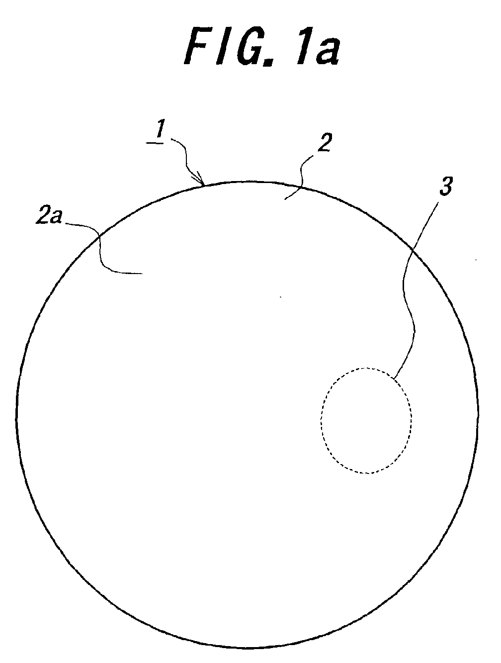
- FIG. 1(a) is a plane view showing a position of the heat spot 3 on the ceramic heater 1
- FIG 1(b) is a plane view of the ceramic heater 1A after fabricating the embossed portions as viewed from a side of a heating surface 2a.
- a substrate 2 of the ceramic heater 1A is, for example, a disk, and one of main faces of the substrate 2 constitute the heating surface 2a.
- the heat spot 3 occurs on the heating surface 2a at a target temperature.
- the target temperature herein means a maximum temperature to be reached during a treatment of the object.
- the embossed portions 4 are arranged to place the heat spot 3 in the void spaces 5 and 5A between the embossed portions.
- the number of the embossed portions per unit area on the heat spot is set to be less than that on the rest of the heating surface.
- a ratio of (the number of the embossed portions per unit area on the heat spot)/(the number of the embossed portions per unit area on the rest of the heating surface) is preferably less than 1/3 to acquire the effect of the present invention.
- the embossed portions are arranged to place the heat spot in the void space between the embossed portions, while no embossed portion is provided on the heat spot.
- the heating element is buried in a planar form in the substrate.
- the heating element is projected on the heating surface in a direction perpendicular to the heating surface, the embossed portions are fabricated on void spaces of the heating element.
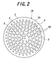
- FIG. 2 shows a heater representing this embodiment.
- the embossed portions 4 are arranged not to be above the heating element 6 on the heating surface 2a. That is, when the heating element 6 is projected on the heating surface in a direction perpendicular to the heating surface, no embossed portion exists on an area in which the heating element 6 exist, while the area in which the heating element 6 exists is located on the spaces 5B between the embossed portions.
- the number of the embossed portions per unit area above the heating element is set to be less than that on the rest of the heating surface.
- a ratio of (the number of the embossed portions per unit area above the heating element)/(the number of the embossed portions per unit area on the rest of the heating surface) is preferably less than 1/3 to acquire the effect of the present invention.
- the embossed portions are arranged to place the heating element in the void space between the embossed portions, while no embossed portion is provided above the heating element.
- a plurality of heating elements are buried in the substrate.
- Each of the heating elements is buried along each of respectively corresponding planes.
- the heating elements are projected on the heating surface in a direction perpendicular to the heating surface, they overlap each other to exist nearly in the same position.
- the ceramic heater 1D shown in FIG. 3 represents the above embodiment.
- a plurality of, for example, two lines of heating elements 6A and 6B are buried in the substrate 2.
- Each of the heating elements 6A and 6B is buried in the substrate to stretch along a plane A or B, respectively, which planes are parallel to each other.
- Each of the heating elements 6A and 6B is connected to an electric power source 11 or 12 via a terminal 9 or 10, respectively.
- FIG. 4 is a plane view of the substrate 2 as viewed from the side of the heating surface 2a showing a two-dimensional pattern of the heating element 6A with a dotted line.
- the dotted line is a patter of the heating element 6A when the heating element 6A is projected on the heating surface 2a in a direction C perpendicular to the heating surface 2a.
- the embossed portions 4 are not fabricated on the area in which the heating element 6A exists.
- the area in which the projected heating element 6A exists is located on the space 5B between the embossed portions 4.
- FIG. 5 is a plane view of the substrate 2 as viewed from the side of the heating surface 2a showing a two-dimensional pattern of the heating element 6B with a dotted line.
- the dotted line is a pattern of the heating element 6B when the heating element 6A is projected on the heating surface 2a in a direction C perpendicular to the heating surface 2a.
- the embossed portions 4 are not fabricated on the area in which the projected heating element 6B exists.
- the area in which the projected heating element 6B exists is located on the space 5B between the embossed portions 4.
- the projected heating elements 6A and 6B overlap each other to exist nearly in the same position.
- the embossed portions 4 do not exist on the area of the heating surface 2a in which the projected heating element 6A or 6B exists. That is, the area in which each of the projected heating elements 6A and 6B exists is placed on space 5B between the embossed portions.
- a plurality of heating elements are buried in the substrate.
- Each of the heating elements is buried along each of respectively corresponding planes.
- the heating elements are projected on the heating surface in a direction perpendicular to the heating surface, they exist in mutually different positions (positions without overlapping).
- the embossed portions are fabricated on the space of the heating surface between each of the heat spot since the heat spot appear on the heating surface along shapes corresponding to each of the buried heating elements.
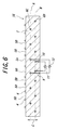
- the ceramic heater 1E shown in FIG. 6 represents the above embodiment.
- a plurality of, for example, two lines of heating elements 6C and 6D are buried in the substrate 2.
- Each of the heating elements 6C and 6D is buried in the substrate to stretch along a plane A or B, respectively, which planes are parallel to each other.
- Each of the heating elements 6C and 6D is connected to an electric power source 11 or 12 via a terminal 9 or 10, respectively.
- the projected heating elements 6C and 6D exist in mutually different positions (positions without overlapping) on the heating surface 2a.
- the embossed portion do not exist on the area of the heating surface 2a in which the projected heating element 6C or 6D exists, and the area in which each of the projected heating elements 6C and 6D exists is located on the space 5D between the embossed portions.
- a height of each of the embossed portions 4 is preferably 5 - 500 ⁇ m from the standpoint of inhibiting an effect of the heat spot on the objects.
- the diameter ⁇ of each of the embossed portions is preferably 0.2 - 10 mm from the standpoint of a uniform temperature distribution of the object.
- each of the embossed portions may be varied in a two-dimensional shape and a two-dimensional size.
- a shape of a surface of the embossed portions which are to contact with the object may be polygonal such as triangle, tetragonal or hexagonal, ring or strip.
- the number of the embossed portions is not particularly restricted. However, 0.0025 - 0.32 pieces/mm 2 is the particularly preferred number of the embossed portions per unit area from the standpoint of ensuring a uniform suction force against the object, especially against a substrate for manufacturing a semiconductor wafer or a semiconductor of a LCD panel, throughout the surface of the object.
- each of the embossed portions is measured with a dial gauge or a three-dimensional shape-measuring device.
- a material of the ceramic heater 2 is not restricted, an aluminum nitride base ceramic, a composite material containing aluminum nitride, an alumina base ceramic, a composite material containing alumina, and a composite ceramic of alumina and aluminum nitride are preferred from the standpoint of further reducing a generation of particle.
- a material of the embossed portions is not particularly restricted, but an aluminum nitride base ceramic, a composite material containing aluminum nitride, an alumina base ceramic, a composite material containing alumina, and a composite ceramic of alumina and aluminum nitride are preferred from the standpoint of further reducing a generation of particle.
- the embossed portions are fabricated with a blast process, a CVD process or the like.
- a material of the heating element is also not restricted.
- a conductive ceramic or a metal may be used, and preferably a high-melting point metal, and more preferably molybdenum, tungsten and an alloy thereof may be used.
- a hollow space can be provided between the heating surface and the heating element in the substrate of the ceramic heater and a plurality of heat conductors can be provided in the space to transverse the space. It had not been known that the heat conduction is facilitated by providing heat conductors at some areas in the air gap, as well as the heat conduction in the substrate is inhibited by forming the air gap in the substrate, thereby inhibiting the generation of the heat spot.
- the ceramic heater is designed so that the heat conductors are arranged in the space between the heat spot and are not located on the heat spot when the heat conductors and the heat spot are projected on the heating surface in a direction perpendicular to the heating surface.
- the number of the heat conductors per unit area on the heat spot is less than that on the rest of the heating surface.
- a ratio of (the number of the heat conductors per unit area on the heat spot)/(the number of the heat conductors per unit area on the rest of the heating surface) is preferably less than 1/3 to acquire the effect of the present invention.
- the heating elements are buried in planar forms in the substrate, and the heat conductors are formed in the space between the heating elements when the heat conductors and the heating elements are projected on the heating surface in a direction perpendicular to the heating surface.
- FIGS. 7(a) and (b) show the ceramic heater 1C representing the above embodiment.
- FIG. 7(a) is a cross-sectional view of the ceramic heater 1C
- FIG. 7(b) is a vertical-sectional view of the ceramic heater 1C.
- a laterally extending space 7 is formed in the substrate 12 of the ceramic heater 1C.
- the substrate 12 is divided into a supporting portion 12a and a surface layer portion 12b by the space 7.
- the heating element 6 is formed in the supporting portion 12a.
- the heating surface 12c is provided on the surface layer portion 12b.
- the heat conductors 14 are formed at given places in the space 7, and the supporting portion 12a and the surface layer portion 12b are connected via the heat conductors 14.
- a peripheral joint portion 12d is provided at a peripheral side face of the substrate 12, and the supporting portion 12a and the surface layer portion 12b are joined by the peripheral joint portion 12d.
- the heating element 6 is buried along a plane D in the substrate 12. In FIG. 7(a), the heating element 6 is shown with dotted line.
- the heat conductors 14 are formed in the space of the heating element when the heat conductors 14 and the heating element 6 are projected on the heating surface 12c in a direction perpendicular to the heating surface 12c.
- a plurality of the heating elements are buried in the substrate.
- Each of the heating elements is buried along each of respectively corresponding planes.
- the heating elements are projected on the heating surface in a direction perpendicular to the heating surface, they overlap each other to exist nearly in the same position. In this case, since the heat spot occur at the same area on the heating surface as each of the projected heating elements exists, a heat conduction in the substrate is inhibited by avoiding the areas from existing the heat conductors.
- a plurality of the heating elements are buried in the substrate.
- Each of the heating elements is buried along each of respectively corresponding planes.
- the heating elements are projected on the heating surface in a direction perpendicular to the heating surface, they exist in mutually different positions (positions without overlapping). In this case, the mutually independent heat spots corresponding to each of the heating elements occur at mutually independent positions. Therefore, the heat conduction in the substrate is inhibited by avoiding the areas from existing the heat conductors.
- the pressure in the space is particularly preferably set to not more than 3 torr. This inhibits convective heat conduction in the space to give radiant heat conduction as a dominant condition, so the heat spot can be effectively prevented.
- a material of the heat conductors is not particularly restricted, but preferably the same material as that of the substrate.
- Aluminum nitride base ceramic, a composite material containing aluminum nitride, alumina base ceramic, a composite material containing alumina, and a composite ceramic of alumina and aluminum nitride are preferred for the material.
- Ceramic heaters schematically shown in FIGS. 3-5 were manufactured. Specifically, aluminum nitride powder obtained by a reduction nitriding process were used, an acrylic resin binder was added therein, and then the mixture was granulated by a spray dryer, thereby obtaining granulated grains. Three sheets of molded bodies were sequentially made by uniaxially press-molding the granulated grains, and then each of the three layers of molded bodies was stacked on top of another to make them a single piece. Coil-like resistance-heating elements 6A and 6B made of molybdenum were buried in the uniaxially press-molded body.
- the molded body was placed in a hot press mold, which was hermetically sealed.
- the molded body was heated at a heating rate of 300°C/hr. while the pressure was reduced in a temperature range from the room temperature to 1,000°C. After the temperature reached at 1,000°C, the pressure was simultaneously increased with increase in the temperature.
- the maximum temperature was 1,800°C, and the molded body was held and fired at the maximum temperature under 200kgf/cm 2 for 4 hours in nitrogen gas to obtain a sintered body. Then the sintered body was subjected to a machine work and a finish machining, thereby a heater was prepared.
- the diameter and the thickness of a substrate 2 were set to 240mm and 18mm, respectively.
- the clearance between the resistance-heating elements 6A and 6B was set to 5.5mm.
- the surface of the substrate 2 was sandblasted to fabricate the embossed portions 4.
- the height, the diameter and the density of the embossed portions 4 were set to 20 ⁇ m, 3 mm and 1.5 pieces/cm 2 , respectively.
- the average temperature of the heating surface of the heating apparatus was set to about 650°C by controlling power supply from each AC power source.
- the pressures in the chamber were set to high vacuum, 3 torr, 30 torr and 50 torr.
- the semiconductor film was made of, for example, TiN, SiO 2 , low-K material, Si 3 N 4 , Ta 2 O 3 or the like, and was used as a metal wiring film, insulating film, barrier film, electrode, capacitor, or the like. A surface state of the thus obtained silicon surface was observed.
- the pressure in the chamber was high vacuum or 3 torr, a pattern of the semiconductor film corresponding to the heating elements was not observed at all.
- the pressure was 30 torr or 50 torr, a pattern of the semiconductor film corresponding to the heating elements was observed in some degree.
- a further detailed investigation was conducted, and a thickness distribution was measured between the adjacent patterns to give a variation of not more than 1%. This level was not more than a half of the film thickness distribution over the entire wafer, so it is practically not a problem.
- Ceramic heaters were manufactured and patterns on the semiconductor film were observed in the same manner as Experiment 1 except that the heating elements 6A and 6B having patterns shown in FIGS. 4 and 5 were used.
- the embossed portions on the heating surface were arranged in a completely random pattern so that the embossed portions were located above the heating elements also.
- the space 7 and the heat conductors 14 having shapes shown in FIGS. 7(a) and (b) were used.
- the heat conductors 14 were also made of aluminum nitride.
- the thickness and the diameter of the space 7 were set to 2mm and 210mm, respectively, and the diameter of the heat conductors 14 was set to 6mm.
- Each pressure in the chamber was set to high vacuum, 3 torr, 30 torr, 50 torr and 150 torr.
- Experiment 2 was repeated except that the space 7 and the conductors 14 were not provided.
- the pressure in the chamber at the time of measuring was set to high vacuum, 3 torr, 30 torr, 50 torr and 150 torr.
- a ceramic heater comprising a ceramic substrate having a heating surface for supporting and heating an object to be processed, a heating element provided in the substrate, and embossed portions on the heating surface which are to contact with the objects is provided, thereby preventing an adverse effect on the objects caused by a heat spot on the heating surface.
- the present invention also consists in use of the ceramic heaters of the present invention in production of semiconductor devices, and in semiconductor device production apparatus including a ceramic heater in accordance with the invention.
Landscapes
- Chemical & Material Sciences (AREA)
- Engineering & Computer Science (AREA)
- Ceramic Engineering (AREA)
- Inorganic Chemistry (AREA)
- Resistance Heating (AREA)
- Surface Heating Bodies (AREA)
- Container, Conveyance, Adherence, Positioning, Of Wafer (AREA)
Abstract
Description
Claims (10)
- A ceramic heater comprising a ceramic substrate having a heating surface for supporting and heating an object to be processed, a heating element provided in the substrate, and embossed portions on the heating surface which are to contact with the object, wherein a heat spot having a relatively high surface temperature will exist on the heating surface and the number of the embossed portions per unit area on the heat spot is less than that on the rest of the heating surface when an average temperature of the heating surface is raised to reach a target temperature.
- A ceramic heater comprising a ceramic substrate having a heating surface for supporting and heating an object to be processed, a heating element provided in the substrate, and embossed portions on the heating surface which are to contact with the objects, wherein the heating element is provided in a planar form in the substrate and when the embossed portions are projected on the heating surface in a direction perpendicular to the heating surface, the number of the embossed portions per unit area on the heating element is less than that on the rest of the heating surface.
- A ceramic heater as claimed in Claim 2, wherein a plurality of said heating elements are buried in said substrate, each of said heating elements is buried along each of respectively corresponding planes, and when said heating elements are projected on said heating surface in a direction perpendicular to said heating surface, said projected heating elements overlap each other to exist nearly in the same position.
- A ceramic heater as claimed in Claim 2, wherein a plurality of said heating elements are buried in said substrate, each of said heating elements is buried along each of respectively corresponding planes and when said heating elements are projected on said heating surface in a direction perpendicular to said heating surface, said projected heating elements exist in mutually different areas.
- A ceramic heater comprising a ceramic substrate having a heating surface for supporting and heating an object to be processed, and a heating element provided in the substrate, wherein a hollow space is provided between the heating surface and the heating element in the substrate and a plurality of heat conductors are provided in the space to transverse the space.
- A ceramic heater as claimed in Claim 5, wherein if said space does not exist in said substrate and the average temperature of said heating surface is raised to reach the target temperature, a heat spot having a relatively high surface temperature would exist on said heating surface, and when said heat conductors and the heat spot are projected on said heating surface in a direction perpendicular to said heating surface, the number of the heat conductors per unit area on the projected heat spot is less than that on the rest of said heating surface.
- A ceramic heater as claimed in Claim 5 or 6, wherein said heating element is provided in a planar form in said substrate and when said heat conductors and said heating element are projected on said heating surface in a direction perpendicular to said heating surface, the number of said embossed portions per unit area on said projected heating element is less than that on the rest of said heating surface.
- A ceramic heater as claimed in Claim 7, wherein a plurality of said heating elements are buried in said substrate, each of said heating elements is buried along each of respectively corresponding planes, and when said heating elements are projected on said heating surface in a direction perpendicular to said heating surface, said projected heating elements overlap each other to exist nearly in the same position.
- A ceramic heater as claimed in Claim 7, wherein a plurality of said heating elements are buried in said substrate, each of said heating elements is buried along each of respectively corresponding planes, and when said heating elements are projected on said heating surface in a direction perpendicular to said heating surface, said projected heating elements in mutually different positions.
- A ceramic heater as claimed in any one of Claims 5 - 9, wherein the pressure in said space is not more than 3 torr.
Applications Claiming Priority (2)
| Application Number | Priority Date | Filing Date | Title |
|---|---|---|---|
| JP2000319461 | 2000-10-19 | ||
| JP2000319461A JP4328003B2 (en) | 2000-10-19 | 2000-10-19 | Ceramic heater |
Publications (3)
| Publication Number | Publication Date |
|---|---|
| EP1199741A2 true EP1199741A2 (en) | 2002-04-24 |
| EP1199741A3 EP1199741A3 (en) | 2003-04-09 |
| EP1199741B1 EP1199741B1 (en) | 2004-12-22 |
Family
ID=18797913
Family Applications (1)
| Application Number | Title | Priority Date | Filing Date |
|---|---|---|---|
| EP01308810A Expired - Lifetime EP1199741B1 (en) | 2000-10-19 | 2001-10-16 | Ceramic heater to heat wafers |
Country Status (6)
| Country | Link |
|---|---|
| US (1) | US6558158B2 (en) |
| EP (1) | EP1199741B1 (en) |
| JP (1) | JP4328003B2 (en) |
| KR (1) | KR100426111B1 (en) |
| DE (1) | DE60107919T2 (en) |
| TW (1) | TW532047B (en) |
Cited By (4)
| Publication number | Priority date | Publication date | Assignee | Title |
|---|---|---|---|---|
| WO2004032187A3 (en) * | 2002-09-19 | 2004-07-01 | Applied Materials Inc | Multi-zone resitive heater |
| NL2001466C2 (en) * | 2008-04-10 | 2009-10-13 | Konink Nl Munt N V | Authentication feature and method for manufacturing thereof. |
| CN101807515B (en) * | 1999-05-19 | 2014-04-02 | 应用材料公司 | Multi-zone resitive heater |
| WO2016050229A1 (en) * | 2014-09-29 | 2016-04-07 | Forschungszentrum Jülich GmbH | High-power heater |
Families Citing this family (33)
| Publication number | Priority date | Publication date | Assignee | Title |
|---|---|---|---|---|
| JP3982674B2 (en) * | 2001-11-19 | 2007-09-26 | 日本碍子株式会社 | Ceramic heater, method for manufacturing the same, and heating device for semiconductor manufacturing apparatus |
| JP4038409B2 (en) * | 2002-08-15 | 2008-01-23 | 日本碍子株式会社 | Heating device |
| JP3833974B2 (en) | 2002-08-21 | 2006-10-18 | 日本碍子株式会社 | Manufacturing method of heating device |
| JP3855128B2 (en) * | 2003-03-24 | 2006-12-06 | 定寧 上野 | Hot plate using metal foil heater, manufacturing method thereof, and heat treatment method of liquid crystal panel using hot plate |
| JP4330949B2 (en) * | 2003-07-01 | 2009-09-16 | 東京エレクトロン株式会社 | Plasma CVD film forming method |
| KR100749375B1 (en) * | 2003-07-01 | 2007-08-14 | 동경 엘렉트론 주식회사 | Plasma chemical vapor deposition apparatus |
| US7214055B2 (en) * | 2003-11-10 | 2007-05-08 | Zippo Manufacturing Company | Colinear burner |
| US7654821B2 (en) * | 2004-02-17 | 2010-02-02 | Zippo Manufacturing Company | Flint ignited premixed lighter |
| WO2006023706A2 (en) * | 2004-08-19 | 2006-03-02 | Tosoh Quartz, Inc. | Reinforced structural member for high temperature operations and fabrication method |
| US20060289447A1 (en) * | 2005-06-20 | 2006-12-28 | Mohamed Zakaria A | Heating chuck assembly |
| JP2007115736A (en) * | 2005-10-18 | 2007-05-10 | Sumitomo Electric Ind Ltd | Wafer heating hot plate |
| US8226769B2 (en) * | 2006-04-27 | 2012-07-24 | Applied Materials, Inc. | Substrate support with electrostatic chuck having dual temperature zones |
| US8193473B2 (en) * | 2008-02-08 | 2012-06-05 | Ngk Insulators, Ltd. | Uniform temperature heater |
| KR100963224B1 (en) * | 2009-02-03 | 2010-06-10 | (주) 더몰론코리아 | Ceramic coating heater which can be used in water and air |
| NZ602911A (en) | 2010-04-28 | 2015-01-30 | Univ Georgia | Photochemical cross-linkable polymers, methods of marking photochemical cross-linkable polymers, methods of using photochemical cross-linkable polymers, and methods of making articles containing photochemical cross-linkable polymers |
| WO2013012664A2 (en) | 2011-07-15 | 2013-01-24 | The University Of Georgia Research Foundation, Inc | Permanent attachment of agents to surfaces containing c-h functionality |
| JP5505667B2 (en) | 2011-09-30 | 2014-05-28 | Toto株式会社 | AC drive electrostatic chuck |
| WO2013056007A2 (en) | 2011-10-14 | 2013-04-18 | University Of Georgia Research Foundation, Inc. | Photochemical cross-linkable polymers, methods of making photochemical cross-linkable plolymers, methods of using photochemical cross-linkable poloymers, and methods of making articles containing photochemical cross-linkable polymers |
| JP6703872B2 (en) * | 2016-03-28 | 2020-06-03 | 日本碍子株式会社 | Heater and honeycomb structure including the heater |
| JP6704791B2 (en) * | 2016-05-25 | 2020-06-03 | 日本特殊陶業株式会社 | Heating device |
| JP6758143B2 (en) * | 2016-09-29 | 2020-09-23 | 日本特殊陶業株式会社 | Heating device |
| WO2019083045A1 (en) * | 2017-10-27 | 2019-05-02 | 京セラ株式会社 | Heater and heater system |
| JP7308254B2 (en) * | 2018-02-19 | 2023-07-13 | 日本特殊陶業株式会社 | holding device |
| JP7164979B2 (en) * | 2018-07-02 | 2022-11-02 | 日本特殊陶業株式会社 | electrostatic chuck |
| KR102608397B1 (en) * | 2018-10-16 | 2023-12-01 | 주식회사 미코세라믹스 | Middle zone independent control ceramic heater |
| US12575369B2 (en) | 2021-03-30 | 2026-03-10 | Niterra Co., Ltd. | Electrode-embedded member with pin-shaped projections of varying heights, substrate holding member, ceramic heater, and electrostatic chuck |
| JP7748280B2 (en) * | 2021-03-30 | 2025-10-02 | 日本特殊陶業株式会社 | Electrode embedding member, substrate holding member, ceramic heater, and electrostatic chuck |
| KR102658726B1 (en) * | 2021-12-03 | 2024-04-18 | 주식회사 케이에스엠컴포넌트 | Heating device for semiconductor manufacturing equipment |
| JP2024021864A (en) * | 2022-08-04 | 2024-02-16 | 日本特殊陶業株式会社 | ceramic heater |
| JP2024038621A (en) * | 2022-09-08 | 2024-03-21 | 日本特殊陶業株式会社 | ceramic heater |
| KR20240159472A (en) | 2023-04-28 | 2024-11-05 | 니혼도꾸슈도교 가부시키가이샤 | Ceramic heater |
| KR20240170404A (en) | 2023-05-26 | 2024-12-03 | 니혼도꾸슈도교 가부시키가이샤 | Ceramic heater |
| KR102789129B1 (en) * | 2023-12-28 | 2025-04-03 | 주식회사 미코세라믹스 | Ceramic Susceptor |
Family Cites Families (15)
| Publication number | Priority date | Publication date | Assignee | Title |
|---|---|---|---|---|
| US4518848A (en) * | 1981-05-15 | 1985-05-21 | Gca Corporation | Apparatus for baking resist on semiconductor wafers |
| JPS6452065A (en) * | 1987-08-21 | 1989-02-28 | Matsushita Electric Industrial Co Ltd | Sputtering target |
| JPH0724796Y2 (en) * | 1990-02-13 | 1995-06-05 | 日新電機株式会社 | High temperature plate heater |
| JPH05326112A (en) * | 1992-05-21 | 1993-12-10 | Shin Etsu Chem Co Ltd | Layered ceramic heater |
| JPH0786247A (en) | 1993-09-16 | 1995-03-31 | Hitachi Ltd | METHOD AND APPARATUS FOR TREATING OBJECT TO BE PROCESSED IN REDUCED AMBIENT |
| JP3234091B2 (en) | 1994-03-10 | 2001-12-04 | 株式会社日立製作所 | Surface treatment equipment |
| TW444922U (en) * | 1994-09-29 | 2001-07-01 | Tokyo Electron Ltd | Heating device and the processing device using the same |
| JPH09171953A (en) | 1995-12-20 | 1997-06-30 | Sony Corp | Substrate heating device, substrate heating method, semiconductor integrated circuit device, photomask, and liquid crystal display device |
| JPH10284360A (en) * | 1997-04-02 | 1998-10-23 | Hitachi Ltd | Substrate temperature control device and method |
| US6286451B1 (en) * | 1997-05-29 | 2001-09-11 | Applied Materials, Inc. | Dome: shape and temperature controlled surfaces |
| JPH11260534A (en) * | 1998-01-09 | 1999-09-24 | Ngk Insulators Ltd | Heating device and method of manufacturing the same |
| JP4039645B2 (en) * | 1998-01-16 | 2008-01-30 | キヤノンアネルバ株式会社 | Vacuum processing equipment |
| JP3631614B2 (en) * | 1998-05-29 | 2005-03-23 | 京セラ株式会社 | Ceramic heater |
| JP3983387B2 (en) * | 1998-09-29 | 2007-09-26 | 日本碍子株式会社 | Electrostatic chuck |
| JP3844408B2 (en) * | 1999-01-26 | 2006-11-15 | 信越化学工業株式会社 | Multilayer ceramic heater |
-
2000
- 2000-10-19 JP JP2000319461A patent/JP4328003B2/en not_active Expired - Lifetime
-
2001
- 2001-07-25 TW TW090118157A patent/TW532047B/en not_active IP Right Cessation
- 2001-10-12 US US09/976,464 patent/US6558158B2/en not_active Expired - Lifetime
- 2001-10-12 KR KR1020010062904A patent/KR100426111B1/en not_active Expired - Lifetime
- 2001-10-16 EP EP01308810A patent/EP1199741B1/en not_active Expired - Lifetime
- 2001-10-16 DE DE60107919T patent/DE60107919T2/en not_active Expired - Lifetime
Cited By (5)
| Publication number | Priority date | Publication date | Assignee | Title |
|---|---|---|---|---|
| CN101807515B (en) * | 1999-05-19 | 2014-04-02 | 应用材料公司 | Multi-zone resitive heater |
| WO2004032187A3 (en) * | 2002-09-19 | 2004-07-01 | Applied Materials Inc | Multi-zone resitive heater |
| NL2001466C2 (en) * | 2008-04-10 | 2009-10-13 | Konink Nl Munt N V | Authentication feature and method for manufacturing thereof. |
| WO2009126030A1 (en) * | 2008-04-10 | 2009-10-15 | Koninklijke Nederlandse Munt N.V. | Authentication feature and method for its production |
| WO2016050229A1 (en) * | 2014-09-29 | 2016-04-07 | Forschungszentrum Jülich GmbH | High-power heater |
Also Published As
| Publication number | Publication date |
|---|---|
| EP1199741A3 (en) | 2003-04-09 |
| DE60107919D1 (en) | 2005-01-27 |
| KR100426111B1 (en) | 2004-04-08 |
| EP1199741B1 (en) | 2004-12-22 |
| KR20020033407A (en) | 2002-05-06 |
| JP2002124367A (en) | 2002-04-26 |
| JP4328003B2 (en) | 2009-09-09 |
| US20020102512A1 (en) | 2002-08-01 |
| TW532047B (en) | 2003-05-11 |
| US6558158B2 (en) | 2003-05-06 |
| DE60107919T2 (en) | 2005-12-08 |
Similar Documents
| Publication | Publication Date | Title |
|---|---|---|
| US6558158B2 (en) | Ceramic heater | |
| JP3567855B2 (en) | Wafer holder for semiconductor manufacturing equipment | |
| KR100420456B1 (en) | Wafer holder for semiconductor manufacturing apparatus, method of manufacturing wafer holder, and semiconductor manufacturing apparatus | |
| US7275309B2 (en) | Method of manufacturing electrical resistance heating element | |
| KR100672802B1 (en) | Substrate heating device and manufacturing method thereof | |
| EP1119025A2 (en) | Wafer holder for semiconductor manufacturing apparatus | |
| US7060945B2 (en) | Substrate heater and fabrication method for the same | |
| KR20190142384A (en) | Wafer support | |
| JPH11260534A (en) | Heating device and method of manufacturing the same | |
| KR20010078235A (en) | Heating apparatus | |
| JP2003151729A (en) | Ceramic heater, method of manufacturing the same, and heating device for semiconductor manufacturing equipment | |
| KR100709536B1 (en) | Systems for heating wafers | |
| JP2006127900A (en) | Annular heater | |
| JP4566213B2 (en) | Heating apparatus and manufacturing method thereof | |
| JP4529690B2 (en) | Wafer holder for semiconductor manufacturing apparatus, manufacturing method thereof, and semiconductor manufacturing apparatus | |
| JPH07153820A (en) | Susceptor for semiconductor manufacturing and manufacturing method thereof | |
| US20250176074A1 (en) | Ceramic heater | |
| TW202531459A (en) | Ceramic base | |
| JP4325083B2 (en) | Ceramic heater unit for semiconductor manufacturing apparatus and semiconductor manufacturing apparatus | |
| JPH06260263A (en) | Ceramic heater manufacturing method | |
| JP2025004713A (en) | Ceramic Susceptor |
Legal Events
| Date | Code | Title | Description |
|---|---|---|---|
| PUAI | Public reference made under article 153(3) epc to a published international application that has entered the european phase |
Free format text: ORIGINAL CODE: 0009012 |
|
| AK | Designated contracting states |
Kind code of ref document: A2 Designated state(s): AT BE CH CY DE DK ES FI FR GB GR IE IT LI LU MC NL PT SE TR |
|
| AX | Request for extension of the european patent |
Free format text: AL;LT;LV;MK;RO;SI |
|
| PUAL | Search report despatched |
Free format text: ORIGINAL CODE: 0009013 |
|
| AK | Designated contracting states |
Kind code of ref document: A3 Designated state(s): AT BE CH CY DE DK ES FI FR GB GR IE IT LI LU MC NL PT SE TR Designated state(s): AT BE CH CY DE DK ES FI FR GB GR IE IT LI LU MC NL PT SE TR |
|
| AX | Request for extension of the european patent |
Extension state: AL LT LV MK RO SI |
|
| 17P | Request for examination filed |
Effective date: 20030922 |
|
| 17Q | First examination report despatched |
Effective date: 20031106 |
|
| AKX | Designation fees paid |
Designated state(s): DE FR GB |
|
| GRAP | Despatch of communication of intention to grant a patent |
Free format text: ORIGINAL CODE: EPIDOSNIGR1 |
|
| GRAS | Grant fee paid |
Free format text: ORIGINAL CODE: EPIDOSNIGR3 |
|
| GRAA | (expected) grant |
Free format text: ORIGINAL CODE: 0009210 |
|
| AK | Designated contracting states |
Kind code of ref document: B1 Designated state(s): DE FR GB |
|
| REG | Reference to a national code |
Ref country code: GB Ref legal event code: FG4D |
|
| REG | Reference to a national code |
Ref country code: IE Ref legal event code: FG4D |
|
| REF | Corresponds to: |
Ref document number: 60107919 Country of ref document: DE Date of ref document: 20050127 Kind code of ref document: P |
|
| ET | Fr: translation filed | ||
| PLBE | No opposition filed within time limit |
Free format text: ORIGINAL CODE: 0009261 |
|
| STAA | Information on the status of an ep patent application or granted ep patent |
Free format text: STATUS: NO OPPOSITION FILED WITHIN TIME LIMIT |
|
| 26N | No opposition filed |
Effective date: 20050923 |
|
| REG | Reference to a national code |
Ref country code: FR Ref legal event code: PLFP Year of fee payment: 16 |
|
| REG | Reference to a national code |
Ref country code: FR Ref legal event code: PLFP Year of fee payment: 17 |
|
| REG | Reference to a national code |
Ref country code: FR Ref legal event code: PLFP Year of fee payment: 18 |
|
| PGFP | Annual fee paid to national office [announced via postgrant information from national office to epo] |
Ref country code: FR Payment date: 20200914 Year of fee payment: 20 |
|
| PGFP | Annual fee paid to national office [announced via postgrant information from national office to epo] |
Ref country code: GB Payment date: 20201007 Year of fee payment: 20 Ref country code: DE Payment date: 20201006 Year of fee payment: 20 |
|
| REG | Reference to a national code |
Ref country code: DE Ref legal event code: R071 Ref document number: 60107919 Country of ref document: DE |
|
| REG | Reference to a national code |
Ref country code: GB Ref legal event code: PE20 Expiry date: 20211015 |
|
| PG25 | Lapsed in a contracting state [announced via postgrant information from national office to epo] |
Ref country code: GB Free format text: LAPSE BECAUSE OF EXPIRATION OF PROTECTION Effective date: 20211015 |