The present invention relates to a photovoltaic
module and to the manufacturing method thereof, and in
particular, to a photovoltaic module including hybrid-type
photovoltaic cells each provided with a conductive
interlayer having a light-transmitting-and-reflecting
property, and to the manufacturing method thereof.
The photovoltaic module generally has a structure
in which a plurality of photovoltaic cells are arrayed
in series on a glass substrate. These photovoltaic
cells are respectively formed through the depositions
on the glass substrate and patterning, of a transparent
front electrode, a photovoltaic layer and a back
electrode.
This photovoltaic module is demanded to be
excellent in conversion efficiency of light to electric
power (or power generating efficiency). A module
including tandem-type photovoltaic cells, i.e. a
tandem-type module has a structure in which a laminate
structure of photovoltaic layers differing in
absorption band of wavelength from each other
intervenes between the front electrode and the back
electrode, and is known to be capable of more
effectively utilizing the incident light.
A hybrid-type structure which is one kind of
tandem-type structure is featured in that the
photovoltaic layers are different to each other in
crystallinity of intrinsic semiconductor layer which
constitutes a main portion of each photovoltaic layer.
For example, a module having hybrid-type cells, i.e.
a hybrid-type module employs, as the intrinsic semiconductor
layer of the photovoltaic layer disposed on
the incident light side (or front side), an amorphous
silicon layer having a wider band gap, and also
employs, as the intrinsic semiconductor layer of
the photovoltaic layer disposed on the rear side,
a polysilicon layer having a narrower band gap.
By the way, there is a kind of tandem-type module
wherein a conductive interlayer exhibiting a light-transmitting-and-reflecting
properties is interposed
between a plurality of photovoltaic layers being
laminated. Since it is possible, with this interlayer
being provided as mentioned above, to enable the light
entered into the intrinsic semiconductor layer disposed
on the front side to be reflected by this interlayer,
the effective thickness of the intrinsic semiconductor
layer disposed on the front side can be increased, or
in other words, the density of output current of the
photovoltaic layer disposed on the front side can be
increased.
Therefore, if this interlayer is applied to the
aforementioned hybrid-type cell, the density of output
current may be well-balanced between the photovoltaic
layer having an amorphous silicon layer and the
photovoltaic layer having a polysilicon layer while
making it possible to make thinner the amorphous
silicon layer which may be increasingly photo-induced
degraded as the thickness thereof is increased.
Namely, the output performance of the module is assumed
to be improved.
However, as a matter of fact, it is not
necessarily possible, in the hybrid-type module which
is provided with the aforementioned interlayer, to
realize such an improved output performance as
expected.
An object of the present invention is to realize
a high output performance in a photovoltaic module
including hybrid-type photovoltaic cells each provided
with a conductive interlayer with a light-transmitting-and-reflecting
property.
According to a first aspect of the present
invention, there is provided a photovoltaic module
comprising a transparent substrate and hybrid-type
photovoltaic cells arrayed on the substrate and series
connected to each other, the cells comprising a back
electrode facing the substrate, a transparent front
electrode intervening between the substrate and the
back electrode, a first photovoltaic layer intervening
between the front and back electrodes and comprising
an amorphous semiconductor layer, a second photovoltaic
layer intervening between the first photovoltaic layer
and the back electrode and comprising a crystalline
semiconductor layer, and a conductive interlayer with a
light-transmitting-and-reflecting property intervening
between the first and second photovoltaic layers and
having a thickness in a range of 10 nm to 100 nm and
a specific resistance in a range of 1 × 10⁻³ Ω·cm to
1 × 10⁻¹ Ω·cm.
According to a second aspect of the present
invention, there is provided a photovoltaic module
comprising a transparent substrate and hybrid-type
photovoltaic cells arrayed on the substrate and series
connected to each other, the cells comprising a back
electrode facing the substrate, a transparent front
electrode intervening between the substrate and the
back electrode, a first photovoltaic layer intervening
between the front and back electrodes and comprising
an amorphous semiconductor layer, a second photovoltaic
layer intervening between the first photovoltaic layer
and the back electrode and comprising a crystalline
semiconductor layer, and a conductive interlayer with a
light-transmitting-and-reflecting property intervening
between the first and second photovoltaic layers,
wherein, between each two of the cells adjacent to
each other, the front electrode is divided by a first
separation groove which is filled with a material of
the first photovoltaic layer, a laminate structure
comprising the first photovoltaic layer, the
interlayer, the second photovoltaic layer and the back
electrode is divided by a second separation groove
which is apart from the first separation groove, a
laminate structure comprising the first photovoltaic
layer, the interlayer and the second photovoltaic layer
is divided by a connection groove between the first and
second separation grooves, the connection groove being
filled with a material of the back electrode so as to
electrically connect the back electrode of one of the
two cells to the front electrode of the other of the
two cells, and a laminate structure comprising the
first photovoltaic layer and the interlayer is divided
by a third separation groove which is filled with
a material of the second photovoltaic layer, the
connection groove being positioned between the second
and third grooves, and the first and third grooves
being apart from each other.
According to a third aspect of the present
invention, there is provided a photovoltaic module
comprising a transparent substrate and hybrid-type
photovoltaic cells arrayed on the substrate and series
connected to each other, the cells comprising a back
electrode facing the substrate, a transparent front
electrode intervening between the substrate and the
back electrode, a first photovoltaic layer intervening
between the front and back electrodes and comprising
an amorphous semiconductor layer, a second photovoltaic
layer intervening between the first photovoltaic layer
and the back electrode and comprising a crystalline
semiconductor layer, and a conductive interlayer with a
light-transmitting-and-reflecting property intervening
between the first and second photovoltaic layers,
wherein, between each two of the cells adjacent to each
other, the front electrode is divided by first and
fourth grooves which are apart from each other and
filled with a material of the first photovoltaic layer,
a laminate structure comprising the first photovoltaic
layer, the interlayer, the second photovoltaic layer
and the back electrode is divided by a second
separation groove, the second and first separation
grooves sandwiching the fourth groove, a laminate
structure comprising the first photovoltaic layer,
the interlayer and the second photovoltaic layer is
divided by a connection groove between the fourth and
second separation grooves, the connection groove being
filled with a material of the back electrode so as to
electrically connect the back electrode of one of the
two cells to the front electrode of the other of the
two cells, and a laminate structure comprising the
first photovoltaic layer and the interlayer is divided
by a third separation groove which is filled with
a material of the second photovoltaic layer and
positioned between the first and fourth grooves.
According to a fourth aspect of the present
invention, there is provided a photovoltaic module
comprising a transparent substrate and hybrid-type
photovoltaic cells arrayed on the substrate and series
connected to each other, the cells comprising a back
electrode facing the substrate, a transparent front
electrode intervening between the substrate and the
back electrode, a first photovoltaic layer intervening
between the front and back electrodes and comprising
an amorphous semiconductor layer, a second photovoltaic
layer intervening between the first photovoltaic layer
and the back electrode and comprising a crystalline
semiconductor layer, and a conductive interlayer with a
light-transmitting-and-reflecting property intervening
between the first and second photovoltaic layers,
wherein, between each two of the cells adjacent to
each other, the front electrode is divided by a first
separation groove which is filled with a material of
the first photovoltaic layer, a laminate structure
comprising the first photovoltaic layer, the
interlayer, the second photovoltaic layer and the back
electrode is divided by a second separation groove
which is apart from the first separation groove,
a laminate structure comprising the first photovoltaic
layer, the interlayer and the second photovoltaic layer
is divided by a connection groove between the first and
second separation grooves, the connection groove being
filled with a material of the back electrode so as to
electrically connect the back electrode of one of the
two cells to the front electrode of the other of the
two cells, and a laminate structure comprising the
front electrode, the first photovoltaic layer and the
interlayer is divided by a third separation groove
which is filled with a material of the second
photovoltaic layer, the connection groove being
positioned between the second and third grooves, and
the first and third grooves being apart from each
other.
According to a fifth aspect of the present
invention, there is provided a photovoltaic module
comprising a transparent substrate and hybrid-type
photovoltaic cells arrayed on the substrate and series
connected to each other, the cells comprising a back
electrode facing the substrate, a transparent front
electrode intervening between the substrate and the
back electrode, a first photovoltaic layer intervening
between the front and back electrodes and comprising
an amorphous semiconductor layer, a second photovoltaic
layer intervening between the first photovoltaic layer
and the back electrode and comprising a crystalline
semiconductor layer, and a conductive interlayer with a
light-transmitting-and-reflecting property intervening
between the first and second photovoltaic layers,
wherein, between each two of the cells adjacent to
each other, a laminate structure comprising the front
electrode, the first photovoltaic layer and the
interlayer is divided by a first separation groove
which is filled with a material of the second
photovoltaic layer, a laminate structure comprising the
first photovoltaic layer, the interlayer, the second
photovoltaic layer and the back electrode is divided by
a second separation groove which is apart from the
first separation groove, and a laminate structure
comprising the first photovoltaic layer, the interlayer
and the second photovoltaic layer is divided by
a connection groove between the first and second
separation grooves, the connection groove bordering
on the first separation groove and being filled with
a material of the back electrode so as to electrically
connect the back electrode of one of the two cells to
the front electrode of the other of the two cells.
According to a sixth aspect of the present
invention, there is provided a method of manufacturing
a photovoltaic module, which comprises a transparent
substrate and hybrid-type photovoltaic cells arrayed
on the substrate and series connected to each other,
comprising forming a transparent front electrode on
the substrate, forming a first photovoltaic layer
comprising an amorphous semiconductor layer on the
front electrode, forming a conductive interlayer with
a light-transmitting-and-reflecting property on the
first photovoltaic layer, forming a separation groove
which divides a laminate structure comprising the first
photovoltaic layer and the interlayer, subjecting the
laminate structure to an etching treatment so as to
dissolve electrically conductive particles and form
a textured pattern on a surface of the interlayer,
the particles resulting from the formation of the
separation groove and being attached to a sidewall of
the separation groove, forming a second photovoltaic
layer comprising a crystalline semiconductor layer on
the interlayer after the etching treatment, and forming
a back electrode on the second photovoltaic layer.
The term "crystalline" employed herein is meant to
include "polycrystalline" and also "microcrystalline".
Further, these "polycrystalline" and "microcrystalline"
may contain therein an "amorphous".
This summary of the invention does not necessarily
describe all necessary features so that the invention
may also be a sub-combination of these described
features.
The invention can be more fully under stood from
the following detailed description when taken in
conjunction with the accompanying drawings, in which:
Several embodiments of the present invention
will be described with reference to the accompanying
drawings. By the way, the components which are common
in these drawing are denoted by the same reference
numerals thereby omitting the repeated explanation
thereof.
The present inventors have investigated as for
the reasons which make it impossible to realize such
an output performance as expected of the conventional
hybrid-type module which is provided with the
aforementioned interlayer. As a result, the following
fact has been found as being one of the main reasons.
In the tandem-type photovoltaic module, the
electric connection between the back electrode of
a given photovoltaic cell and the transparent front
electrode of another photovoltaic cell adjacent to the
given photovoltaic cell is realized by the provision
of a connection groove passing through a plurality of
photovoltaic layers as well as an interlayer interposed
therebetween, the connection groove being filled with
a material constituting the back electrode. Namely,
the conductive body filling the connection groove is in
contact with the light-reflective interlayer.
Since this interlayer is electrically conductive
as mentioned above, this interlayer functions also as
an electrode. Further, in the tandem-type photovoltaic
module, a plurality of photovoltaic layers to be
included in a single photovoltaic cell are assumed as
being connected in series with each other. Therefore,
according to the conventional module, a leak current is
caused to generate through the interlayer as well as
through the conductive material filling the connection
groove. As a result, it has been impossible to
effectively take up the electric power that has been
generated at the photovoltaic layer interposed between
the back electrode and the interlayer.
According to the following first to sixth
embodiments, however, the generation of such a leak
current can be inhibited, thereby making it possible
to achieve a high output performance.
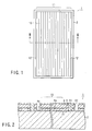
FIG. 1 is a plane view schematically showing
a photovoltaic module according to a first embodiment
of the present invention. In the photovoltaic module
shown in FIG. 1, a plurality of photovoltaic cells 10
are arrayed on a transparent substrate 2. These
photovoltaic cells 10 have stripe-like configurations
and are series-connected with each other, thereby
constructing a series array 11. A pair of bus bar
electrodes 12 each formed of ribbon-like copper foil
are attached to both ends of the series array 11.
In the followings, this module shown in FIG. 1
will be further explained in detail with reference to
FIG. 2.
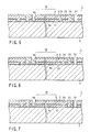
FIG. 2 is a cross-sectional view of the photovoltaic
module 1 taken along the line II-II of FIG. 1.
By the way, only part of the module 1 is depicted in
FIG. 2.
As shown in FIG. 2, the photovoltaic cells 10 of
the module 1 are respectively constructed such that
a transparent front electrode 3, a first photovoltaic
layer 4a including an amorphous semiconductor layer, an
interlayer 5, a second photovoltaic layer 4b including
a crystalline semiconductor layer, and a back electrode
6 are laminated successively on the transparent
substrate 2. Namely, this module 1 is designed such
that the incident light from the transparent substrate
2 side is converted into an electric power by means
of these photovoltaic layers 4a and 4b constituting
a hybrid-type structure.
The photovoltaic module 1 according to this
embodiment is provided with a first separation groove
21 and a second separation groove 22 both dividing the
aforementioned layers, and with a connection groove 23.
These first and second separation grooves 21 and 22 and
connection groove 23 are formed parallel with each
other and extended in the direction perpendicular to
the plane of drawings. The boundary between cells
adjacent to each other is defined by these first and
second separation grooves 21 and 22.
The first separation groove 21 divides the
transparent front electrode 3 correspondently with
each of the cells 10, and has an opening at a level of
an interface between the front electrode 3 and the
photovoltaic layer 4a, a bottom surface of the first
separation groove 21 being constituted by the surface
of the substrate 2. The first separation groove 21 is
filled with the amorphous material of the photovoltaic
layer 4a, thereby electrically insulating the adjacent
front electrodes 3 from each other.
The second separation groove 22 is formed away
from the first separation groove 21. This second
separation groove 22 divides the photovoltaic layers
4a and 4b, the interlayer 5 and the back electrode 6
correspondently with each of the cells 10, and has
an opening in the exposed surface of the back electrode
6, a bottom surface of the second separation groove 22
being constituted by the surface of the transparent
front electrode 3. This second separation groove 22
functions to electrically insulate the adjacent back
electrodes 6 from each other and also insulate the
adjacent interlayers 5 from each other at a boundary
portion between adjacent cells 10.
The connection groove 23 is formed in a position
between the first separation groove 21 and the second
separation groove 22. This connection groove 23
divides the photovoltaic layers 4a and 4b, and the
interlayer 5, and has an opening at a level of an
interface between the photovoltaic layer 4b and the
back electrode 6, a bottom surface of the connection
groove 23 being constituted by the surface of the front
electrode 3. This connection groove 23 is filled
with an electrically conductive material as the
material of the back electrode 6 such as metal,
thereby electrically connecting the back electrode 6
of one of cells 10 adjacent to each other with the
front electrode 3 of the other of the adjacent cells
10. Namely, the connection groove 23 as well as the
electrically conductive material in the connection
groove 23 function to series-connect a plurality of
cells 10 arrayed on the substrate 2 with each other.
Next, each of the constituent elements of the
aforementioned module 1 will be explained.
As for the transparent substrate 2, it is
possible to employ, for example, a glass substrate,
a transparent resin film, etc.
The transparent front electrode 3 can be
constituted by a transparent conductive oxide layer
such as an ITO film, an SnO2 film or a ZnO film.
Generally, these films are formed as a polycrystalline
film. The front electrode 3 may be a monolayer
structure or a multi-layer structure. This front
electrode 3 can be formed by means of a known vapor-phase
deposition method such as an evaporation method,
a CVD method or a sputtering method.
The surface of the front electrode 3 should
preferably be formed so as to have a surface-textured
structure including a fine roughened surface, or so-called
textured pattern. When the surface of the front
electrode 3 is provided with such a textured pattern,
the incidence efficiency of light into the photovoltaic
layer 4 can be improved. There is not any particular
limitation with respect to the method of forming the
textured pattern, and hence, various known methods can
be employed.
The photovoltaic layer 4a includes an amorphous
semiconductor layer. For example, the photovoltaic
layer 4a has a structure in which a p-type silicon-based
semiconductor layer, a silicon-based amorphous
semiconductor layer and an n-type silicon-based
semiconductor layer are successively laminated on the
front electrode 3. These p-type semiconductor layer,
amorphous semiconductor layer and n-type semiconductor
layer can be formed by means of plasma CVD method.
The photovoltaic layer 4b includes a crystalline
semiconductor layer. For example, the photovoltaic
layer 4b has a structure in which a p-type silicon-based
semiconductor layer, a silicon-based crystalline
semiconductor layer and an n-type silicon-based
semiconductor layer are successively laminated on
the interlayer 5. These p-type semiconductor layer,
crystalline semiconductor layer and n-type semiconductor
layer can be formed by means of plasma CVD
method.
The p-type semiconductor layer included in these
photovoltaic layers 4a and 4b can be formed by doping
p-type conductivity-determining impurity atoms such as
boron or aluminum into silicon or a silicon alloy such
as silicon carbide or silicon germanium. On the other
hand, the amorphous semiconductor layer and crystalline
semiconductor layer can be formed by making use of
an amorphous silicon-based semiconductor material and
a crystalline silicon-based semiconductor material,
respectively. As for the examples of such materials,
it is possible to employ an intrinsic semiconductor of
silicon (silicon hydride), or a silicon alloy such as
silicon carbide or silicon germanium. Further, a weak
p-type or weak n-type silicon-based semiconductor
material containing a trace of conductivity-determining
impurity can be employed as a material for the
amorphous semiconductor layer and crystalline
semiconductor layer as long as they are capable of
exhibiting a sufficient photoelectric conversion
characteristic. On the other hand, the n-type
semiconductor layer can be formed by doping n-type
conductivity-determining impurity atoms such as
phosphorus or nitrogen into silicon or a silicon alloy
such as silicon carbide or silicon germanium.
The photovoltaic layer 4a differs from the
photovoltaic layer 4b in terms of absorption wavelength
band. For example, when the amorphous semiconductor
layer of the photovoltaic layer 4a is formed of
an amorphous silicon layer, and the crystalline
semiconductor layer of the photovoltaic layer 4b
is formed of a crystalline silicon layer, a light
component having a wavelength of 550 nm or so can be
most effectively absorbed by the former layer, while
a light component having a wavelength of 900 nm or so
can be most effectively absorbed by the latter layer.
The thickness of photovoltaic layer 4a should
preferably be in the range of 0.01 µm to 0.5 µm,
more preferably in the range of 0.1 µm to 0.3 µm.
Since it is possible, in the module according to this
embodiment, to enable the light entered from outside
into the photovoltaic layer 4a to be reflected by
this interlayer 5, the effective thickness of the
photovoltaic layer 4a can be increased. Therefore,
it is now possible to maintain a sufficiently high
output current density even if the thickness of the
photovoltaic layer 4a is made thinner for the purpose
of inhibiting the photo-induced degradation thereof.
On the other hand, the thickness of photovoltaic
layer 4b should preferably be in the range of 0.1 µm
to 10 µm, more preferably in the range of 0.1 µm to
5 µm. Namely, the thickness of photovoltaic layer 4b
should preferably be several to ten times as large as
that of the photovoltaic layer 4a. This is because
the photo-absorption coefficient of the crystalline
semiconductor layer is smaller than that of the
amorphous semiconductor layer.
The interlayer 5 is featured in that it exhibits
light-transmitting-and-reflecting properties. Further,
the interlayer 5 is electrically conductive. As for
the specific examples of the interlayer 5, it is
possible to employ a transparent oxide layer such as
a ZnO film, an SiO2 film, an SnO2 film, an InO2 film,
an Al2O3 film, a Y2O3 film and a TiO2 film. More
preferably, a transparent conductive oxide layer such
as a ZnO film should be employed for the interlayer 5.
These films are frequently formed in the form of
polycrystal. This interlayer 5 can be formed by
a known vapor-phase deposition method such as
an evaporation method, a CVD method and a sputtering
method.
The back electrode 6 generally functions not only
as an electrode but also as a reflection layer which
permits the light that has reached the back electrode 6
after entering into the photovoltaic layers 4a and 4b
from the transparent substrate 2 to re-enter into the
photovoltaic layers 4a and 4b. This back electrode 6
can be formed to have a thickness of 200 nm to 400 nm
for instance by making use of a metallic material such
as silver or aluminum and by means of an evaporation
method or a sputtering method. This back electrode
6 may be further provided, on the surface thereof
facing the photovoltaic layer 4b, with a transparent
conductive thin film (not shown) made of a non-metallic
material such as ZnO for the purpose of improving the
adhesivity between the conductive thin film made of
a metal for example and the photovoltaic layer 4b.
The aforementioned module 1 can be manufactured by
the method explained as follows.
First of all, a transparent front electrode 3 is
formed as a continuous film on one of main surfaces
of the transparent substrate 2. Then, the first
separation groove 21 is formed in the front electrode 3
by means of a laser-scribing using YAG laser to divide
the front electrode 3 correspondently with each of the
cells 10. The electrically conductive fine particles
to be produced as a result of the laser-scribing of the
front electrode 3 are removed as required by means of
ultrasonic cleaning, etc.
Then, the photovoltaic layer 4a is formed as a
continuous film on the front electrode 3. As a result
of the formation of the photovoltaic layer 4a, the
first separation groove 21 that has been formed in the
front electrode 3 is concurrently filled with the
amorphous material constituting the photovoltaic layer
4a. Then, the interlayer 5 is formed as a continuous
film on the photovoltaic layer 4a. Thereafter, the
photovoltaic layer 4b is formed as a continuous film on
the interlayer 5.
Subsequently, the connection groove 23 is formed
in the photovoltaic layers 4a and 4b and the interlayer
5 by means of a laser-scribing using YAG laser, etc.
Then, the back electrode 6 is formed on the
photovoltaic layer 4b. As a result of the formation
of this back electrode 6, the connection groove 23 is
concurrently filled with a conductive material such
as a metal, thereby permitting the back electrode 6 to
be electrically connected with the transparent front
electrode 3 through the conductive material filling the
connection groove 23.
Then, the second separation groove 22 is formed in
the photovoltaic layers 4a and 4b, the interlayer 5,
and the back electrode 6 by means of a laser-scribing
using YAG laser, etc. Then, a power-generating region
is delimited by means of a laser-scribing using YAG
laser, etc. Further, a pair of bus bar electrodes 12
are attached to the both sides of the array constituted
by the cells 10, thus obtaining the structure as shown
in FIGS. 1 and 2.
By the way, the photovoltaic module 1 is generally
provided, on the rear side thereof, with an organic
protective film (not shown) with a sealing resin
layer (not shown) being interposed therebetween.
This sealing resin layer is designed to seal each of
the photovoltaic cells 10 formed on the transparent
substrate 2, and is formed of a resin which enables
the organic protective film to be adhered to these
cells 10.
Specific examples of such a resin includes EVA
(ethylene/vinyl acetate copolymer) for instance.
As for the organic protective film, it is possible
to employ a polyvinyl fluoride film (for example,
Tedlar film (registered trademark)). These sealing
resin/organic protective films can be concurrently
adhered to the rear side of the photovoltaic module 1
by means of vacuum laminating method.
According to this embodiment, the specific
resistance of the interlayer 5 is confined within the
range of 1 × 10⁻³Ω·cm to 1 × 10⁻¹Ω·cm, preferably
within the range of 1 × 10⁻²Ω·cm to 1 × 10⁻¹Ω·cm.
Further, this thickness of the interlayer 5 is confined
within the range of 10 nm to 100 nm, preferably within
the range of 20 nm to 70 nm. When the specific
resistance and thickness of the interlayer 5 are
confined within the aforementioned ranges, it becomes
possible to inhibit an electric current from flowing
in the direction in-plane of the interlayer 5.
Therefore, according to this embodiment, it becomes
possible to suppress the generation of leak current.
Further, when the specific resistance and thickness of
the interlayer 5 are confined within the aforementioned
ranges, it becomes possible to prevent the electric
resistance between the photovoltaic layer 4a and the
photovoltaic layer 4b from becoming excessively higher.
Additionally, when the specific resistance and
thickness of the interlayer 5 are confined within the
aforementioned ranges, the following advantages can be
obtained.
The second separation groove 22 and the connection
groove 23 can be formed by utilizing the heat and/or
kinetic energy to be generated from the fusion or
sublimation of a portion of the photovoltaic layer 4a
by the irradiation of laser beam. Therefore, if the
photovoltaic layer 4a is excessively thin, the second
separation groove 22 and the connection groove 23 may
become discontinuous, making the electric insulation or
electric connection thereof incomplete. On the other
hand, if the photovoltaic layer 4a is excessively
thick, it will lead to the photo-induced degradation
thereof. Further, since the photo-absorption
coefficient of the crystalline semiconductor layer
is smaller than that of the amorphous semiconductor
layer, the thickness of photovoltaic layer 4b should
preferably be several to ten times as large as that
of the photovoltaic layer 4a. Because of this,
the thickness of the photovoltaic layer 4a should
preferably be within the range of 0.01 µm to 0.5 µm,
more preferably within the range of 0.1 µm to 0.3 µm.
Whereas the thickness of the photovoltaic layer 4b
should preferably be within the range of 0.1 µm to
10 µm, more preferably within the range of 0.1 µm to
5 µm.
As described above, the thickness of the
interlayer 5 according to this embodiment is confined
within the range of 10 nm to 100 nm, more preferably
within the range of 20 nm to 70 nm. When the thickness
of the interlayer 5 is confined within the aforementioned
range, it becomes easy to well-balance the
output current of the photovoltaic layer 4a with the
output current of the photovoltaic layer 4b on the
occasion where the thickness of the photovoltaic layer
4a and the thickness of the photovoltaic layer 4b are
respectively confined within the aforementioned ranges.
Therefore, it is possible according to this embodiment
to easily realize excellent output performance.
According to this embodiment, the interlayer 5 may
be formed using a transparent conductive oxide such
as zinc oxide, tin oxide and indium tin oxide.
However, a transparent conductive oxide is generally
lower in oxygen concentration as compared with the
stoichiometric concentration thereof, and exhibits
an n-type conductivity. Namely, the specific
resistance of such a transparent conductive oxide
tends to become low. If it is desired to employ
a transparent conductive oxide as a material for the
interlayer 5, the transparent conductive oxide may be
doped with an impurity such as aluminum or gallium to
adjust the specific resistance of the interlayer 5.
Additionally, the oxygen concentration in the
transparent conductive oxide may be increased to
enlarge the specific resistance of the interlayer 5.
According to the first embodiment explained above,
the thickness and specific resistance of the interlayer
5 are confined within predetermined ranges to make it
possible to inhibit the generation of leak current.
It is assumed that the generation of such a leak
current can be also suppressed by adopting the
structures set forth in Jpn. Pat. Appln. KOKAI
Publications No. 9-129903 and No. 9-129906.
The structures disclosed in these patent publications
are shown in FIGS. 3A and 3B.
Namely, FIGS. 3A and 3B are cross-sectional views
each schematically showing a conventional photovoltaic
module wherein the tandem-type structure is adopted.
Each of the photovoltaic modules 101, shown in FIGS. 3A
and 3B, is constructed such that a transparent front
electrode 103, a photovoltaic layer 104a, an interlayer
105, a photovoltaic layer 104b, and a back electrode
106 are laminated successively on a glass substrate
102. By the way, the reference numerals 121, 122 and
124 denote separation grooves, and the reference
numeral 123 denotes a connection groove.
In the photovoltaic module 101 shown in FIG. 3A,
the front electrode 103 is divided correspondently with
each of the photovoltaic cells 110 by a separation
groove 121 which has an opening at a level of
an interface between the interlayer 105 and the
photovoltaic layer 104b. Namely, this separation
groove 121 divides not only the front electrode 103 but
also the interlayer 105. Therefore, a portion of the
interlayer 105 which is located inside the photovoltaic
cell 110 is spaced apart from the other portion of the
interlayer 105.
In the photovoltaic module 101 shown in FIG. 3B,
the front electrode 103 is divided correspondently with
each of the photovoltaic cells 110 by a separation
groove 121 which has an opening at a level of an
interface between the front electrode 103 and the
photovoltaic layer 104a. The interlayer 105 is divided
by a separation groove 124 which has an opening at
a level of an interface between the interlayer 105 and
the photovoltaic layer 104b and whose bottom surface
is constituted by the surface of glass substrate 202
which is exposed to the interior of the separation
groove 121. Namely, as in the case shown in FIG. 3A,
the photovoltaic module 101 shown in FIG. 3B also
constructed such that a portion of the interlayer 105
which is located inside the cell 110 is spaced apart
from the other portion of the interlayer 105.
As explained above, since each of the photovoltaic
modules 101 shown in FIGS. 3A and 3B is constructed
such that a portion of the interlayer 105 which is
located inside the photovoltaic cell 110 is spaced
apart from the other region of the interlayer 105, it
is assumed that the generation of leak current between
the portion of the interlayer 105 which is located
inside the cells 110 and the back electrode 106 via
the metal filled in the connection groove 123 can be
prevented. As a matter of fact, it has been confirmed
that when an amorphous semiconductor layer is employed
as a semiconductor layer for each of the photovoltaic
layers 104a and 104b, it is possible to prevent the
generation of such a leak current and hence to realize
a sufficient output performance. Therefore, even in
the case where one of the structures shown in FIGS. 3A
and 3B is applied to the hybrid-type module, it is
expected that a sufficient output performance can be
realized as well.
However, as a matter of fact, it has been found
that when one of the structures shown in FIGS. 3A and
3B is applied to the hybrid-type module, it is not
necessarily possible to realize such a sufficient
output performance as expected.
The present inventors have investigated as for the
reasons which make it difficult to realize excellent
output performance when one of the structures shown in
FIGS. 3A and 3B is applied to the hybrid-type module.
As a result, the following fact has been found as being
one of the main reasons.
Namely, when one of the structures shown in
FIGS. 3A and 3B is applied to the hybrid-type module,
the separation groove 121 of FIG. 3A or the separation
groove 124 of FIG. 3B would be filled with a
crystalline substance, since the photovoltaic layer
104b is formed of a crystalline semiconductor layer.
However, since the amorphous glass substrate is exposed
at each bottom portion of these separation grooves
121 and 124, an amorphous layer is caused to grow
at the initial stage in the process of forming the
photovoltaic layer 104b, which is followed by the
growth of crystalline layer. Namely, each of the
separation groove 121 of FIG. 3A and the separation
groove 124 of FIG. 3B is filled at first with
an amorphous substance and then, with a crystalline
substance.
A crystalline layer made of a material such as
silicon has a far larger residual stress as compared
with an amorphous layer made of a material such as
silicon. Therefore, when a crystal is allowed to grow
in a very narrow region such as the separation grooves
121 and 124, the crystal located at or near the narrow
region would become very brittle due to a difference in
crystallinity between the narrow region and a region
near the narrow region. Therefore, according to the
photovoltaic module 101 shown in FIGS. 3A and 3B,
a portion of the photovoltaic layer 104b which is
disposed at the regions inside and periphery of these
separation grooves 121 and 124 is caused to peel
off along with the photovoltaic layer 104a and the
interlayer 105 during the process of forming the
photovoltaic layer 104b or during the post process
thereof.
When such a peeling is caused to occur before the
process of forming the back electrode 106, the region
where the peeling has taken place would be naturally
filled with a metal. If so, it is no longer possible
to prevent the generation of leak current between
the interlayer 105 and the back electrode 106.
The aforementioned fact is considered to be the first
reason which makes it impossible to realize a high
output performance when the structures shown in
FIGS. 3A and 3B are applied to the hybrid-type module.
The second reason for raising the aforementioned
problems would be the presence of a crystalline
substance between neighboring front electrodes 103.
When a material such as silicon is in a crystalline
state, the conductivity thereof is much higher than
that of the amorphous state thereof. Therefore, when
the structures shown in FIGS. 3A and 3B are applied to
the hybrid-type module, an electric short-circuit is
generated between the neighboring front electrodes 103,
thereby making it impossible to realize a high output
performance.
The present inventors have assumed on the basis of
these facts that if a separation groove for preventing
the generation of leak current between the interlayer
and the back electrode is disposed away from the
separation groove dividing the front electrode, only
an amorphous substance can be permitted to interpose
between neighboring front electrodes, thereby making it
possible to prevent an electric short-circuit between
these neighboring front electrodes. Additionally, it
has been assumed by the present inventors that if the
bottom surface of the separation groove for preventing
the generation of leak current between the interlayer
and the back electrode is constituted by the top
surface of the front electrode formed of a crystalline
substance in general, the separation groove can be
filled exclusively with a crystalline substance,
thereby making it possible to prevent the
aforementioned peeling.
FIG. 4 is a cross-sectional view schematically
showing the photovoltaic module according to a second
embodiment of the present invention. The module 1
shown in FIG. 4 is constructed in almost the same
manner as the module 1 shown in FIGS. 1 and 2 except
that a third separation groove 24 is disposed therein.
The third separation groove 24 is interposed
between the first separation groove 21 and the
connection groove 23. Further, the third separation
groove 24 divides the photovoltaic layer 4a and the
interlayer 5, has an opening at a level of an interface
between the interlayer 5 and the photovoltaic layer 4b,
and has a bottom surface constituted by the surface
of the front electrode 3. This third separation groove
24 is filled with the crystalline material of the
photovoltaic layer 4b to electrically insulate the
region of the interlayer 5 which is located inside the
cell 10 from the conductive material such as metal
filling the connection groove 23.
The third separation groove 24 may be disposed in
such a way that the first separation groove 21 is
interposed between the third separation groove 24 and
the connection groove 23. However, when the third
separation groove 24 is interposed between the first
separation groove 21 and the connection groove 23 as
shown in FIG. 4, the effective area useful for the
generation of power can be easily enlarged.
The aforementioned module 1 can be manufactured by
the method explained as follows.
First of all, in the same manner as explained in
the first embodiment, the front electrode 3 is formed
as a continuous film on one of main surfaces of the
transparent substrate 2. Then, the first separation
groove 21 is formed in the front electrode 3. Then,
the photovoltaic layer 4a and the interlayer 5 are
respectively formed as a continuous film on the front
electrode 3.
After the photovoltaic layer 4a and the interlayer
5 are respectively formed as a continuous film as
described above, the third separation groove 24 is
formed in the photovoltaic layer 4a as well as in the
interlayer 5 by means of a laser-scribing using YAG
laser, etc. The electrically conductive fine particles
to be produced as a result of the laser-scribing of the
interlayer 5 are removed as required by means of
ultrasonic cleaning, etc.
Then, the photovoltaic layer 4b is formed as a
continuous film on the interlayer 5. As a result of
the formation of the photovoltaic layer 4b, the third
separation groove 24 is concurrently filled with the
crystalline material constituting the photovoltaic
layer 4b.
Subsequently, in the same manner as explained in
the first embodiment, the connection groove 23 is
formed in the photovoltaic layers 4a and 4b as well as
in the interlayer 5. Then, the back electrode 6 is
formed on the photovoltaic layer 4b. Thereafter,
the second separation groove 22 is formed in the
photovoltaic layers 4a and 4b, the interlayer 5, and
the back electrode 6. Then, a power-generating region
is delimited. Further, a pair of bus bar electrodes 12
are attached to the both sides of the array constituted
by the cells 10, thus obtaining the structure as shown
in FIG. 1 and FIG. 4.
According to the module 1 of this second
embodiment, since the third separation groove 24 is
provided as explained above, it is possible to prevent
the generation of leak current between the portion of
the interlayer 5 which is located inside the cell 10
and the metal filling the connection groove 23.
Further, since this third separation groove 24
is provided independent from the separation groove 21
dividing the front electrode 3, the separation groove
21 can be filled exclusively with an amorphous material
constituting the photovoltaic layer 4a. This amorphous
material constituting the photovoltaic layer 4a is much
more excellent in electric insulating property as
compared with the crystalline material constituting the
photovoltaic layer 4b. Therefore, according to this
second embodiment, the generation of electric short-circuit
between the adjacent front electrodes 3 can be
effectively prevented.
Further, according to this second embodiment, the
bottom of the third separation groove 24 is constituted
by the surface of the front electrode 3. Since the
front electrode 3 is generally formed of a crystalline
substance, a crystalline layer is permitted to grow on
the sidewall and bottom of the third separation groove
24 from the beginning of the process of forming the
photovoltaic layer 4b. Therefore, the third separation
groove 24 will be filled with a crystalline material.
Since the interlayer 5 is usually formed as a
polycrystal, the material of the photovoltaic layer 4b
can be enabled to grow in the crystalline state from
the initial stage of growing process in and around the
separation groove 24. As a result, the aforementioned
peeling of the photovoltaic layer 4b can be effectively
prevented.
As explained above, according to the second
embodiment, by way of very simple method where the
separation groove 24 is simply disposed at a predetermined
position, it is possible to sufficiently derive
the effect of the interlayer 5 enabling the output
performance of module 1 to be improved. Namely,
according to the second embodiment, it is possible to
easily realize high output performance of module 1.
In this second embodiment, the transparent
substrate 2 should preferably be formed of a glass
plate or a transparent resin film. Since these
materials are not a crystalline material, if a glass
substrate and the like is employed for constituting the
transparent substrate 2, the effect that can be derived
from the employment of the structure shown in FIG. 4
would become more prominent.
In this second embodiment, the specific resistance
and thickness of the interlayer 5 should preferably be
selected from those described with reference to the
first embodiment. Namely, the specific resistance of
the interlayer 5 should preferably be confined within
the range of 1.0 × 10⁻³Ω·cm to 1.0 × 10⁻¹Ω·cm,
preferably within the range of 1.0 × 10⁻³Ω·cm to 1 ×
10-2Ω·cm. Further, this thickness of the photovoltaic
layers 4a and 4b should preferably be selected also
from those described with reference to the first
embodiment. When the thickness of the photovoltaic
layers 4a and 4b is confined as mentioned above, it
becomes possible to easily well-balance the output
current of the photovoltaic layer 4a with the output
current of the photovoltaic layer 4b, while making it
possible to further enhance the effect of suppressing
the generation of leak current.
Next, a third embodiment of the present invention
will be explained. In the aforementioned second
embodiment, conductive fine particles to be produced
from the interlayer 5 may adhere onto the sidewall of
the separation groove 24 on the occasion of forming the
separation groove 24. If so, an electric conductive
path may be formed starting from the interlayer 5 of
one of adjacent cells 10 and reaching the front
electrode 3 of the other of the cells 10 via the
conductive fine particles that have been adhered onto
the sidewall of the separation groove 24. Further, in
the aforementioned second embodiment, another electric
conductive path extending to the front electrode 3 may
be formed through the crystalline substance filling the
separation groove 24, i.e. through a p-type semiconductor
layer or an intrinsic semiconductor (i-type
semiconductor) layer. As a result, leak current (or
side leak) is allowed to generate. If the side leak
due to the generation of conductive path can be
eliminated, the electric power generated in the
photovoltaic layer 4b can be more effectively taken
out.
In the case where fine particles adhere onto the
sidewall of the separation groove 24 on the occasion of
forming the separation groove 24 in the structure of
the second embodiment, an ultrasonic cleaning may be
applied to the sidewall of the separation groove 24
prior to the formation of the photovoltaic layer 4b,
thereby making it possible to prevent the generation of
side leak. According to this method, however, it
becomes necessary to provide a cleaning step and a
drying step between the step of forming the separation
groove 24 and the step of forming the photovoltaic
layer 4b. According to the third embodiment to be
explained below, however, the generation of the
aforementioned side leak can be prevented without
increasing the number of steps.
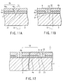
FIG. 5 is a cross-sectional view schematically
showing the photovoltaic module according to the third
embodiment of the present invention. The module 1
shown in FIG. 5 is constructed in almost the same
manner as the module 1 shown in FIG. 4 except that
a fourth separation groove 25 is disposed therein.
The fourth separation groove 25 is provided such
that the third separation groove 24 is interposed
between the first separation groove 21 and the fourth
separation groove 25, and has an opening at a level of
an interface between the front electrode 3 and the
photovoltaic layer 4a and a bottom surface constituted
by the surface of the substrate 2. This fourth
separation groove 25 is filled, in the same manner as
the first separation groove 21, with the amorphous
material constituting the photovoltaic layer 4a.
According to this structure, even if a conductive
path is formed so as to extend from the interlayer 23
disposed close to the cell to the front electrode 3,
there is little possibility that an electric conductive
path can be formed starting from the interlayer 5 of
one of adjacent cells 10 and reaching the front
electrode 3 of the other of the cells 10 due to the
provision of the separation groove 25 between the
separation groove 24 and the connection groove 23.
Therefore, according to the module 1 shown in FIG. 5,
the generation of side leak due to the formation of
conductive path can be prevented, thereby making it
possible to realize higher output performance.
Further, since the formation of the separation
groove 24 can be performed concurrent with the
formation of the separation groove 21, the number of
steps is not required to be increased. Namely,
according to the third embodiment, almost the same
effects as obtainable in the second embodiment can
be obtained, and at the same time, higher output
performance can be easily realized without increasing
the number of steps.
In this third embodiment, the specific resistance
and thickness of the interlayer 5 should preferably be
selected from those described with reference to the
first embodiment. Namely, the specific resistance of
the interlayer 5 should preferably be confined within
the range of 1.0 × 10⁻³Ω·cm to 1.0 × 10⁻¹Ω·cm,
preferably within the range of 1.0 × 10⁻³Ω·cm to 1 ×
10-2Ω·cm. Further, this thickness of the photovoltaic
layers 4a and 4b should preferably be selected also
from those described with reference to the first
embodiment. When the thickness of the photovoltaic
layers 4a and 4b is confined as mentioned above,
it becomes possible to easily well-balance the output
current of the photovoltaic layer 4a with the output
current of the photovoltaic layer 4b, while making it
possible to further enhance the effect of suppressing
the generation of leak current.
Next, a fourth embodiment of the present invention
will be explained. According to the aforementioned
third embodiment, although the generation of side leak
can be prevented more effectively without increasing
the number of steps, the number of grooves to be formed
will be increased by the provision of the separation
groove 25 as compared with the second embodiment.
Whereas, according to the fourth embodiment to be
explained below, the generation of side leak can be
prevented without increasing the number of grooves
which are required to be formed.
FIG. 6 is a cross-sectional view schematically
showing the photovoltaic module according to the fourth
embodiment of the present invention. The module 1
shown in FIG. 6 is constructed in almost the same
manner as the module 1 shown in FIG. 4 except that the
third separation groove 24 is disposed so as to divide
not only the photovoltaic layer 4a and the interlayer 5
but also the transparent front electrode 3.
According to this structure, since a pair of front
electrodes 3 which are placed on both sides of the
separation groove 24 are electrically insulated, even
if the sidewall of the separation groove 24 is adhered
with conductive fine particles, there is little
possibility that an electric conductive path can be
formed starting from the interlayer 5 of one of
adjacent cells 10 and reaching the front electrode 3
of the other of the cells 10. Therefore, according to
the module 1 shown in FIG. 6, the generation of side
leak via the interior of groove can be prevented,
thereby making it possible to realize higher output
performance. Namely, according to the fourth
embodiment, the aforementioned generation of side leak
can be prevented without increasing the number of
grooves which are required to be formed.
According to this fourth embodiment, since the
separation groove 24 is provided as in the second
embodiment, it is possible to prevent the generation
of leak current between the region of the interlayer
5 which is located inside the cell 10 and the metal
filling the connection groove 23.
Further, according to this fourth embodiment,
since the separation groove 24 is provided independent
from the separation groove 21 as in the second
embodiment, the generation of electric short-circuit
between the front electrodes 3 of adjacent cells 10 can
be effectively prevented.
By the way, according to the structure shown in
FIG. 6, since the bottom surface of the separation
groove 24 is constituted by the surface of the
substrate 2, a thin amorphous layer may be caused to
grow inside the separation groove 24 at the initial
stage in the process of forming the photovoltaic layer
104b. In this case, as explained above, part of the
photovoltaic layer 4b may be caused to peel away from
the separation groove 24. If such a peeling is caused
to occur in the module 101 shown in FIG. 3A, the
separation groove 121 may be filled with a conductive
material such as metal on the occasion of forming the
back electrode 106, thereby permitting the generation
of short-circuit between the back electrode 106 and the
front electrode 103 inside a single cell 110, resulting
in a prominent deterioration of output performance.
Whereas, according to the module 1 shown in FIG. 6,
since the separation groove 24 is disposed independent
from the separation groove 21, even if such a peeling
is caused to occur, there is little possibility that
the output performance will be badly deteriorated.
Namely, according to the fourth embodiment, it is
possible to easily realize high output performance as
in the case of the third embodiment.
In this fourth embodiment, the specific resistance
and thickness of the interlayer 5 should preferably be
selected from those described with reference to the
first embodiment. Namely, the specific resistance of
the interlayer 5 should preferably be confined within
the range of 1.0 × 10⁻³Ω·cm to 1.0 × 10⁻¹Ω·cm,
preferably within the range of 1.0 × 10⁻³Ω·cm to 1 ×
10-2Ω·cm. Further, this thickness of the photovoltaic
layers 4a and 4b should preferably be selected also
from those described with reference to the first
embodiment. When the thickness of the photovoltaic
layers 4a and 4b is confined as mentioned above, it
becomes possible to easily well-balance the output
current of the photovoltaic layer 4a with the output
current of the photovoltaic layer 4b, while making it
possible to further enhance the effect of suppressing
the generation of leak current.
Next, a fifth embodiment of the present invention
will be explained.
The present inventors have investigated as for the
reasons which make it difficult to realize high output
performance when the structure shown in FIGS. 3A and 3B
is applied to the hybrid-type module. Namely, the
present inventors have investigated with regard to
the reasons why the effects to be obtained when the
aforementioned separation groove is formed in the
interlayer differ greatly between the tandem-type
structure where each of the photovoltaic layers
comprises an amorphous semiconductor layer and the
hybrid-type structure. As a result, the following fact
is found to be also one of the main reasons.
Generally, the separation groove for preventing
side leak is disposed so as to divide not only the
interlayer but also the photovoltaic layer interposed
between the interlayer and the front electrode.
The reason for this is that the dividing of the
interlayer is performed by an indirect method wherein
the underlying photovoltaic layer is irradiated with
a laser beam from the glass substrate side so as to
fuse or sublimate the photovoltaic layer, thereby
converting the light energy into the heat and/or
kinetic energy, which is then employed for removing
the regions corresponding to the laser beam-irradiated
portions of the interlayer.
When the separation groove is formed in this
manner, conductive fine particles are caused to be
produced simultaneous with the dividing of the
interlayer and are then permitted to adhere onto
the sidewall and bottom of the separation groove.
Since the conductive fine particles being adhered onto
the sidewall and bottom of the separation groove are
generally distributed at a relatively low density, the
conductive fine particles can be electrically insulated
from each other as long as the conductivity of the
material filling the separation groove is sufficiently
low. Namely, there is little possibility that the
conductive fine particles that have been adhered
onto the sidewall and bottom of the separation groove
will form a conductive path. For this reason, the
generation of side leak can be prevented in the tandem-type
structure wherein the separation groove is filled
with an amorphous material which is relatively low in
conductivity.
Whereas, in the hybrid-type structure, since
the separation groove is filled with a crystalline
substance which is relatively high in conductivity,
the insulation between conductive fine particles
that have been adhered onto the sidewall and bottom
of the separation groove would become insufficient.
Therefore, in the hybrid-type structure, a conductive
path extending from the interlayer via the sidewall,
etc. of the separation groove to the front electrode
will be formed, thereby permitting side leak to be
generated. This is a third reason.
Based on the aforementioned findings, the present
inventors have repeated an intensive study with an
assumption that the side leak can be prevented if the
conductive fine particles that have been adhered onto
the sidewall and bottom of the separation groove can
be removed. As a result, it has been found that when
an etching method is utilized for the removal of
the conductive fine particles, the conductive fine
particles can be easily and reliably removed from
the sidewall and bottom of the separation groove, and
at the same time, the surface of the interlayer can
be roughened, thereby forming a surface-textured
structure, and enabling to easily realize high output
performance.
FIG. 7 is a cross-sectional view schematically
showing the photovoltaic module according to a fifth
embodiment of the present invention. The module 1
shown in FIG. 7 is constructed in almost the same
manner as the module 1 shown in FIG. 4 except that
the interlayer 5 is provided with a surface-textured
structure.
As shown in FIG. 7, although the third separation
groove 24 is interposed between the first separation
groove 21 and the connection groove 23, this third
separation groove 24 may be disposed in a manner that
the first separation groove 21 is interposed between
the third separation groove 24 and the connection
groove 23. However, when the third separation groove
24 is interposed between the first separation groove 21
and the connection groove 23 as shown in FIG. 7, the
effective area useful for the generation of power can
be easily enlarged.
The aforementioned module 1 according to this
embodiment can be manufactured by the method explained
as follows.
First of all, a transparent front electrode 3 is
formed as a continuous film on one of main surfaces
of the transparent substrate 2. Then, the first
separation groove 21 is formed in the front electrode 3
by means of a laser-scribing using YAG laser to divide
the front electrode 3 correspondently with each of the
cells 10.
Then, the photovoltaic layer 4a is formed as a
continuous film on the front electrode 3. As a result
of the formation of the photovoltaic layer 4a, the
first separation groove 21 that has been formed in the
front electrode 3 is concurrently filled with the
amorphous material constituting the photovoltaic layer
4a. Then, the interlayer 5 is formed as a continuous
film on the photovoltaic layer 4a. Thereafter, by
means of a laser-scribing using YAG laser, the
third separation groove 24 is formed to divide
the photovoltaic layer 4a and the interlayer 5.
These steps are the same as explained in the second
embodiment.
Further, due to the a laser-scribing of the
photovoltaic layer 4a and the interlayer 5, conductive
fine particles are permitted to adhere onto the
sidewall and bottom of the third separation groove 24.
These conductive fine particles are subsequently
removed by means of etching method in this embodiment.
FIGS. 8A and 8B are cross-sectional views
schematically showing the third separation groove 24
and the interlayer 5 before and after the etching
treatment, respectively. As shown in FIG. 8A, at the
moment immediately after the formation of the third
separation groove 24, the conductive fine particles 30
are adhered onto the sidewall and bottom of the third
separation groove 24. If the second photovoltaic layer
4b is formed under this condition, the third separation
groove 24 will be filled with a crystalline material,
and hence the insulation between the conductive fine
particles 30 would become incomplete. As a result,
a conductive path extending from the interlayer or the
p-type or the intrinsic semiconductor layer of the
second photovoltaic layer 4b of the left side via the
left side sidewall of the third separation groove 24 to
the right side transparent electrode 3 (as viewed in
these drawings) will be formed. If so, it would be
impossible of course to effectively take up the
electric power that has been generated in the second
photovoltaic layer 4b.
Whereas, in this embodiment, since the surface of
the structure in which the interlayer 5 is provided is
subjected to etching prior to the formation of the
second photovoltaic layer 4b, the conductive fine
particles 30 can be removed from the sidewall and
bottom of the third separation groove 24 as shown in
FIG. 8B. As a result, it is now possible according
to this embodiment to prevent the formation of the
aforementioned conductive path and to effectively take
up the electric power that has been generated in the
second photovoltaic layer 4b.
Further, if the etching is performed in this
manner, the surface of the interlayer 5 would be
roughened to form so-called "surface-textured
structure" or a "textured pattern" on the surface of
the interlayer 5. This surface-textured structure
is capable of providing the interface between the
interlayer 5 and the photovoltaic layer 4b with a large
number of arrayed reflective surfaces each inclined
at an acute angle with respect to the surface of
substrate, thereby enabling the light that has been
entered into the photovoltaic layer 4b to be
effectively confined therein. Therefore, it is
possible, according to this embodiment, to improve the
output performance of the second photovoltaic layer 4b.
It would be preferable to employ an etching
solution having a pH ranging from 4 to 10 in the
aforementioned etching process. Because if the pH is
less than 4 or higher than 10, the etching rate of the
interlayer 5 would become excessively high, thereby
making it difficult to control the thickness of the
interlayer 5.
As for the etching solution, it is possible to
employ an acid such as hydrochloric acid, nitric acid
and sulfuric acid; or an alkali such as an NaOH
solution. It is also possible to employ water in this
case, because water is capable of dissolving therein
carbon dioxide in air atmosphere to thereby form
carbonic acid.
Preferably, the etching treatment to the surface
of the structure in which the interlayer 5 is provided
should be performed using the aforementioned etching
solution while applying thereto an ultrasonic
vibration. If the etching is performed in this manner,
the removal of the conductive fine particles 30 and
the formation of the surface-textured structure can be
accomplished within an etching time of several to
several tens seconds in general.
Upon finishing the aforementioned etching
treatment, the surface having the interlayer 5 is
allowed to dry, and the photovoltaic layer 4b is
deposited as a continuous film on the surface of the
interlayer 5. As a result of the deposition of this
photovoltaic layer 4b, the third separation groove 24
is concurrently filled with the crystalline material
constituting this photovoltaic layer 4b.
Subsequently, the connection groove 23 passing
through the photovoltaic layers 4a and 4b and through
the interlayer 5 is formed by means of a laser-scribing
using YAG laser, etc. Then, the back electrode 6 is
formed on the photovoltaic layer 4b. As a result of
the formation of this back electrode 6, the connection
groove 23 is concurrently filled with a conductive
material, thereby permitting the back electrode 6 to be
electrically connected with the front electrode 3 via
the conductive material filling the connection groove
23. Then, the second separation groove 22 is formed in
the photovoltaic layers 4a and 4b, the interlayer 5,
and the back electrode 6 by means of a laser-scribing
using YAG laser, etc.
Upon finishing the formation of this second
separation groove 22, an etching treatment similar to
that applied to the third separation groove 24 should
preferably be applied to the structure obtained. When
this second separation groove 22 is formed as described
above, conductive fine particles are permitted to
adhere onto the inner wall as well as onto the bottom
surface of this second separation groove 22 in the
same manner as explained with reference to the third
separation groove 24. However, by contrast to the
third separation groove 24, there is little possibility
that the second separation groove 22 is filled with
a highly conductive material, thereby making it
relatively difficult to allow the side leak originating
from the conductive fine particles to take place.
However, when the aforementioned etching is performed
upon finishing the formation of this second separation
groove 22, it would become possible to reliably realize
sufficiently high output performance.
Upon finishing the aforementioned etching
treatment, the resultant surface is allowed to dry.
Then, a power-generating region is delimited by means
of a laser-scribing using YAG laser, etc. Further, a
pair of bus bar electrodes 12 are attached to the both
sides of the array constituted by the cells 10, thus
obtaining the structure as shown in FIG. 7.
As explained above, according to the method of
this embodiment, it is possible, by way of very simple
etching process, to easily and reliably remove the
conductive fine particles 30 from the sidewall and
bottom of the separation groove 24, and at the same
time, to roughen the surface of the interlayer 5 so as
to obtain a surface-textured structure. Therefore,
according to this embodiment, it is possible to easily
realize high output performance of module.
Next, a sixth embodiment of the present invention
will be explained.
The present inventors have investigated as for the
reasons which make it difficult to realize high output
performance when the structures shown in FIGS. 3A and
3B are applied to the hybrid-type module. Namely, the
present inventors have investigated with regard to the
reasons why the effects to be obtained when the
aforementioned separation groove is formed in the
interlayer differ greatly between the tandem-type
structure where each of the photovoltaic layers
includes an amorphous semiconductor layer and the
hybrid-type structure. As a result, the following
fact is found to be also one of the main reasons.
Generally, in the manufacture of tandem-type
photovoltaic module, laser is employed for forming
the connection groove thereof. For instance, on the
occasion of forming the connection groove, a laser beam
is scanned from the substrate side onto a laminate
structure of the first photovoltaic layer, an
interlayer and a second photovoltaic layer which is
formed on the surface of transparent substrate where
the front electrode thereof is formed in advance.
In this case, the laser beam can be hardly absorbed by
the front electrode and the interlayer, but can be
mainly absorbed by the first and second photovoltaic
layers. As a result, the first and second photovoltaic
layers will be selectively fused or sublimed at the
laser beam-irradiated portion thereof. Further, the
portion of the interlayer which corresponds to the
laser beam-irradiated portion is eliminated due to
the heat and/or kinetic energy generated as a result
of the fusion or sublimation of the underlying first
photovoltaic layer. In this manner, the connection
groove dividing the laminate structure of the first
photovoltaic layer, the interlayer and the second
photovoltaic layer will be formed.
It is important in this method to enable both of
the first and second photovoltaic layers to be suitably
fused or sublimed. In the ordinary tandem-type
structure, an amorphous semiconductor layer which is
capable of exhibiting a high light-absorption
coefficient to the laser beam such as an amorphous
silicon layer is employed, so that the connection
groove could be formed using a relatively low laser
power.
However, a crystalline semiconductor layer such
as a crystalline silicon layer is very low in light-absorption
coefficient as compared with an amorphous
semiconductor layer such as an amorphous silicon layer.
Therefore, it is difficult, in the manufacture of the
hybrid-type photovoltaic module, to sufficiently fuse
or sublime the second photovoltaic layer by making use
of the aforementioned low laser power. Therefore, it
is required to enhance the laser power. However, if
the laser power is enhanced, the front electrode, etc.
would be damaged. This is the fourth reason.
By taking the aforementioned factors into
consideration, the present inventors have made an
intensive study with respect to the structure of the
hybrid-type photovoltaic module. As a result, the
present inventors has found that, when the separation
groove dividing the front electrode and the separation
groove disposed for preventing the side leak and
dividing both of the first photovoltaic layer and the
interlayer are joined to form the first separation
groove, the ratio of the amorphous phase occupying the
interior of the first separation groove is very high in
spite of the fact that the semiconductor layer in the
second photovoltaic layer is crystalline. It is also
found out that this amorphous phase is not confined to
the interior of the first separation groove but is
spread out to an upper portion of the first separation
groove of the second photovoltaic layer as well as up
to a peripheral region thereof.
Further, the present inventors have noticed
that according to the prior art, the first separation
groove is spaced apart from the connection groove.
As a result, present inventors has found that, if the
connection groove is formed in such a way that the
connection groove borders on the first separation
groove, the irradiation of laser beam for forming the
connection groove can be performed against the portion
of the second photovoltaic layer where the ratio of
amorphous phase is high, thereby enabling the second
photovoltaic layer to be sufficiently fused or sublimed
using such a relatively low laser power that would not
give any substantial damage to the front electrode,
etc., and additionally enabling the area of module
useful for the power generation to be further
increased.
FIG. 9 a cross-sectional view schematically
showing the photovoltaic module according to a sixth
embodiment of the present invention. The module 1
shown in FIG. 9 is constructed in almost the same
manner as the module 1 shown in FIG. 4 except that the
first separation groove 21 divides not only the front
electrode 3 but also the first photovoltaic layer 4a
and the interlayer 5. Namely, in the module 1 shown in
FIG. 9, the first separation groove 21 thereof
functions not only as the first separation groove 21
but also as the third separation groove 23 of the
module 1 shown in FIG. 4. Further, according to the
module 1 shown in FIG. 9, the connection groove 23
borders on the first separation groove 21 and also
on the second separation groove 22. Although the
connection groove 23 borders on the second separation
groove 22 in the embodiment shown in FIG. 9, these
grooves may be spaced apart from each other.
The module 1 according to this embodiment can be
manufactured by the method as explained below with
reference to FIGS. 10A to 10G. Namely, FIGS. 10A to
10G are cross-sectional views schematically showing
the method of manufacturing the photovoltaic module
according to a sixth embodiment of the present
invention.
For the manufacture of the module 1 shown in
FIG. 10G, at first, prepared is a transparent substrate
2 on one main surface of which is provided with a
transparent front electrode 3 in a form of a continuous
film as shown in FIG. 10A. Then, as shown in FIG. 10B,
a photovoltaic layer 4a and an interlayer are
successively deposited as a continuous film
respectively on the surface of the front electrode 3.
Then, as shown in FIG. 10C, a first laminate
structure including the front electrode 3, the
photovoltaic layer 4a and the interlayer 5 is divided
by means of a laser-scribing using YAG laser, etc.
As a result, the first laminate structure divided by
the first separation groove 21 will be obtained.
By the way, the electrically conductive fine particles
to be produced as a result of the laser-scribing of the
interlayer 5 are removed as required by means of
ultrasonic cleaning, etc.
Then, as shown in FIG. 10D, the photovoltaic layer
4b is formed as a continuous film on the interlayer 5.
As a result of the formation of the photovoltaic layer
4b, the first separation groove 21 is concurrently
filled with the material constituting the photovoltaic
layer 4b.
Generally, since the interlayer 5 is formed of
a crystalline material, the semiconductor layer of
photovoltaic layer 4b to be deposited on the interlayer
5 can be made crystalline. However, because of the
reason that the transparent substrate 21 is amorphous,
it would be generally difficult to enable a crystal
growth to take place inside the first separation groove
21. Therefore, the ratio of amorphous phase in the
material filling the first separation groove 21 would
be naturally increased, and at the same time, the ratio
of amorphous phase at and near the region over the
separation groove 21 of the photovoltaic layer 4b would
be increased. Accordingly, the photovoltaic layer 4b
would be constituted by an amorphous portion 4b1 which
contains a relatively high ratio of amorphous phase,
and by a crystalline portion 4b2 which is formed
substantially only of crystalline phase.
By the way, a portion of the photovoltaic layer 4b
which is disposed at the regions inside and periphery
of the separation groove 21 is caused to peel off along
with the photovoltaic layer 4a and the interlayer 5
during the process of forming the photovoltaic layer 4b
or during the post process thereof. The peeling of
this kind can be prevented by suitably adjusting the
deposition conditions.
Thereafter, as shown in FIG. 10E, by means of
a laser-scribing using YAG laser, etc., the connection
groove 23 is formed in a second laminate structure
including the photovoltaic layer 4a, the interlayer 5
and the photovoltaic layer 4b. According to this
embodiment, since the connection groove 23 borders
on the first separation groove 21, the laser beam
irradiation for forming the connection groove 23 can
be selectively applied to the amorphous portion 4b1
exhibiting a far higher light-absorption coefficient as
compared with the crystalline portion 4b2. Therefore,
the connection groove 23 can be formed using such a low
laser power that would not give any substantial damage
to the transparent front electrode 3, etc.
Then, as shown in FIG. 10F, a back electrode 6 is
formed on the photovoltaic layer 4b. As a result of
the formation of this back electrode 6, the connection
groove 23 is concurrently filled with a conductive
material such as metal, thereby electrically connecting
the back electrode 6 with the front electrode 3 via the
conductive material filling the connection groove 23.
Then, as shown in FIG. 10G, by means of a laser-scribing
using YAG laser, etc., the second separation
groove 22 is formed in a third laminate structure
including the photovoltaic layer 4a, the interlayer 5,
the photovoltaic layer 4b and the back electrode 6.
Then, a power-generating region is delimited by means
of a laser-scribing using YAG laser, etc. Further, a
pair of bus bar electrodes 12 are attached to the both
sides of the array constituted by the cells 10, thus
obtaining the structure as shown in FIGS. 9 and 10G.
As explained above, in the module according to
this embodiment, the interlayer 5 is electrically
insulated from the conductive material filling the
connection groove 23 by the separation groove 21.
Therefore, the generation of leak current between
these regions can be prevented. According to this
embodiment, since the connection groove 23 borders
on the first separation groove 21, the laser beam
irradiation for forming the connection groove 23 can
be selectively applied to the amorphous portion 4b1
exhibiting a far higher photo-absorption coefficient as
compared with the crystalline portion 4b2. Therefore,
the connection groove 23 can be formed using such a low
laser power that would not give any substantial damage
to the transparent front electrode 3, etc. Further,
according to this embodiment, since the connection
groove 23 borders on the first separation groove 21,
the area of module useful for the power generation can
be further increased.
According to the embodiment described above, the
dividing of the front electrode 3 and the dividing of
the photovoltaic layer 4a and the interlayer 5 are
concurrently performed in the same single step.
However, these division may be performed separately.
Further, according to the embodiment described above,
the connection groove 23 borders on the second
separation groove 22. However, these grooves may be
spaced apart from each other. However, when the
connection groove 23 borders on the second separation
groove 22, the area useful for the power generation can
be increased, thereby making it advantageous in this
respect.
Preferably, the formation of the second separation
groove 22 and the connection groove 23 should be
performed by the method shown in FIGS. 11A and 11B.
FIG. 11A is a cross-sectional view schematically
showing one example of the forming method of the
connection groove 23 of the photovoltaic module 1 shown
in FIGS. 9 and 10G. FIG. 11B is a cross-sectional view
schematically showing one example of the method of
forming a second separation groove 22 of the photovoltaic
module 1 shown in FIGS. 9 and 10G. FIG. 12 is
a cross-sectional view schematically showing the
photovoltaic module to be obtained by the method
illustrated in FIGS. 11A and 11B. The reference
numeral 33 in FIG. 11A represents a region where the
connection groove 23 is to be formed, while the
reference numeral 32 in FIG. 11B represents a region
where the second separation groove 22 is to be formed.
The connection groove 23 may be formed in such
a manner that as shown in FIG. 11A, the scanning of
laser beam 31 is performed so as to enable the beam
spot of laser beam 31 to lie across one of the
sidewalls of the first separation groove 21. If the
scanning of laser beam is performed in this manner,
even if the relative position of the center of laser
beam 31 to the first separation groove 21 is caused to
fluctuate more or less in the lateral direction in the
drawing, the connection groove 23 can be reliably
formed without leaving a residual matter at a region
between the first separation groove 21 and the
connection groove 23. By the way, when the connection
groove 23 is formed in this manner, the first
separation groove 21 is caused to overlap with the
connection groove 23 as shown in FIG. 11B. Therefore,
the module to be obtained in this manner would be
constructed such that a portion of the bottom of the
connection groove 23 is constituted by the surface of
the transparent substrate 2 while the rest of the
bottom of the connection groove 23 is constituted by
the surface of the front electrode 3 as shown in
FIG. 12.
Similarly, the second separation groove 22 may be
formed in such a manner that as shown in FIG. 11B, the
scanning of laser beam 31 is performed so as to enable
the beam spot of laser beam 31 to lie across one of
the sidewalls of the connection groove 23 (i.e. the
sidewall located remote from the first separation
groove 21). If the scanning of laser beam is performed
in this manner, even if the relative position of the
center of laser beam 31 to the connection groove 23
is caused to fluctuate more or less in the lateral
direction in the drawing, the second separation groove
22 can be reliably formed without leaving a residual
matter at a region between the second separation groove
22 and the connection groove 23. Furthermore, when the
second separation groove 22 is formed in this manner,
the second separation groove 22 is disposed bordering
on the connection groove 23 as shown in FIG. 12, so
that the area which is useful for the generation of
electric power can be advantageously increased.
By the way, as for the laser to be employed for
forming the separation groove or the connection groove,
a pulse laser is generally employed, so that the
adjustment of the power of the laser beam 31 can be
performed by changing the cycle of pulse. Therefore,
when the second separation groove 22 is to be formed,
a portion of the beam spot is required to be partially
superimposed on the position of the beam spot of one
cycle before.
However, when the power of laser beam 31 is
lowered in order to prevent the front electrode 3 from
being damaged on the occasion of forming the second
separation groove 22, the cycle of pulse would be
enlarged, and hence, merely an array of plural number
of holes would be formed without forming the second
separation groove 22 in an extreme case. Further,
even if it is possible to form the second separation
groove 22, it may become difficult to realize such a
sufficient insulating/separating property as expected.
Whereas, when the scanning of laser beam 31 is
performed as shown in FIG. 11B on the occasion of
forming the second separation groove 22, part of the
laser beam 31 would be used to irradiate the metallic
material filling the connection groove 23. The
metallic material filled in the connection groove 23
reflects part of the laser beam 31 and also mediates
the heat conduction between the photovoltaic layers
4a and 4b, as well as the heat conduction between any
of the photovoltaic layers 4a and 4b and the back
electrode 6. Accordingly, even if the power of the
laser beam 31 is high, it is possible to realize a
uniform heating while preventing the front electrode,
etc. from being damaged. Namely, the second separation
groove 22 which is excellent in insulating/isolating
property can be reliably formed.
In this sixth embodiment, the specific resistance
and thickness of the interlayer 5 should preferably be
selected from those described with reference to the
first embodiment. Namely, the specific resistance of
the interlayer 5 should preferably be confined within
the range of 1.0 × 10⁻³Ω·cm to 1.0 × 10⁻¹Ω·cm,
preferably within the range of 1.0 × 10⁻³Ω·cm to 1 ×
10-2Ω·cm. Further, this thickness of the photovoltaic
layers 4a and 4b should preferably be selected also
from those described with reference to the first
embodiment. When the thickness of the photovoltaic
layers 4a and 4b is confined as mentioned above, it
becomes possible to easily well-balance the output
current of the photovoltaic layer 4a with the output
current of the photovoltaic layer 4b, while making it
possible to further enhance the effect of suppressing
the generation of leak current.
The techniques illustrated in the aforementioned
first through sixth embodiments may be optionally
combined. For example, the technique of the first
embodiment may be combined with any of the techniques
of the aforementioned second to sixth embodiments.
Further, the technique of the fifth embodiment may be
combined with any of the techniques of the aforementioned
second to fourth embodiments and sixth
embodiment.
Next, specific examples of the present invention
will be explained.
(Example 1)
By the following method, the photovoltaic module 1
shown in FIGS. 1 and 2 was manufactured.
First of all, a glass substrate of 100 mm × 30 mm
in size whose main surface is provided with an SnO2
film 3 was prepared. Then, with use of YAG pulse
laser, a laser-scribing of the SnO2 film 3 was
performed by laser-scanning parallel with one edge of
the substrate 2, thereby forming separation grooves
21 which divide the SnO2 film 3 into a plurality of
stripe-like patterns. Then, by means of plasma CVD
method, a photovoltaic layer 4a having a thickness
of 0.2 µm was deposited on the SnO2 film 3. This
photovoltaic layer 4a had a p-i-n junction, and a
non-doped amorphous silicon layer was included therein
as a semiconductor layer.
Then, a ZnO layer 5 having a thickness of 50 nm
and containing Al at a concentration of 2% was
deposited on the surface of the photovoltaic layer
4a by means of sputtering method under the conditions
of: 150°C in temperature, 0.53 Pa (4 mTorr) in
pressure, and 20 sccm in Ar flow rate. By the way, in
this example, the ZnO layer 5 was further doped with
0.1% in concentration of Ga in addition to Al. The
specific resistance of this ZnO layer 5 thus formed
was 3 × 10⁻²Ω·cm.
Subsequently, by means of plasma CVD method,
a photovoltaic layer 4b having a thickness of 3.0 µm
was formed on the surface of the ZnO layer 5.
This photovoltaic layer 4b included a non-doped
polycrystalline silicon layer as an intrinsic
semiconductor layer.
Then, with use of YAG SHG pulse laser, a laser-scribing
of a laminate structure including the
photovoltaic layers 4a, 4b and the ZnO layer 5 was
performed by laser-scanning parallel with one edge of
the substrate 2, thereby forming connection grooves 23
dividing this laminate structure into a plurality of
stripe-like patterns.
Thereafter, by means of sputtering method, a ZnO
film and an Ag film were successively deposited on the
surface of the photovoltaic layer 4b to form a back
electrode 6. Then, with use of YAG SHG pulse laser,
a laser-scribing of a laminate structure including
the photovoltaic layers 4a and 4b, the ZnO layer 5 and
the back electrode 6 was performed by laser-scanning
parallel with one edge of the substrate 2, thereby
forming a separation groove 22 dividing the laminate
structure into a plurality of stripe-like patterns.
Then, a laser scanning along the periphery of the
substrate 2 was performed with use of YAG pulse laser,
thereby forming a groove in a laminate structure of the
SnO2 film 3, the photovoltaic layers 4a and 4b, the ZnO
layer 5 and the back electrode 6, so as to delimit the
power generation region. As a result, ten columns of
photovoltaic cells 10 each having a width of about
10 mm and length of about 30 mm and connected in series
with each other were formed. Further, a pair of bus
bar electrodes 12 were attached to both ends of series
array 11 constituted by the cells 10, thereby obtaining
the module 1 as shown in FIGS. 1 and 2.
Then, the output performance of this module 1 was
investigated at a measuring temperature of 25°C by
utilizing a solar simulator in which an irradiance
was set at 100 mW/cm2 and a spectrum was set at AM 1.5.
By the way, as for the light source, a combination of
a xenon lamp, a halogen lamp and a filter was employed.
As a result, an open-circuit voltage of 1.310V,
a short-circuit current density of 12.4 mA/cm2, a fill
factor of 68.4%, and a power generation efficiency of
11.1% were obtained in each cell 10 of this module 1.
(Example 2)
A photovoltaic module 1 as shown in FIGS. 1 and 2
was manufactured in the same manner as explained in
Example 1 except that oxygen was added into the Ar gas
flow at a concentration of several % on the occasion of
forming the ZnO film 5 and the ZnO film 5 was not doped
with Ga. The module 1 thus obtained was featured in
that the ZnO film 5 thereof contained a higher
concentration of oxygen as compared with the module 1
of Example 1. Further, according to the module 1 of
this example, the ZnO film 5 contained Al at a
concentration of 2%, and the specific resistance
thereof was 1 × 10⁻³Ω·cm.
Then, the output performance of this module 1 was
investigated under the same conditions as explained in
Example 1. As a result, an open-circuit voltage of
1.290V, a short-circuit current per unit area of
12.1 mA/cm2, a fill factor of 64.9%, and a power
generation efficiency of 10.1% were obtained in each
cell 10 of this module 1.
(Example 3)
A photovoltaic module 1 as shown in FIGS. 1 and 2
was manufactured in the same manner as explained in
Example 1 except that oxygen was added into the Ar gas
flow at a concentration of several % on the occasion of
forming the ZnO film 5. The module 1 thus obtained was
featured in that the ZnO film 5 thereof contained a
higher concentration of oxygen as compared with the
module 1 of Example 1. Further, according to the
module 1 of this example, the ZnO film 5 contained
Al at a concentration of 2% and Ga at a concentration
of 0.1% and the specific resistance thereof was
9 × 10⁻²Ω·cm.
Then, the output performance of this module 1 was
investigated under the same conditions as explained in
Example 1. As a result, an open-circuit voltage of
1.320V, a short-circuit current per unit area of
12.5 mA/cm2, a fill factor of 66.3%, and a power
generation efficiency of 10.9% were obtained in each
cell 10 of this module 1.
(Comparative Example 1)
A photovoltaic module 1 as shown in FIGS. 1 and 2
was manufactured in the same manner as explained in
Example 1 except that the ZnO film 5 was not doped with
Ga. The concentration of oxygen in the ZnO film 5 of
this module 1 was almost the same as that of the module
1 of Example 1. Further, according to the module 1 of
this comparative example, the ZnO film 5 contained Al
at a concentration of 2%, and the specific resistance
thereof was found 4 × 10⁻⁴Ω·cm.
The specific resistance of the
ZnO film 5 of
the
module 1 according to Examples 1 to 3 and to
Comparative Example 1, as well as the output
performance of the
module 1 are summarized in the
following Table 1.
| | Specific resistance (Ω·cm) | Output performance |
| | | VOC (V) | JSC (mA/cm2) | F.F. (%) | Eff. (%) |
| Example 1 | 3 × 10⁻² | 1.310 | 12.4 | 68.4 | 11.1 |
| Example 2 | 1 × 10⁻³ | 1.290 | 12.1 | 64.9 | 10.1 |
| Example 3 | 9 × 10⁻² | 1.320 | 12.5 | 66.3 | 10.9 |
| Comparative example 1 | 4 × 10⁻⁴ | 1.260 | 12.1 | 60.8 | 9.3 |
In the above Table 1, "VOC" denotes the open-circuit
voltage, and "JSC" a short-circuit current per
unit area. Further, "F.F." denotes a fill factor, and
"Eff" a conversion efficiency.
As apparent from Table 1, when the specific
resistance of ZnO film 5 was equal to or higher than
1 × 10⁻³Ω·cm, it was possible to realize a higher
power generation efficiency. Further, when the
specific resistance of ZnO film 5 was equal to or
higher than 1 × 10⁻²Ω·cm, it was possible to realize
a much higher conversion efficiency.
It would be clear through the comparison of
Examples 1 and 2 with Comparative Example 1 that as
the specific resistance of ZnO film 5 was increased,
the conversion efficiency was proportionally improved.
Whereas, it is clear from the comparison between
Example 1 and Example 3 that as the specific resistance
of ZnO film 5 was increased, the conversion efficiency
was proportionally deteriorated. These results
indicate that the generation of leak current can be
suppressed by increasing the specific resistance of
ZnO film 5, and that if the specific resistance of
ZnO film 5 becomes excessively high, the electric
connection between photovoltaic layers 4a and 4b would
be obstructed. By the way, as long as the specific
resistance of ZnO film 5 is equal to or lower than 1 ×
10-1Ω·cm, it was possible to prevent the electric
connection between photovoltaic layers 4a and 4b from
being badly obstructed.
Next, a plurality of photovoltaic modules 1
differing in the thickness of ZnO film 5 from each
other were manufactured in the same manner as explained
in Example 1 except that the thickness of ZnO film 5
was altered. Further, a plurality of photovoltaic
modules 1 differing in the thickness of ZnO film 5 from
each other were manufactured in the same manner as
explained in Example 2 except that the thickness of
ZnO film 5 was altered. Additionally, a plurality of
photovoltaic modules 1 differing in the thickness of
ZnO film 5 from each other were manufactured in the
same manner as explained in Example 3 except that
the thickness of ZnO film 5 was altered. Furthermore,
a plurality of photovoltaic modules 1 differing in
the thickness of ZnO film 5 from each other were
manufactured in the same manner as explained in
Comparative Example 1 except that the thickness of
ZnO film 5 was altered.
Then, the relationship between the specific
resistance and the output performance of the ZnO film 5
was investigated on these modules 1. As a result, in
any of these modules, when the thickness of ZnO film 5
was exceeded over 100 nm, the short-circuit current
per unit area was caused to deteriorate badly. It is
assumed that the reason for this attributes to the
fact that when the thickness of ZnO film 5 became
excessively large, the magnitude of light passing
through the ZnO film 5 was caused to decrease, thereby
lowering the output current of the photovoltaic layer
4b. By the way, it was confirmed that when the ZnO
film 5 was formed by the methods of Examples 1 to 3,
the short-circuit current per unit area could be made
sufficiently high as long as the thickness of the ZnO
film 5 was confined to a value equal to or lower than
100 nm, or made much higher as long as the thickness
of the ZnO film 5 was confined to a value equal to or
lower than 70 nm.
On the other hand, when the thickness of the
ZnO film 5 was made less than 5 nm in the modules 1
wherein the ZnO film 5 was deposited by the methods of
Examples 1 to 3, the short-circuit current per unit
area thereof was found slightly higher than the
module 1 of Comparative Example 1, but other output
performance thereof were found almost equivalent to
the module 1 of Comparative Example 1. This can be
attributed to the facts that when the thickness of the
ZnO film 5 is made thinner, the generation of leak
current can be proportionally suppressed, and that if
the thickness of the ZnO film 5 is made excessively
thinner, the magnitude of light to be reflected by the
ZnO film 5 decreases, thereby lowering the output
current of the photovoltaic layer 4a. By the way, when
the ZnO film 5 was deposited to a thickness of 10 nm or
more by the methods of Examples 1 to 3, the output
performance of module could be prominently improved
as compared with the module wherein the ZnO film 5
was formed by the method of Comparative Example 1.
This effect could be made much prominent when the
thickness of ZnO film 5 was increased to 20 nm or more.
(Example 4)
By the following method, the photovoltaic module 1
shown in FIGS. 1 and 4 was manufactured.
First of all, a glass substrate of 127 mm ×
127 mm in size whose main surface was provided with
an SnO2 film 3 was prepared. Then, with use of YAG IR
pulse laser, a laser-scribing of the SnO2 film 3 was
performed by laser-scanning parallel with one edge of
the substrate 2, thereby forming separation grooves 21
each having a width of 40 µm and dividing the SnO2
film 3 into a plurality of stripe-like patterns.
Subsequently, the resultant structure was
subjected to ultrasonic cleaning and drying processes.
Further, by means of plasma CVD method, a photovoltaic
layer 4a was formed on the surface of the SnO2 film 3.
By the way, this photovoltaic layer 4a had a p-i-n
junction, and a non-doped amorphous silicon layer
was included therein as a semiconductor layer. Then,
a ZnO layer 5 was deposited on the surface of the
photovoltaic layer 4a by means of sputtering method.
Then, with use of YAG SHG pulse laser, a laser-scribing
of the photovoltaic layer 4a and the ZnO layer
5 was performed by laser-scanning parallel with one
edge of the substrate 2, thereby forming separation
grooves 24 each having a width of 60 µm and dividing
these layers into a plurality of stripe-like patterns.
By the way, the center-to-center distance between these
separation grooves 21 and 24 was set to 100 µm.
Thereafter, by means of plasma CVD method,
a photovoltaic layer 4b was formed on the ZnO film 5.
By the way, this photovoltaic layer 4b included a non-doped
polycrystalline silicon layer as a semiconductor
layer.
Then, with use of YAG SHG pulse laser, a laser-scribing
of the photovoltaic layers 4a and 4b and the
ZnO layer 5 was performed by laser-scanning parallel
with one edge of the substrate 2. As a result,
connection grooves 23 each having a width of 60 µm and
dividing these layers into a plurality of stripe-like
patterns were formed. By the way, the center-to-center
distance between the connection groove 23 and the
separation groove 24 was set to 100 µm.
Thereafter, by means of sputtering method, a ZnO
film and an Ag film were successively deposited on the
surface of the photovoltaic layer 4b to form a back
electrode 6. Then, by laser-scanning parallel with
one side of the substrate 2 with use of YAG SHG pulse
laser, formed were separation grooves 22 each having
a width of 60 µm and dividing a laminate structure,
which includes the photovoltaic layers 4a and 4b, the
ZnO layer 5 and the back electrode 6, into a plurality
of stripe-like patterns. By the way, the center-to-center
distance between the separation groove 22 and
the connection groove 23 was set to 100 µm.
Then, by laser-scanning along the periphery of the
substrate 2 with use of YAG pulse laser, a groove which
divides a laminate structure including the SnO2 film 3,
the photovoltaic layers 4a and 4b, the ZnO layer 5 and
the back electrode 6 was formed to delimit the power
generation region. As a result, eleven columns of
photovoltaic cells 10 each having a size of 10 mm ×
100 mm and connected in series with each other were
formed.
Further, a pair of bus bar electrodes 12 were
attached to both ends of series array 11 constituted by
the cells 10, thereby obtaining the module 1 as shown
in FIGS. 1 and 4. By the way, plural kinds of modules
1 differing from each other in thickness of the
photovoltaic layers 4a and 4b, and of the ZnO layer
5 were manufactured in this example.
Then, the output performances of these modules 1
manufactured by the aforementioned method were
investigated under the same conditions as explained in
Example 1. The results obtained are shown at the
column of "Example 4" in Table 2.
(Comparative Example 2)
A photovoltaic module having the same structure
as that manufactured in Example 4 except that the
separation groove 24 was not provided therewith was
manufactured. In this comparative example, the
thickness of the
photovoltaic layer 4a was set to
250 nm, the thickness of the
photovoltaic layer 4b was
set to 3000 nm, and the thickness of the
ZnO film 5 was
set to 30 nm. Then, the output performances of these
modules were also investigated. The results obtained
are shown at the column of "Comparative Example 2" in
Table 2.
| | Thickness (nm) | Output performance |
| | Photovoltaic layer | ZnO film | VOC (V) | JSC (mA/cm2) | F.F. (%) | Eff. (%) |
| | 4a | 4b |
| Example 4 | 200 | 3000 | 30 | 1.312 | 12.3 | 64.2 | 10.4 |
| 200 | 3000 | 50 | 1.318 | 12.7 | 65.8 | 11.0 |
| 200 | 3000 | 70 | 1.322 | 12.4 | 67.1 | 11.0 |
| 250 | 2300 | 30 | 1.359 | 12.3 | 63.5 | 10.6 |
| 250 | 2300 | 50 | 1.357 | 11.8 | 64.8 | 10.5 |
| 250 | 2300 | 70 | 1.348 | 11.1 | 66.6 | 10.0 |
| 250 | 3000 | 30 | 1.351 | 12.0 | 63.8 | 10.3 |
| 250 | 3000 | 50 | 1.347 | 12.8 | 64.2 | 11.1 |
| 250 | 3000 | 70 | 1.355 | 12.5 | 65.8 | 11.1 |
| 250 | 3500 | 30 | 1.351 | 12.4 | 64.2 | 10.8 |
| 250 | 3500 | 50 | 1.356 | 13.1 | 63.0 | 11.2 |
| 250 | 3500 | 70 | 1.324 | 12.6 | 65.5 | 10.9 |
| 300 | 3000 | 30 | 1.322 | 13.0 | 65.2 | 11.2 |
| 300 | 3000 | 50 | 1.311 | 12.8 | 66.0 | 11.1 |
| 300 | 3000 | 70 | 1.332 | 12.3 | 65.0 | 10.7 |
| Comparative example 2 | 250 | 3000 | 30 | 1.313 | 12.3 | 50.0 | 8.1 |
As shown in Table 2, all of the modules according
to Example 4 exhibited a far excellent power generation
efficiency as compared with the module according to
Comparative Example 2. This merit may be attributed to
the facts that since the separation groove 24 was
provided in all of the modules according to Example 4,
it was possible to increase the open-circuit voltage
and to greatly increase the fill factor, though the
short-circuit current per unit area was not
substantially changed.
By the way, a photovoltaic module 101 as shown in
FIG. 3A was manufactured almost the same method as
explained in Example 4, and the output performance of
this module 101 were measured. However, when the
output performance of this module 101 were compared
with those of the module 1 according to Example 4,
the output performance of this module 101 were found
insufficient in every respects.
(Example 5)
A photovoltaic module 1 as shown in FIG. 5 was
manufactured in the same manner as explained in
Example 4. Namely, in this example, a separation
groove 25 having a width of 40 µm was also formed in
addition to the separation groove 21 in the step of
forming the separation groove 21. Further, the center-to-center
distance between these separation grooves
21 and 24 was set to 100 µm, the center-to-center
distance between these separation grooves 24 and 25 was
set to 100 µm, the center-to-center distance between
the separation groove 25 and the connection groove 23
was set to 100 µm, and the center-to-center distance
between the connection groove 23 and the separation
groove 22 was set to 100 µm. By the way, plural kinds
of modules 1 differing from each other in thickness of
the photovoltaic layers 4a and 4b, and of the ZnO layer
5 were manufactured also in this example.
Then, the output performances of these modules
were investigated under the same conditions as
explained in Example 1. The results obtained are shown
in the following Table 3.
| | Thickness (nm) | Output performance |
| | Photovoltaic layer | ZnO film | VOC (V) | JSC (mA/cm2) | F.F. (%) | Eff. (%) |
| | 4a | 4b |
| Example 5 | 250 | 2000 | 30 | 1.351 | 12.2 | 68.0 | 11.2 |
| 250 | 2000 | 50 | 1.358 | 11.7 | 69.2 | 11.0 |
| 250 | 2000 | 70 | 1.324 | 10.9 | 70.5 | 10.2 |
| 250 | 3000 | 30 | 1.352 | 11.6 | 71.2 | 11.1 |
| 250 | 3000 | 50 | 1.359 | 12.3 | 67.8 | 11.3 |
| 250 | 3000 | 70 | 1.350 | 12.2 | 66.7 | 11.0 |
| 250 | 2000 | 30 | 1.351 | 12.2 | 68.0 | 11.2 |
| 250 | 2000 | 50 | 1.358 | 11.7 | 69.2 | 11.0 |
| 250 | 2000 | 70 | 1.324 | 10.9 | 70.5 | 10.2 |
| 300 | 3500 | 30 | 1.362 | 11.84 | 70.51 | 11.4 |
| 300 | 3500 | 50 | 1.354 | 12.73 | 66.95 | 11.5 |
| 300 | 3500 | 70 | 1.356 | 12.66 | 66.5 | 11.5 |
As apparent from Tables 2 and 3, all of the
modules according to Example 5 exhibited a far
excellent power generation efficiency as compared
with the module according to Comparative Example 2.
This merit may be attributed to the facts that since
the separation groove 24 was provided in all of the
modules according to Example 5, it was possible to
increase the open-circuit voltage and to greatly
increase the fill factor, though the short-circuit
current per unit area was not substantially changed.
Further, it is clear from the comparison between
the data shown in Table 2 and the data shown in Table 3
that the modules according to Example 5 tend to exhibit
a higher fill factor than the modules according to
Example 4. This merit may be attributed to the fact
that since the separation groove 25 was provided in the
modules according to Example 5, it was possible to
prevent the generation of leak current from the ZnO
film 5 of one of adjacent cells to the SnO2 film 3 of
the other.
(Example 6)
A photovoltaic module 1 as shown in FIG. 6 was
manufactured in the same manner as explained in
Example 4 except that the separation groove 24 having
a width of 40 µm was formed so as to divide the SnO2
film 3 also. In this embodiment, a plural kinds of
modules were manufactured, wherein the thickness of the
photovoltaic layers 4a and 4b was set to 250 nm and
3000 nm, respectively, with the thickness of the ZnO
layer 5 differing from each other.
Then, the output performances of these modules
were investigated under the same conditions as
explained in Example 1. The results obtained are shown
in the following Table 4.
| | Thickness (nm) | Output performance |
| | Photovoltaic layer | ZnO film | VOC (V) | JSC (mA/cm2) | F.F. (%) | Eff. (%) |
| | 4a | 4b |
| Example 6 | 250 | 3000 | 30 | 1.312 | 11.6 | 69.0 | 10.5 |
| 250 | 3000 | 50 | 1.352 | 12.0 | 68.5 | 11.1 |
| 250 | 3000 | 70 | 1.355 | 11.9 | 68.2 | 11.0 |
As apparent from Tables 2 and 4, all of the
modules according to Example 6 exhibited a far
excellent power generation efficiency as compared
with the module according to Comparative Example 2.
This merit may be attributed to the facts that since
the separation groove 24 was provided in all of the
modules according to Example 6, it was possible to
increase the open-circuit voltage and to greatly
increase the fill factor, though the short-circuit
current per unit area was not substantially changed.
Further, it is clear from the comparison between
the data shown in Table 2 and the data shown in Table 4
that the modules according to Example 6 tend to exhibit
a higher fill factor than the modules according to
Example 4. This merit may be attributed to the fact
that since the separation groove 24 was disposed so as
to partition the SnO2 film 3 in the modules according
to Example 6, it was possible to prevent the generation
of leak current from the ZnO film 5 of one of
neighboring cells to the SnO2 film 3 of the other.
(Example 7)
By means of the following method, the photovoltaic
module 1 shown in FIG. 7 was manufactured.
First of all, a glass substrate of 127 mm ×
127 mm in size whose main surface was provided with
an SnO2 film 3 was prepared. Then, with use of YAG IR
pulse laser, a laser-scribing of the SnO2 film 3 was
performed by laser-scanning parallel with one edge of
the substrate 2, thereby forming a separation groove 21
having a width of 40 µm and dividing the SnO2 film 3
into a plurality of stripe-like patterns.
Subsequently, the resultant structure was
subjected to ultrasonic cleaning and drying processes.
Further, by means of plasma CVD method, a photovoltaic
layer 4a having a thickness of 250 nm was formed on the
surface of the SnO2 film 3. By the way, this photovoltaic
layer 4a had a p-i-n junction, and a non-doped
amorphous silicon layer was included therein as
a semiconductor layer. Then, a ZnO layer 5 having a
thickness of 30 nm was deposited on the surface of the
photovoltaic layer 4a by means of sputtering method.
Then, with use of YAG SHG pulse laser, a laser-scribing
of the photovoltaic layer 4a and the ZnO layer
5 was performed by laser-scanning parallel with one
edge of the substrate 2 and from the substrate side,
thereby forming a separation groove 24 having a width
of 60 µm and dividing these layers into a plurality of
stripe-like patterns. By the way, the center-to-center
distance between these separation grooves 21 and 24 was
set to 100 µm.
Then, by making use of 0.1% aqueous solution of
HNO3 (pH4) as an etching solution, the surface of the
ZnO layer 5 was subjected to an etching treatment while
giving an ultrasonic vibration. As a result, the
conductive fine particles adhering onto the sidewall
and bottom of the separation groove 24 were dissolved
and removed, and at the same time, the surface of the
ZnO layer 5 was roughened, thereby forming a surface-texture
structure thereon.
After being dried, by means of plasma CVD method,
a photovoltaic layer 4b having a thickness of 3.0 µm
was formed on the ZnO film 5. By the way, this
photovoltaic layer 4b included a non-doped
polycrystalline silicon layer as a semiconductor layer.
Then, with use of YAG SHG pulse laser, a laser-scribing
of the photovoltaic layers 4a and 4b and the
ZnO layer 5 was performed by laser-scanning parallel
with one edge of the substrate 2. As a result,
connection grooves 23 each having a width of 60 µm and
dividing these layers into a plurality of stripe-like
patterns were formed. By the way, the center-to-center
distance between the connection groove 23 and the
separation groove 24 was set to 100 µm.
Thereafter, by means of sputtering method, a ZnO
film (not shown) and an Ag film were successively
deposited on the surface of the photovoltaic layer 4b
to form a back electrode 6. Then, by laser-scanning
parallel with one side of the substrate 2 with use of
YAG SHG pulse laser, formed were separation grooves 22
each having a width of 60 µm and dividing a laminate
structure including the photovoltaic layers 4a and 4b,
the ZnO layer 5 and the back electrode 6 into a
plurality of stripe-like patterns. By the way, the
center-to-center distance between the separation groove
22 and the connection groove 23 was set to 100 µm.
Then, by making use of 0.1% aqueous solution of
HNO3 (pH4) as an etching solution, the surface of the
back electrode was subjected to an etching treatment
while giving an ultrasonic vibration, thereby removing
the conductive fine particles adhered onto the sidewall
and bottom of the separation groove 22.
After being dried, by laser-scanning along the
periphery of the substrate 2 with use of YAG pulse
laser, a groove dividing a laminate structure of the
SnO2 film 3, the photovoltaic layers 4a and 4b, the ZnO
layer 5 and the back electrode was formed to delimit
the power generation region. As a result, eleven
columns of photovoltaic cells 10 each having a size of
10 mm × 100 mm and connected in series with each other
were formed.
Further, a pair of bus bar electrodes 12 were
attached to both ends of series array 11 constituted by
the cells 10, thereby obtaining the module 1 as shown
in FIG. 7.
Then, the output performances of these modules 1
manufactured by the aforementioned method were
investigated under the same conditions as explained in
Example 1.
As a result, an open-circuit voltage of 1.350V,
a short-circuit current density of 12.3 mA/cm2, a fill
factor of 65.5%, and a conversion efficiency of 10.9%
were obtained in each cell 10 of this module 1.
(Example 8)
A photovoltaic module 1 as shown in FIG. 7 was
manufactured in the same manner as explained in Example
7 except that 0.1% aqueous solution of NaOH (pH10) was
employed as an etching solution in the etching process
performed after the formation of the separation grooves
22 and 24.
Then, the output performance of this module 1 was
investigated under the same conditions as explained in
Example 1. As a result, an open-circuit voltage of
1.366V, a short-circuit current per unit area of
12.1 mA/cm2, a fill factor of 66.5%, and a power
generation efficiency of 11.0% were obtained in each
cell 10 of this module 1.
(Example 9)
A photovoltaic module 1 as shown in FIG. 4 was
manufactured in the same manner as explained in
Example 7 except that the etching was not performed
after the formation of the separation grooves 22
and 24.
Then, the output performance of this module 1 was
investigated under the same conditions as explained in
Example 1. As a result, an open-circuit voltage of
1.351V, a short-circuit current per unit area of
12.0 mA/cm2, a fill factor of 63.8%, and a conversion
efficiency of 10.8% were obtained in each cell 10 of
this module 1.
It was confirmed from the results obtained from
these Examples 7 to 9 that the aforementioned etching
was effective in enhancing the short-circuit current
per unit area and the fill factor, and also in
improving the conversion efficiency.
(Example 10)
By the following method, the photovoltaic module 1
shown in FIG. 9 was manufactured as will be explained
with reference to FIGS. 10A to 10G.
First of all, as shown in FIG. 10A, a glass
substrate of 127 mm × 127 mm in size whose main
surface was provided with an SnO2 film 3 was prepared.
Then, as shown in FIG. 10B, by means of plasma CVD
method, a photovoltaic layer 4a having a thickness of
0.25 µm was formed on the SnO2 film 3. Additionally,
by means of sputtering method, a ZnO layer 5 having a
thickness of 30 nm was formed on the photovoltaic layer
4a. By the way, this photovoltaic layer 4a had a p-i-n
junction, and a non-doped amorphous silicon layer was
included therein as a semiconductor layer.
Then, as shown in FIG. 10C, with use of YAG IR
pulse laser and by setting the laser power to 0.4W,
a laser-scribing of a laminate structure including
the SnO2 film 3, the photovoltaic layer 4a and the ZnO
layer 5 was performed by laser-scanning parallel with
one edge of the substrate 2, thereby forming separation
grooves 21 each having a width of 70 µm and dividing
the laminate structure into a plurality of stripe-like
patterns.
Subsequently, the resultant structure was
subjected to ultrasonic cleaning and drying processes.
Further, as shown in FIG. 10D, by means of plasma CVD
method, a photovoltaic layer 4b having a thickness of
3.0 µm was formed on the surface of the ZnO layer 5.
By the way, this photovoltaic layer 4b had a non-doped
crystalline silicon layer as a semiconductor layer.
Then, as shown in FIG. 10E, with use of YAG SHG
pulse laser and by setting the laser power to 0.5W,
a laser-scribing of a laminate structure including the
photovoltaic layers 4a and 4b and the ZnO layer 5 was
performed by laser-scanning parallel with one edge of
the substrate 2, thereby forming connection grooves 23
each having a width of 60 µm and dividing the laminate
structure into a plurality of stripe-like patterns.
By the way, the center-to-center distance between the
laser beam and the separation groove 21 was set to
50 µm so as to enable the beam spot to lie across one
of the sidewalls of the separation groove 21 on the
occasion of forming the connection groove 23.
Then, as shown in FIG. 10F, by means of sputtering
method, a ZnO film and an Ag film were successively
deposited on the photovoltaic layer 4b to form a back
electrode 6. Then, as shown in FIG. 10G, by laser-scanning
parallel with one side of the substrate 2 with
use of YAG SHG pulse laser and setting the laser power
to 0.7W, formed were separation grooves 22 each having
a width of 60 µm and dividing the laminate structure
including the photovoltaic layers 4a and 4b, the ZnO
layer 5 and the back electrode 6 into a plurality of
stripe-like patterns. By the way, the center-to-center
distance between the laser beam and the connection
groove 23 was set to 45 µm so as to enable the beam
spot to lie across one of the sidewalls of the
connection groove 23 on the occasion of forming the
separation groove 22.
Thereafter, by laser-scanning along the periphery
of the substrate 2 with use of YAG pulse laser,
a groove dividing a laminate structure which includes
the SnO2 film 3, the photovoltaic layers 4a and 4b,
the ZnO layer 5 and the back electrode 6 was formed to
delimit the power generation region. As a result,
eleven columns of photovoltaic cells 10 each having
a size of 10 mm × 100 mm and connected in series with
each other were formed.
Further, a pair of bus bar electrodes 12 were
attached to both ends of series array 11 constituted by
the cells 10, thereby obtaining the module 1 as shown
in FIG. 9.
Then, the output performances of these modules 1
manufactured by the aforementioned method were
investigated under the same conditions as explained in
Example 1.
As a result, an open-circuit voltage of 1.350V,
a short-circuit current of 122.4 mA, a fill factor of
68.5%, and a conversion efficiency of 11.3% were
obtained in each cell 10 of this module 1.
By the way, this module 1 can be considered to
have a combination of an element including the
photovoltaic layer 4a and an element including the
photovoltaic layer 4b. The output performance of each
of these elements was calculated from the spectral
response characteristics thereof, and a short-circuit
current per unit area of 12.92 mA/cm2 in the element
including the photovoltaic layer 4a, and 12.42 mA/cm2
in the element including the photovoltaic layer 4b were
obtained.
(Comparative Example 3)
In this comparative example, the module 101 as
shown in FIG. 3A was manufactured by the following
method.
First of all, in the same manner as explained in
Example 10, the structure as shown in FIG. 10D was
obtained. Then, with use of YAG SHG pulse laser and by
setting the laser power to 0.6W, a laser-scribing of
a laminate structure including the photovoltaic layers
4a and 4b and the ZnO layer 5 was performed by laser-scanning
parallel with one edge of the substrate 2,
thereby forming connection grooves 23 each having
a width of 60 µm and dividing the laminate structure
into a plurality of stripe-like patterns. By the way,
in contrast to Example 10, the center-to-center
distance between the laser beam and the separation
groove 21 was set to 100 µm on the occasion of forming
the connection groove 23 so as to enable the beam spot
to be positioned away from the separation groove 21 by
a predetermined distance.
Then, in the same manner as explained with
reference to FIG. 10F, a back electrode 6 was deposited
as a continuous film on the photovoltaic layer 4b.
Then, by laser-scanning parallel with one edge of the
substrate 2 with use of YAG SHG pulse laser and setting
the laser power to 0.8W, formed were separation grooves
22 each having a width of 60 µm and dividing the
laminate structure including the photovoltaic layers 4a
and 4b, the ZnO layer 5 and the back electrode 6 into
a plurality of stripe-like patterns. By the way, in
contrast to Example 10, the center-to-center distance
between the laser beam and the connection groove 23
was set to 100 µm on the occasion of forming the
separation groove 22 so as to enable the beam spot to
be positioned away from the connection groove 23 by
a predetermined distance.
Thereafter, in the same manner as explained in
Example 10, the power generation region was delimited.
As a result, ten columns of photovoltaic cells 10
connected in series with each other were formed.
Further, a pair of bus bar electrodes 12 were
attached to both ends of series array constituted by
the cells 10, thereby obtaining the module 101 as shown
in FIG. 3A.
Then, the output performance of the module 101
manufactured by the aforementioned method was
investigated under the same conditions as explained in
Example 1.
As a result, an open-circuit voltage of 1.348V,
a short-circuit current of 121.2 mA, a fill factor of
68%, and a conversion efficiency of 11.1% were obtained
in each cell 10 of this module 1.