EP1197941A2 - Method for driving plasma display panel - Google Patents
Method for driving plasma display panel Download PDFInfo
- Publication number
- EP1197941A2 EP1197941A2 EP01304028A EP01304028A EP1197941A2 EP 1197941 A2 EP1197941 A2 EP 1197941A2 EP 01304028 A EP01304028 A EP 01304028A EP 01304028 A EP01304028 A EP 01304028A EP 1197941 A2 EP1197941 A2 EP 1197941A2
- Authority
- EP
- European Patent Office
- Prior art keywords
- electrode lines
- address
- display
- pulse
- discharge cells
- Prior art date
- Legal status (The legal status is an assumption and is not a legal conclusion. Google has not performed a legal analysis and makes no representation as to the accuracy of the status listed.)
- Withdrawn
Links
Images



Classifications
-
- G—PHYSICS
- G09—EDUCATION; CRYPTOGRAPHY; DISPLAY; ADVERTISING; SEALS
- G09G—ARRANGEMENTS OR CIRCUITS FOR CONTROL OF INDICATING DEVICES USING STATIC MEANS TO PRESENT VARIABLE INFORMATION
- G09G3/00—Control arrangements or circuits, of interest only in connection with visual indicators other than cathode-ray tubes
- G09G3/20—Control arrangements or circuits, of interest only in connection with visual indicators other than cathode-ray tubes for presentation of an assembly of a number of characters, e.g. a page, by composing the assembly by combination of individual elements arranged in a matrix no fixed position being assigned to or needed to be assigned to the individual characters or partial characters
- G09G3/22—Control arrangements or circuits, of interest only in connection with visual indicators other than cathode-ray tubes for presentation of an assembly of a number of characters, e.g. a page, by composing the assembly by combination of individual elements arranged in a matrix no fixed position being assigned to or needed to be assigned to the individual characters or partial characters using controlled light sources
- G09G3/28—Control arrangements or circuits, of interest only in connection with visual indicators other than cathode-ray tubes for presentation of an assembly of a number of characters, e.g. a page, by composing the assembly by combination of individual elements arranged in a matrix no fixed position being assigned to or needed to be assigned to the individual characters or partial characters using controlled light sources using luminous gas-discharge panels, e.g. plasma panels
- G09G3/288—Control arrangements or circuits, of interest only in connection with visual indicators other than cathode-ray tubes for presentation of an assembly of a number of characters, e.g. a page, by composing the assembly by combination of individual elements arranged in a matrix no fixed position being assigned to or needed to be assigned to the individual characters or partial characters using controlled light sources using luminous gas-discharge panels, e.g. plasma panels using AC panels
- G09G3/296—Driving circuits for producing the waveforms applied to the driving electrodes
-
- G—PHYSICS
- G09—EDUCATION; CRYPTOGRAPHY; DISPLAY; ADVERTISING; SEALS
- G09G—ARRANGEMENTS OR CIRCUITS FOR CONTROL OF INDICATING DEVICES USING STATIC MEANS TO PRESENT VARIABLE INFORMATION
- G09G3/00—Control arrangements or circuits, of interest only in connection with visual indicators other than cathode-ray tubes
- G09G3/20—Control arrangements or circuits, of interest only in connection with visual indicators other than cathode-ray tubes for presentation of an assembly of a number of characters, e.g. a page, by composing the assembly by combination of individual elements arranged in a matrix no fixed position being assigned to or needed to be assigned to the individual characters or partial characters
- G09G3/22—Control arrangements or circuits, of interest only in connection with visual indicators other than cathode-ray tubes for presentation of an assembly of a number of characters, e.g. a page, by composing the assembly by combination of individual elements arranged in a matrix no fixed position being assigned to or needed to be assigned to the individual characters or partial characters using controlled light sources
- G09G3/28—Control arrangements or circuits, of interest only in connection with visual indicators other than cathode-ray tubes for presentation of an assembly of a number of characters, e.g. a page, by composing the assembly by combination of individual elements arranged in a matrix no fixed position being assigned to or needed to be assigned to the individual characters or partial characters using controlled light sources using luminous gas-discharge panels, e.g. plasma panels
- G09G3/288—Control arrangements or circuits, of interest only in connection with visual indicators other than cathode-ray tubes for presentation of an assembly of a number of characters, e.g. a page, by composing the assembly by combination of individual elements arranged in a matrix no fixed position being assigned to or needed to be assigned to the individual characters or partial characters using controlled light sources using luminous gas-discharge panels, e.g. plasma panels using AC panels
- G09G3/291—Control arrangements or circuits, of interest only in connection with visual indicators other than cathode-ray tubes for presentation of an assembly of a number of characters, e.g. a page, by composing the assembly by combination of individual elements arranged in a matrix no fixed position being assigned to or needed to be assigned to the individual characters or partial characters using controlled light sources using luminous gas-discharge panels, e.g. plasma panels using AC panels controlling the gas discharge to control a cell condition, e.g. by means of specific pulse shapes
- G09G3/293—Control arrangements or circuits, of interest only in connection with visual indicators other than cathode-ray tubes for presentation of an assembly of a number of characters, e.g. a page, by composing the assembly by combination of individual elements arranged in a matrix no fixed position being assigned to or needed to be assigned to the individual characters or partial characters using controlled light sources using luminous gas-discharge panels, e.g. plasma panels using AC panels controlling the gas discharge to control a cell condition, e.g. by means of specific pulse shapes for address discharge
-
- G—PHYSICS
- G09—EDUCATION; CRYPTOGRAPHY; DISPLAY; ADVERTISING; SEALS
- G09G—ARRANGEMENTS OR CIRCUITS FOR CONTROL OF INDICATING DEVICES USING STATIC MEANS TO PRESENT VARIABLE INFORMATION
- G09G3/00—Control arrangements or circuits, of interest only in connection with visual indicators other than cathode-ray tubes
- G09G3/20—Control arrangements or circuits, of interest only in connection with visual indicators other than cathode-ray tubes for presentation of an assembly of a number of characters, e.g. a page, by composing the assembly by combination of individual elements arranged in a matrix no fixed position being assigned to or needed to be assigned to the individual characters or partial characters
- G09G3/22—Control arrangements or circuits, of interest only in connection with visual indicators other than cathode-ray tubes for presentation of an assembly of a number of characters, e.g. a page, by composing the assembly by combination of individual elements arranged in a matrix no fixed position being assigned to or needed to be assigned to the individual characters or partial characters using controlled light sources
- G09G3/28—Control arrangements or circuits, of interest only in connection with visual indicators other than cathode-ray tubes for presentation of an assembly of a number of characters, e.g. a page, by composing the assembly by combination of individual elements arranged in a matrix no fixed position being assigned to or needed to be assigned to the individual characters or partial characters using controlled light sources using luminous gas-discharge panels, e.g. plasma panels
- G09G3/288—Control arrangements or circuits, of interest only in connection with visual indicators other than cathode-ray tubes for presentation of an assembly of a number of characters, e.g. a page, by composing the assembly by combination of individual elements arranged in a matrix no fixed position being assigned to or needed to be assigned to the individual characters or partial characters using controlled light sources using luminous gas-discharge panels, e.g. plasma panels using AC panels
- G09G3/291—Control arrangements or circuits, of interest only in connection with visual indicators other than cathode-ray tubes for presentation of an assembly of a number of characters, e.g. a page, by composing the assembly by combination of individual elements arranged in a matrix no fixed position being assigned to or needed to be assigned to the individual characters or partial characters using controlled light sources using luminous gas-discharge panels, e.g. plasma panels using AC panels controlling the gas discharge to control a cell condition, e.g. by means of specific pulse shapes
- G09G3/294—Control arrangements or circuits, of interest only in connection with visual indicators other than cathode-ray tubes for presentation of an assembly of a number of characters, e.g. a page, by composing the assembly by combination of individual elements arranged in a matrix no fixed position being assigned to or needed to be assigned to the individual characters or partial characters using controlled light sources using luminous gas-discharge panels, e.g. plasma panels using AC panels controlling the gas discharge to control a cell condition, e.g. by means of specific pulse shapes for lighting or sustain discharge
Definitions
- the present invention relates to a method of driving a plasma display panel, and more particularly, to an address-while-display driving method for driving an alternating current (AC) type triode surface-discharge plasma display panel.
- AC alternating current
- the structures of plasma display panels are largely classified into a counter-discharge structure and a surface-discharge structure depending on the arrangement of discharging electrodes.
- methods of driving a plasma display panel are classified into a direct current (DC) driving method and an AC driving method depending on whether the polarity of a driving voltage changes or not.
- DC direct current
- discharge spaces 16 are formed between front glass substrates 10 and 1 and rear glass substrates 20 and 2 in a plasma display panel of DC type counter-discharge structure and a plasma display panel of AC type surface-discharge structure.
- a scan electrode 18 and an address electrode 11 are directly exposed to the discharge space 16.
- display electrodes 3 for performing display are disposed within a dielectric layer 5 so that the display electrodes 3 are electrically separated from the discharge space 16.
- display is performed by a well-known wall-charge effect. For example, in discharge cells where discharge is provoked between an address electrode 8 and a scan electrode 3a, wall charges are formed around the address electrode 8 and the scan electrode 3a.
- Reference numeral 5' denotes a dielectric layer covering the address electrode 8.
- address electrode lines 8, dielectric layers 5 and 5', X-Y electrode lines 3, barriers 6 and magnesium monoxide (MgO) layer 9 as a protective layer are provided between a front glass substrate 1 and a rear glass substrate 2 in a usual AC type triode surface-discharge plasma display panel.
- Reference numeral 4 denotes a metal electrode line for increasing the conductivity of each X-Y electrode line 3.
- the address electrode lines 8 are formed to be parallel on the top surface of the rear glass substrate 2.
- the rear dielectric layer 5' is deposited on the entire surface of the rear glass substrate 2 having the address electrode lines 8.
- the barriers are formed on the surface of the rear dielectric layer 5' such that the barriers 6 are parallel to the address electrode lines 8.
- the barriers 6 define the discharge areas of discharge cells and prevent optical cross talk between the discharge cells.
- a phosphor layer 7 is formed between barriers 6.
- the phosphor layer 7 generates light having a color (red, green or blue) corresponding to ultraviolet rays generated due to the discharge of each discharge cell.
- the X-Y electrode lines 3 are formed on the bottom surface of the front glass substrate 1 such that the X-Y electrode lines can be perpendicular to the address electrode lines 8.
- the X-Y electrode lines 3 cross the address electrode lines 8 so that discharge cells are defined.
- the front dielectric layer 5 is deposited on the entire bottom surface of the front glass substrate 1 having the X-Y electrode lines 3.
- the MgO layer 9 for protecting a display panel from an intensive electric field is deposited on the entire surface of the front dielectric layer 5. Gas for forming plasma is sealed in a discharge space.
- FIG. 3 illustrates a typical address-display separation driving method for the AC type triode surface-discharge plasma display panel of FIG. 2.
- FIG. 4 illustrates the interconnections between electrode lines for performing the driving method of FIG. 3 in the plasma display panel of FIG. 2.
- Reference numerals 3a and 3b of FIG. 4 denote the X-Y electrode lines 3 of FIG. 2.
- a unit frame that is, a unit television field, is divided into 6 sub-fields SF1through SF6 to realize time division gradation display.
- each of the sub-fields SF1 through SF6 is divided into address periods A1 through A6 and display periods S1 through S6.
- a display data signal is applied to address electrode lines A R1 , A G1 , A B1 , ..., A Gn and A Bn , and simultaneously, corresponding scan pulses are sequentially applied to Y electrode lines Y1 through Y480. Accordingly, when the display data signal of a high level is applied while scan pulses are being applied, wall charges are formed in corresponding discharge cells due to address discharge. In discharge cells other than the corresponding discharge cells, wall charges are not formed.
- a display pulse is alternately applied to all the Y electrode lines Y1 through Y480 and the all X electrode lines X1 through X480 so that display is performed in discharge cells where wall charges are formed during each corresponding address period A1, ... or A6. Therefore, the luminance of a plasma display panel is proportional to the time of the display periods S1 through S6 in a unit television field.
- the display period S1 of the first sub-field SF1 is set to a time 1T corresponding to 2 0 .
- the display period S2 of the second sub-field SF2 is set to a time 2T corresponding to 2 1 .
- the display period S3 of the third sub-field SF3 is set to a time 4T corresponding to 2 2 .
- the display period S4 of the fourth sub-field SF4 is set to a time 8T corresponding to 2 3 .
- the display period S5 of the fifth sub-field SF5 is set to a time 16T corresponding to 2 4 .
- the display period S6 of the sixth sub-field SF6 is set to a time 32T corresponding to 2 5 . Consequently, among the 6 sub-fields SF1 through SF6, a sub-field to be displayed can be appropriately selected so that gradation can be realized.
- FIG. 5 illustrates driving signals in the unit sub-field SF1 according to the address-display separation driving method of FIG. 3.
- reference character S AR1, ..., ABn denotes a driving signal applied to the address electrode lines A R1 , A G1 , ..., A Gn and A Bn of FIG. 4
- reference character S X1, ..., X480 denotes a driving signal applied to the X electrode lines X1 through X480 of FIG. 4
- reference character S Y1, ...,, Y480 denotes a driving signal applied to the Y electrode lines Y1 through Y480 of FIG. 4.
- the address period A1 in the unit sub-field SF1 is divided into reset periods A11, A12 and A13 and a main address period A14.
- a display pulse 25 is alternately applied to all the Y electrode lines Y1 through Y480 and all the X electrode lines X1 through X480 so that display is performed in discharge cells where wall charges are formed during the corresponding address period A1.
- a final pulse is applied to the X electrode lines X1 through X480 during the display period S1
- electrons are formed around X electrodes of selected discharge cells for display and positive charges are formed around Y electrodes thereof.
- a pulse 22a having a lower voltage and larger width than the display pulse 25 is applied to the X electrode lines X1 through X480 so that discharging of primarily removing wall charges is performed.
- a pulse 23 having the same voltage as and a smaller width than the display pulse 25 is applied to all the Y electrode lines Y1 through Y480 so that discharging of secondarily removing the remaining wall charges.
- a pulse 22b having a lower voltage and a larger width than the display pulse 25 is applied to the X electrode lines X1 through X480 so that discharging of finally removing the wall charges. Consequently, all the wall charges can be removed from the discharge space, and space charges can be uniformly distributed.
- a display data signal is applied to the address electrode lines A R1 , A G1 , ..., A Gn and A Bn , and simultaneously, a scan pulse 24 is sequentially applied to the Y electrode lines Y1 through Y480.
- a positive polarity voltage Va is applied when selecting a discharge cell, but otherwise, a ground voltage, i.e., 0 V, is applied.
- a bias voltage of positive polarity is applied to the Y electrode lines Y1 through Y480 while scan is not performed, and the scan pulse 24 of 0 V is applied thereto while scan is being performed.
- a unit television field of 16.67 ms is divided into 8 sub-fields SF1 through SF8 for time division gradation display.
- the time domains of an address period and a display period in each of the sub-fields SF1 through SF8 overlap with each other. Accordingly, each pair of X and Y electrode lines can perform display discharging immediately after they are addressed during an address period. Consequently, the address period for the sub-fields SF1 through SF8 is shorter, and the display period therefor is relatively longer, so that the luminance of light emitted from a plasma display panel increases.
- Reset, address (or scanning) and display steps are performed for each of the sub-fields SF1 through SF8, and the time assigned to each of the sub-fields SF1 through SF8 is determined by a display time corresponding to gradation.
- the first sub-field SF1 driven depending on the least significant bit (LSB) of image data has 1 unit time of 2 0
- the second sub-field SF2 has 2 unit times of 2 1
- the third sub-field SF3 has 4 unit times of 2 2
- the fourth sub-field SF4 has 8 unit times of 2 3
- the fifth sub-field SF5 has 16 unit times of 2 4
- the sixth sub-field SF6 has 32 unit times of 2 5
- the seventh sub-field SF7 has 64 unit times of 2 6
- FIG. 7 illustrates driving signals related to a reset step of a multiple-address-overlapping-display driving method as the address-while-display driving method of FIG. 6.
- FIG. 8 illustrates driving signals related to an address step of the multiple address overlapping display driving method of FIG. 8.
- FIG. 9 illustrates an example in which the driving signals of FIGS. 7 and 8 are applied to an AC type triode surface-discharge plasma display panel.
- a multiple-address-overlapping-display driving method as shown in FIGS. 7, 8 and 9 has been filed by this applicant in Korea and the U.S.A. (Korea Patent Publication No. 59,283 in 2000 and U.S. Patent Application No. 09/512,874 in 2000).
- a reference character S YGi denotes a driving signal applied to an i-th Y electrode line
- a reference character S XGi denotes a driving signal applied to an i-th X electrode line
- reference numerals 100 and 500 denote periodically applied display pulses
- reference numerals 200 and 400 denote bias pulses for smooth switch to a scan voltage
- reference numeral 300 denotes a reset pulse for initializing discharging conditions with respect to a previous sub-field
- a reference character GND denotes a ground voltage as a reference voltage
- a reference character S YGi2 denotes a driving signal applied to an i+2nd Y electrode line
- a reference character S YGi3 denotes a driving signal applied to an i+3rd Y electrode line
- reference numeral 600 denotes a scan pulse
- reference numeral 700 denotes a bias pulse applied to corresponding X electrode lines during address periods
- reference numeral 800 denotes a
- the display pulses 100 and 500 are alternately applied to all the Y and X electrode lines one time during adjacent minimum display periods.
- a minimum reset period and a minimum address period appear between the minimum display periods. In other words, minimum reset and address periods appear at the pause of sustained discharging.
- the scan pulse 600 is applied to Y electrode lines corresponding to 4 sub-fields, and simultaneously, a corresponding display data signal S A1..n is applied to each address electrode line.
- Reference characters S Y1 through S Y8 denote Y electrode driving signals applied to Y electrode lines corresponding to the first through eighth sub-fields SF1 through SF8 of FIG. 6.
- S Y1 denotes a driving signal applied to a certain Y electrode line of the first sub-field SF1
- S Y2 denotes a driving signal applied to a certain Y electrode line of the second sub-field SF2
- S Y3 denotes a driving signal applied to one Y electrode line of the third sub-field SF3
- S Y4 denotes a driving signal applied to one Y electrode line of the fourth sub-field SF4
- S Y5 denotes a driving signal applied to one Y electrode line of the fifth sub-field SF5
- S Y6 denotes a driving signal applied to one Y electrode line of the sixth sub-field SF6
- S Y7 denotes a driving signal applied to one Y electrode line of the seventh sub-field SF7
- S Y8 denotes a driving signal applied to one Y electrode line of the eighth sub-field SF8.
- the display cischarge pulses 100 and 500 are alternately applied to the X and Y electrode lines so that display discharging can be provoked at pixels where wall charges have been formed.
- the reset pulse 300 is applied to Y electrode lines to be scanned during a succeeding address period during which the remaining wall charges are removed from a previous sub-field and space charges are formed.
- the scan pulse 600 is sequentially applied to Y electrode lines corresponding to the 4 sub-fields, and simultaneously, during each minimum address period, the display data signal S A1..n is applied to each address electrode line, thereby forming wall charges in pixels to be displayed.
- the display pulses 500 which are applied during each pause do not provoke discharge for display but make space charges to be uniformly distributed in a corresponding pixel area.
- the display pulses 100 which are applied during the time except the pause provoke discharge for display at pixels where wall charges are formed by the scan pulse 600 and the display data pulse 800.
- Addressing is performed four times during the minimum address period between application of the last pulse among the display pulses 500, which are applied during a pause, and a first display pulse 100 succeeding the last display pulse 500.
- the display pulses 100 and 500 are simultaneously applied to the Y electrode lines.
- the display pulses 100 and 500 are simultaneously applied to the X electrode lines.
- the scan pulses 600 and the display data pulses 800 corresponding to the scan pulses 600 are applied.
- display pulses are periodically applied to all X electrode lines and all Y electrode lines, and reset and address steps are sequentially performed during a time when the display pulses are not applied. Due to a series of these operations, the probability that space charges move from discharge cells which are selected for display discharging to their adjacent otherwise discharge cells is high. Accordingly, the probability that address discharging occurs so as to form wall charges in discharge cells where wall charges should not be formed at an address step is high. In this case, discharge cells which are not supposed to perform display discharging perform display discharging so that the picture quality of a plasma display panel is degraded, and power consumption increases.
- the plasma display panel has front and rear substrates which are spaced facing each other, X and Y electrode lines which are formed in parallel between the front and rear substrates, and address electrode lines formed to be perpendicular to the X and Y electrode lines so that discharge cells are defined by the crossing X and Y electrode lines and the address electrode lines.
- the method includes the step of periodically applying display pulses to all the X and Y electrode lines.
- a reset step of initializing the discharge conditions of a previous sub-field and an address step of forming wall charges at discharge cells to be displayed in a current sub-field are sequentially performed while the display pulses are not applied.
- a bias pulse having the same polarity as and a lower voltage than the display pulses is applied to all the address electrode lines while the display pulses are applied.
- a bias pulse having the same polarity as and a lower voltage than the display pulses is applied to all the address electrode lines while the display pulses are applied. Accordingly, the probability that space charges at discharge cells where display discharging is provoked by the display pulses move towarc adjacent otherwise discharge cells can be reduced. In other words, the probability that address discharging is provoked so as to form wall charges at discharge cells where wall charges should not be formed at the address step can be reduced. Consequently, the accuracy of address discharging is increased in driving a plasma display panel according to an address-while-display driving method, thereby improving the picture quality of the plasma display panel and reducing the power consumption.
- the voltage of the bias pulse applied to all the address electrode lines is the same as or lower than the voltage of a data pulse which is applied to selected address electrode lines during the address step.
- the bias pulse is applied to all the address electrode lines only while the display pulses are applied to all the Y electrode lines, and during the address step, a data pulse is applied to selected address electrode lines, and simultaneously, a scan pulse having polarity opposite to that of the data pulse is applied to a corresponding single Y electrode line so that wall charges are formed at discharge cells to be displayed.
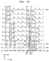
- display pulses 100 and 500 are periodically applied to all X electrode lines and all Y electrode lines.
- a reset step of initializing the discharge conditions of a previous sub-field and an address step of forming wall charges at discharge cells to be displayed in a current sub-field are sequentially performed during a time while the display pulses 100 and 500 are not applied.
- a bias pulse 900 which has the same polarity as and a lower voltage than the display pulses 100 and 500 is applied to all address electrode lines.
- the probability that space charges move from discharge cells where display discharging is provoked to adjacent otherwise discharge cells due to the display pulses 100 and 500 can be reduced.
- the probability that address discharging is provoked so as to form wall charges at discharge cells where it is not supposed that wall charges are formed at the address step can be reduced. Consequently, the accuracy of address discharging is increased in driving a plasma display panel according to an address-while-display driving method, thereby improving the picture quality of the plasma display panel and reducing the power consumption.
- address discharging may be performed at discharge cells where it is not supposed that wall charges are formed due to high potential of negative polarity of the Y electrodes of the discharge cells even if the data pulse 800 of positive polarity is not applied to the address electrodes thereof.
- undesired address discharging is provoked at unselected discharge cells, and wall charges of positive polarity are formed around the Y electrodes of the unselected discharge cells, so a succeeding application of the display pulse 500 may cause undesirable display discharging to be achieved.
- the bias pulse 900 having the same polarity as and a lower voltage than the display pulses 100 and 500 is applied to all the address electrode lines while the display pulses 100 and 500 are applied to all the X and Y electrode lines according to the driving method of FIG. 10, the probability that space charges move from discharge cells where display discharging is provoked to adjacent otherwise discharge cells due to the display pulses 100 and 500 can be reduced. This will be described in detail below.
- FIG. 12 illustrates driving signals applied during a minimum driving period according to the driving method of FIG. 10 in detail.
- a reference character S A1..n denotes a display data signal corresponding to a Y electrode line which is scanned
- a reference character S YGi denotes a driving signal applied to an i-th Y electrode line
- a reference character S XGi denotes a driving signal applied to an i-th X electrode line.
- Reference numeral 400 denotes a scan bias pulse which is applied to a Y electrode line
- reference numeral 500 denotes a display pulse
- reference numeral 600 denotes a scan pulse
- reference numeral 700 denotes a scan bias pulse which is applied to an X electrode line
- reference numeral 800 denotes a data pulse which is applied to selected address electrode lines.
- the bias pulse 900 having the same polarity and voltage as the display pulses 100 and 500 is applied to all the address electrode lines while the display pulses 100 and 500 are applied. Accordingly, display discharging is performed at selected discharge cells of a pair of i+1st X and Y electrode lines by the display pulse 100 of positive polarity which is applied to each Y electrode.
- the data pulse 800 of positive polarity is not applied to the address electrodes of discharge cells where it is not supposed that wall charges are formed, and potential of negative polarity of the Y electrodes of the discharge cells are not very high, so address discharging is not performed.
- undesired address discharging does not occur at unselected discharge cells, and wall charges of positive polarity are not formed around the Y electrodes of the unselected discharge cells, so a succeeding application of the display pulse 500 does not cause undesirable display discharging to be achieved.
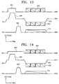
- FIG. 13 illustrates driving signals applied during a minimum driving period in a method according to a second embodiment of the present invention in detail.
- the same reference numerals denote the same functional elements.
- a bias pulse 901 of positive polarity is applied to all address electrode lines only while the display pulse 500 is applied to all Y electrode lines.
- the operation according to the driving method of FIG. 13 is the same as described with reference to FIG. 12.
- FIG. 14 illustrates driving signals applied during a minimum driving period in a method according to a third embodiment of the present invention in detail.
- the same reference numerals denote tie same functional elements.
- FIG. 14 is compared with FIGS. 12 and 13, a bias pulse 902 having the same polarity as and a lower voltage than the display pulse 500 is applied to all address electrode lines while the display pulses 500 are applied to all X and Y electrode lines.
- the operation according to the driving method of FIG. 14 is the same as described with reference to FIG. 12.
- a bias pulse having the same polarity as and a lower voltage than display pulses is applied to all address electrode lines while the display pulses are applied. Accordingly, the probability that space charges at discharge cells, where display discharging is provoked by the display pulses, move toward adjacent otherwise discharge cells can be reduced. In other words, the probability that address discharging is provoked so as to form wall charges at discharge cells where wall charges should not be formed at the address step can be reduced. Consequently, the accuracy of address discharging is increased in driving a plasma display panel according to an address-while-display driving method, thereby improving the picture quality of the plasma display panel and reducing the power consumption.
Landscapes
- Engineering & Computer Science (AREA)
- Physics & Mathematics (AREA)
- Power Engineering (AREA)
- Plasma & Fusion (AREA)
- Computer Hardware Design (AREA)
- General Physics & Mathematics (AREA)
- Theoretical Computer Science (AREA)
- Control Of Indicators Other Than Cathode Ray Tubes (AREA)
- Control Of Gas Discharge Display Tubes (AREA)
- Transforming Electric Information Into Light Information (AREA)
Abstract
Description
Claims (6)
- A method of driving a plasma display panel having front anc rear substrates which are spaced facing each other, X and Y electrode lines which are formed in parallel between the front and rear substrates, and address electrode lines formed to be perpendicular to the X and Y electrode lines so that discharge cells are defined by the crossing X and Y electrode lines and the address electrode lines, the method comprising the steps of periodically applying display pulses to all the X and Y electrode lines, and sequentially performing a reset step of initializing the discharge conditions of a previous sub-field and an address step of forming wall charges at discharge cells to be displayed in a current sub-field while the display pulses are not applied,
wherein a bias pulse having the same polarity as and a lower voltage than the display pulses is applied to all the address electrode lines while the display pulses are applied. - The method of claim 1, wherein the voltage of the bias pulse applied to all the address electrode lines is the same as or lower than the voltage of a data pulse which is applied to selected address electrode lines during the address step.
- The method of claim 1, wherein the bias pulse is applied to all the address electrode lines only while the display pulses are applied to all the Y electrode lines, and during the address step, a data pulse is applied to selected address electrode lines, and simultaneously, a scan pulse having polarity opposite to that of the data pulse is applied to a corresponding single Y electrode line so that wall charges are formed at discharge cells to be displayed.
- In a method of driving a plasma display panel having front and rear substrates which are spaced facing each other, X and Y electrode lines which are formed in parallel between the front and rear substrates, and address electrode lines formed to be perpendicular to the X and Y electrode lines so that discharge cells are defined by the crossing X and Y electrode lines and the address electrode lines, display pulses are periodically applied to all the X and Y electrode lines, and a reset step of initializing the discharge conditions of a previous sub-field and an address step of forming wall charges at discharge cells to be displayed in a current sub-field are sequentially performed while the display pulses are not applied,
the improvement being characterized in that a bias pulse having the same polarity as and a lower voltage than the display pulses is applied to all the address electrode lines while the display pulses are applied. - The method of claim 1, wherein the voltage of the bias pulse applied to all the address electrode lines is the same as or lower than the voltage of a data pulse which is applied to selected address electrode lines during the address step.
- The method of claim 1, wherein the bias pulse is applied to all the address electrode lines only while the display pulses are applied to all the Y electrode lines, and during the address step, a data pulse is applied to selected address electrode lines, and simultaneously, a scan pulse having polarity opposite to that of the data pulse is applied to a corresponding single Y electrode line so that wall charges are formed at discharge cells to be displayed.
Applications Claiming Priority (2)
| Application Number | Priority Date | Filing Date | Title |
|---|---|---|---|
| KR2000060256 | 2000-10-13 | ||
| KR1020000060256A KR100349923B1 (en) | 2000-10-13 | 2000-10-13 | Method for driving a plasma display panel |
Publications (2)
| Publication Number | Publication Date |
|---|---|
| EP1197941A2 true EP1197941A2 (en) | 2002-04-17 |
| EP1197941A3 EP1197941A3 (en) | 2003-12-10 |
Family
ID=19693314
Family Applications (1)
| Application Number | Title | Priority Date | Filing Date |
|---|---|---|---|
| EP01304028A Withdrawn EP1197941A3 (en) | 2000-10-13 | 2001-05-02 | Method for driving plasma display panel |
Country Status (5)
| Country | Link |
|---|---|
| US (1) | US6472826B2 (en) |
| EP (1) | EP1197941A3 (en) |
| JP (1) | JP2002132211A (en) |
| KR (1) | KR100349923B1 (en) |
| CN (1) | CN1276403C (en) |
Cited By (1)
| Publication number | Priority date | Publication date | Assignee | Title |
|---|---|---|---|---|
| CN100428299C (en) * | 2004-11-09 | 2008-10-22 | 三星Sdi株式会社 | Plasma display device and driving method for stable address discharge |
Families Citing this family (5)
| Publication number | Priority date | Publication date | Assignee | Title |
|---|---|---|---|---|
| KR100524306B1 (en) * | 2003-06-10 | 2005-10-28 | 엘지전자 주식회사 | Reset method and apparatus of plasma display panel |
| KR101022116B1 (en) * | 2004-03-05 | 2011-03-17 | 엘지전자 주식회사 | Plasma Display Panel Driving Method |
| KR100612234B1 (en) * | 2004-05-28 | 2006-08-11 | 삼성에스디아이 주식회사 | Plasma display device |
| US20090009436A1 (en) * | 2005-03-25 | 2009-01-08 | Keiji Akamatsu | Plasma display panel device and drive method thereof |
| WO2006103961A1 (en) * | 2005-03-25 | 2006-10-05 | Matsushita Electric Industrial Co., Ltd. | Plasma display panel device and drive method thereof |
Family Cites Families (9)
| Publication number | Priority date | Publication date | Assignee | Title |
|---|---|---|---|---|
| JP2932686B2 (en) * | 1990-11-28 | 1999-08-09 | 日本電気株式会社 | Driving method of plasma display panel |
| JP3259253B2 (en) * | 1990-11-28 | 2002-02-25 | 富士通株式会社 | Gray scale driving method and gray scale driving apparatus for flat display device |
| JP2772753B2 (en) * | 1993-12-10 | 1998-07-09 | 富士通株式会社 | Plasma display panel, driving method and driving circuit thereof |
| US5972499A (en) | 1997-06-04 | 1999-10-26 | Sterling Chemicals International, Inc. | Antistatic fibers and methods for making the same |
| KR100258913B1 (en) * | 1997-09-01 | 2000-06-15 | 손욱 | An ac plasma display panel and a driving method thereof |
| JP3421578B2 (en) * | 1998-06-11 | 2003-06-30 | 富士通株式会社 | Driving method of PDP |
| JP2000047634A (en) * | 1998-07-29 | 2000-02-18 | Pioneer Electron Corp | Driving method of plasma display device |
| EP1022713A3 (en) * | 1999-01-14 | 2000-12-06 | Nec Corporation | Method of driving AC-discharge plasma display panel |
| KR100284341B1 (en) * | 1999-03-02 | 2001-03-02 | 김순택 | Method for driving a plasma display panel |
-
2000
- 2000-10-13 KR KR1020000060256A patent/KR100349923B1/en not_active Expired - Fee Related
-
2001
- 2001-05-02 EP EP01304028A patent/EP1197941A3/en not_active Withdrawn
- 2001-05-04 US US09/848,342 patent/US6472826B2/en not_active Expired - Fee Related
- 2001-05-08 CN CNB011192240A patent/CN1276403C/en not_active Expired - Fee Related
- 2001-05-09 JP JP2001139183A patent/JP2002132211A/en active Pending
Cited By (1)
| Publication number | Priority date | Publication date | Assignee | Title |
|---|---|---|---|---|
| CN100428299C (en) * | 2004-11-09 | 2008-10-22 | 三星Sdi株式会社 | Plasma display device and driving method for stable address discharge |
Also Published As
| Publication number | Publication date |
|---|---|
| US20020043940A1 (en) | 2002-04-18 |
| JP2002132211A (en) | 2002-05-09 |
| KR20020029489A (en) | 2002-04-19 |
| EP1197941A3 (en) | 2003-12-10 |
| CN1276403C (en) | 2006-09-20 |
| US6472826B2 (en) | 2002-10-29 |
| KR100349923B1 (en) | 2002-08-24 |
| CN1349208A (en) | 2002-05-15 |
Similar Documents
| Publication | Publication Date | Title |
|---|---|---|
| JPH10247456A (en) | Plasma display panel, plasma display device, and method of driving plasma display panel | |
| US20060152446A1 (en) | Method of driving plasma display panel | |
| KR100388912B1 (en) | Method for resetting plasma display panel for improving contrast | |
| KR100603297B1 (en) | Panel driving method, panel driving device and display panel | |
| JP4089759B2 (en) | Driving method of AC type PDP | |
| US6975285B2 (en) | Plasma display panel and driving method thereof | |
| US7372434B2 (en) | Method of driving discharge display panel by address-display mixing | |
| KR100637240B1 (en) | Display panel with efficient pixel structure and its driving method | |
| US6472826B2 (en) | Method of driving plasma display panel and a plasma display device using the method | |
| US6603449B1 (en) | Method of addressing plasma panel with addresingpulses of variable widths | |
| KR100844834B1 (en) | Driving Method of Plasma Display Device | |
| KR100484113B1 (en) | Method of driving a plasma display panel | |
| US6693607B1 (en) | Method for driving plasma display panel with display discharge pulses having different power levels | |
| US6587085B2 (en) | Method of a driving plasma display panel | |
| US6765547B2 (en) | Method of driving a plasma display panel, and a plasma display apparatus using the method | |
| US20010011973A1 (en) | Method and apparatus for driving plasma display panel | |
| KR100313112B1 (en) | Method for driving plasma display panel | |
| KR100502341B1 (en) | Method for driving plasma display panel | |
| KR100603304B1 (en) | Panel driving method | |
| KR100647641B1 (en) | 플라즈마 Driving method of the plasma display panel without using the driving part | |
| KR100445028B1 (en) | Method of driving plasma display panel to prevent discharge from weakening in low gray-scale | |
| KR100811523B1 (en) | Plasma display device | |
| KR100313115B1 (en) | Method for driving plasma display panel | |
| JP3896817B2 (en) | Plasma display device | |
| KR100683672B1 (en) | Driving Method of Plasma Display Panel |
Legal Events
| Date | Code | Title | Description |
|---|---|---|---|
| PUAI | Public reference made under article 153(3) epc to a published international application that has entered the european phase |
Free format text: ORIGINAL CODE: 0009012 |
|
| AK | Designated contracting states |
Kind code of ref document: A2 Designated state(s): AT BE CH CY DE DK ES FI FR GB GR IE IT LI LU MC NL PT SE TR |
|
| AX | Request for extension of the european patent |
Free format text: AL;LT;LV;MK;RO;SI |
|
| PUAL | Search report despatched |
Free format text: ORIGINAL CODE: 0009013 |
|
| AK | Designated contracting states |
Kind code of ref document: A3 Designated state(s): AT BE CH CY DE DK ES FI FR GB GR IE IT LI LU MC NL PT SE TR |
|
| AX | Request for extension of the european patent |
Extension state: AL LT LV MK RO SI |
|
| 17P | Request for examination filed |
Effective date: 20040421 |
|
| AKX | Designation fees paid |
Designated state(s): DE FR GB |
|
| 17Q | First examination report despatched |
Effective date: 20070712 |
|
| STAA | Information on the status of an ep patent application or granted ep patent |
Free format text: STATUS: THE APPLICATION IS DEEMED TO BE WITHDRAWN |
|
| 18D | Application deemed to be withdrawn |
Effective date: 20091014 |