EP1197778A2 - Micro-electro-optical mechanical device having an implanted dopant included therein and a method of manufacture therefor - Google Patents
Micro-electro-optical mechanical device having an implanted dopant included therein and a method of manufacture therefor Download PDFInfo
- Publication number
- EP1197778A2 EP1197778A2 EP01308610A EP01308610A EP1197778A2 EP 1197778 A2 EP1197778 A2 EP 1197778A2 EP 01308610 A EP01308610 A EP 01308610A EP 01308610 A EP01308610 A EP 01308610A EP 1197778 A2 EP1197778 A2 EP 1197778A2
- Authority
- EP
- European Patent Office
- Prior art keywords
- light reflective
- recited
- mirror
- electro
- micro
- Prior art date
- Legal status (The legal status is an assumption and is not a legal conclusion. Google has not performed a legal analysis and makes no representation as to the accuracy of the status listed.)
- Granted
Links
- 239000002019 doping agent Substances 0.000 title claims abstract description 51
- 238000000034 method Methods 0.000 title claims description 29
- 238000004519 manufacturing process Methods 0.000 title claims description 11
- 230000003287 optical effect Effects 0.000 claims abstract description 184
- 239000000758 substrate Substances 0.000 claims abstract description 60
- 238000004891 communication Methods 0.000 claims description 26
- 238000005468 ion implantation Methods 0.000 claims description 26
- 239000000835 fiber Substances 0.000 claims description 22
- PCHJSUWPFVWCPO-UHFFFAOYSA-N gold Chemical compound [Au] PCHJSUWPFVWCPO-UHFFFAOYSA-N 0.000 claims description 21
- 229910052737 gold Inorganic materials 0.000 claims description 21
- 239000010931 gold Substances 0.000 claims description 21
- BASFCYQUMIYNBI-UHFFFAOYSA-N platinum Chemical compound [Pt] BASFCYQUMIYNBI-UHFFFAOYSA-N 0.000 claims description 18
- 239000000463 material Substances 0.000 claims description 16
- 239000007787 solid Substances 0.000 claims description 13
- BQCADISMDOOEFD-UHFFFAOYSA-N Silver Chemical compound [Ag] BQCADISMDOOEFD-UHFFFAOYSA-N 0.000 claims description 11
- 229910052782 aluminium Inorganic materials 0.000 claims description 11
- XAGFODPZIPBFFR-UHFFFAOYSA-N aluminium Chemical compound [Al] XAGFODPZIPBFFR-UHFFFAOYSA-N 0.000 claims description 11
- 230000008569 process Effects 0.000 claims description 11
- 229910052709 silver Inorganic materials 0.000 claims description 11
- 239000004332 silver Substances 0.000 claims description 11
- 238000010438 heat treatment Methods 0.000 claims description 10
- 229910052710 silicon Inorganic materials 0.000 claims description 10
- 239000010703 silicon Substances 0.000 claims description 10
- RYGMFSIKBFXOCR-UHFFFAOYSA-N Copper Chemical compound [Cu] RYGMFSIKBFXOCR-UHFFFAOYSA-N 0.000 claims description 9
- XUIMIQQOPSSXEZ-UHFFFAOYSA-N Silicon Chemical compound [Si] XUIMIQQOPSSXEZ-UHFFFAOYSA-N 0.000 claims description 9
- 229910052802 copper Inorganic materials 0.000 claims description 9
- 239000010949 copper Substances 0.000 claims description 9
- 229910052697 platinum Inorganic materials 0.000 claims description 9
- 229910052703 rhodium Inorganic materials 0.000 claims description 9
- 239000010948 rhodium Substances 0.000 claims description 9
- MHOVAHRLVXNVSD-UHFFFAOYSA-N rhodium atom Chemical compound [Rh] MHOVAHRLVXNVSD-UHFFFAOYSA-N 0.000 claims description 9
- 238000000605 extraction Methods 0.000 claims description 7
- VYPSYNLAJGMNEJ-UHFFFAOYSA-N Silicium dioxide Chemical compound O=[Si]=O VYPSYNLAJGMNEJ-UHFFFAOYSA-N 0.000 claims description 6
- 229910021420 polycrystalline silicon Inorganic materials 0.000 claims description 6
- 229920005591 polysilicon Polymers 0.000 claims description 6
- 229910052581 Si3N4 Inorganic materials 0.000 claims description 3
- 238000005229 chemical vapour deposition Methods 0.000 claims description 3
- 238000004070 electrodeposition Methods 0.000 claims description 3
- 238000001704 evaporation Methods 0.000 claims description 3
- 230000008020 evaporation Effects 0.000 claims description 3
- 238000003384 imaging method Methods 0.000 claims description 3
- 238000004544 sputter deposition Methods 0.000 claims description 3
- 229910003460 diamond Inorganic materials 0.000 claims description 2
- 239000010432 diamond Substances 0.000 claims description 2
- 238000001459 lithography Methods 0.000 claims description 2
- HBMJWWWQQXIZIP-UHFFFAOYSA-N silicon carbide Chemical compound [Si+]#[C-] HBMJWWWQQXIZIP-UHFFFAOYSA-N 0.000 claims description 2
- 229910010271 silicon carbide Inorganic materials 0.000 claims description 2
- HQVNEWCFYHHQES-UHFFFAOYSA-N silicon nitride Chemical compound N12[Si]34N5[Si]62N3[Si]51N64 HQVNEWCFYHHQES-UHFFFAOYSA-N 0.000 claims description 2
- 229910052814 silicon oxide Inorganic materials 0.000 claims description 2
- 229910021421 monocrystalline silicon Inorganic materials 0.000 claims 1
- 230000000149 penetrating effect Effects 0.000 claims 1
- 230000000717 retained effect Effects 0.000 claims 1
- 125000004429 atom Chemical group 0.000 description 27
- 150000002500 ions Chemical class 0.000 description 26
- 238000002513 implantation Methods 0.000 description 18
- 230000035515 penetration Effects 0.000 description 13
- 241000894007 species Species 0.000 description 13
- 229910052751 metal Inorganic materials 0.000 description 12
- 239000002184 metal Substances 0.000 description 12
- 230000008859 change Effects 0.000 description 10
- 239000010408 film Substances 0.000 description 10
- 230000001419 dependent effect Effects 0.000 description 9
- XKRFYHLGVUSROY-UHFFFAOYSA-N Argon Chemical compound [Ar] XKRFYHLGVUSROY-UHFFFAOYSA-N 0.000 description 6
- IJGRMHOSHXDMSA-UHFFFAOYSA-N Atomic nitrogen Chemical compound N#N IJGRMHOSHXDMSA-UHFFFAOYSA-N 0.000 description 6
- PXHVJJICTQNCMI-UHFFFAOYSA-N Nickel Chemical compound [Ni] PXHVJJICTQNCMI-UHFFFAOYSA-N 0.000 description 6
- KDLHZDBZIXYQEI-UHFFFAOYSA-N Palladium Chemical compound [Pd] KDLHZDBZIXYQEI-UHFFFAOYSA-N 0.000 description 6
- 230000000694 effects Effects 0.000 description 6
- 239000012528 membrane Substances 0.000 description 6
- 239000013307 optical fiber Substances 0.000 description 6
- 239000002245 particle Substances 0.000 description 6
- 238000001228 spectrum Methods 0.000 description 6
- 238000005728 strengthening Methods 0.000 description 6
- VYZAMTAEIAYCRO-UHFFFAOYSA-N Chromium Chemical compound [Cr] VYZAMTAEIAYCRO-UHFFFAOYSA-N 0.000 description 5
- RTAQQCXQSZGOHL-UHFFFAOYSA-N Titanium Chemical compound [Ti] RTAQQCXQSZGOHL-UHFFFAOYSA-N 0.000 description 5
- 229910052804 chromium Inorganic materials 0.000 description 5
- 239000011651 chromium Substances 0.000 description 5
- 239000002244 precipitate Substances 0.000 description 5
- 229910052761 rare earth metal Inorganic materials 0.000 description 5
- 230000002829 reductive effect Effects 0.000 description 5
- 230000003595 spectral effect Effects 0.000 description 5
- 230000006641 stabilisation Effects 0.000 description 5
- 238000011105 stabilization Methods 0.000 description 5
- 229910052719 titanium Inorganic materials 0.000 description 5
- 239000010936 titanium Substances 0.000 description 5
- 238000007514 turning Methods 0.000 description 5
- XEEYBQQBJWHFJM-UHFFFAOYSA-N Iron Chemical compound [Fe] XEEYBQQBJWHFJM-UHFFFAOYSA-N 0.000 description 4
- 229910052793 cadmium Inorganic materials 0.000 description 4
- BDOSMKKIYDKNTQ-UHFFFAOYSA-N cadmium atom Chemical compound [Cd] BDOSMKKIYDKNTQ-UHFFFAOYSA-N 0.000 description 4
- 239000007943 implant Substances 0.000 description 4
- 238000002310 reflectometry Methods 0.000 description 4
- ZOXJGFHDIHLPTG-UHFFFAOYSA-N Boron Chemical compound [B] ZOXJGFHDIHLPTG-UHFFFAOYSA-N 0.000 description 3
- OKTJSMMVPCPJKN-UHFFFAOYSA-N Carbon Chemical compound [C] OKTJSMMVPCPJKN-UHFFFAOYSA-N 0.000 description 3
- 229910052684 Cerium Inorganic materials 0.000 description 3
- ZAMOUSCENKQFHK-UHFFFAOYSA-N Chlorine atom Chemical compound [Cl] ZAMOUSCENKQFHK-UHFFFAOYSA-N 0.000 description 3
- 229910052692 Dysprosium Inorganic materials 0.000 description 3
- 229910052691 Erbium Inorganic materials 0.000 description 3
- 229910052693 Europium Inorganic materials 0.000 description 3
- 229910052688 Gadolinium Inorganic materials 0.000 description 3
- GYHNNYVSQQEPJS-UHFFFAOYSA-N Gallium Chemical compound [Ga] GYHNNYVSQQEPJS-UHFFFAOYSA-N 0.000 description 3
- 229910052689 Holmium Inorganic materials 0.000 description 3
- WHXSMMKQMYFTQS-UHFFFAOYSA-N Lithium Chemical compound [Li] WHXSMMKQMYFTQS-UHFFFAOYSA-N 0.000 description 3
- 229910052765 Lutetium Inorganic materials 0.000 description 3
- FYYHWMGAXLPEAU-UHFFFAOYSA-N Magnesium Chemical compound [Mg] FYYHWMGAXLPEAU-UHFFFAOYSA-N 0.000 description 3
- ZOKXTWBITQBERF-UHFFFAOYSA-N Molybdenum Chemical compound [Mo] ZOKXTWBITQBERF-UHFFFAOYSA-N 0.000 description 3
- 229910052779 Neodymium Inorganic materials 0.000 description 3
- KJTLSVCANCCWHF-UHFFFAOYSA-N Ruthenium Chemical compound [Ru] KJTLSVCANCCWHF-UHFFFAOYSA-N 0.000 description 3
- 229910052772 Samarium Inorganic materials 0.000 description 3
- BUGBHKTXTAQXES-UHFFFAOYSA-N Selenium Chemical compound [Se] BUGBHKTXTAQXES-UHFFFAOYSA-N 0.000 description 3
- NINIDFKCEFEMDL-UHFFFAOYSA-N Sulfur Chemical compound [S] NINIDFKCEFEMDL-UHFFFAOYSA-N 0.000 description 3
- 229910052771 Terbium Chemical group 0.000 description 3
- ATJFFYVFTNAWJD-UHFFFAOYSA-N Tin Chemical compound [Sn] ATJFFYVFTNAWJD-UHFFFAOYSA-N 0.000 description 3
- 229910052769 Ytterbium Inorganic materials 0.000 description 3
- HCHKCACWOHOZIP-UHFFFAOYSA-N Zinc Chemical compound [Zn] HCHKCACWOHOZIP-UHFFFAOYSA-N 0.000 description 3
- 238000000137 annealing Methods 0.000 description 3
- 229910052787 antimony Inorganic materials 0.000 description 3
- WATWJIUSRGPENY-UHFFFAOYSA-N antimony atom Chemical compound [Sb] WATWJIUSRGPENY-UHFFFAOYSA-N 0.000 description 3
- 229910052786 argon Inorganic materials 0.000 description 3
- QVGXLLKOCUKJST-UHFFFAOYSA-N atomic oxygen Chemical compound [O] QVGXLLKOCUKJST-UHFFFAOYSA-N 0.000 description 3
- 229910052788 barium Inorganic materials 0.000 description 3
- DSAJWYNOEDNPEQ-UHFFFAOYSA-N barium atom Chemical compound [Ba] DSAJWYNOEDNPEQ-UHFFFAOYSA-N 0.000 description 3
- 229910052797 bismuth Inorganic materials 0.000 description 3
- JCXGWMGPZLAOME-UHFFFAOYSA-N bismuth atom Chemical compound [Bi] JCXGWMGPZLAOME-UHFFFAOYSA-N 0.000 description 3
- 229910052796 boron Inorganic materials 0.000 description 3
- 229910052799 carbon Inorganic materials 0.000 description 3
- ZMIGMASIKSOYAM-UHFFFAOYSA-N cerium Chemical group [Ce][Ce][Ce][Ce][Ce][Ce][Ce][Ce][Ce][Ce][Ce][Ce][Ce][Ce][Ce][Ce][Ce][Ce][Ce][Ce][Ce][Ce][Ce][Ce][Ce][Ce][Ce][Ce][Ce][Ce][Ce][Ce][Ce][Ce][Ce][Ce][Ce][Ce] ZMIGMASIKSOYAM-UHFFFAOYSA-N 0.000 description 3
- 229910052801 chlorine Inorganic materials 0.000 description 3
- 239000000460 chlorine Substances 0.000 description 3
- 229910017052 cobalt Inorganic materials 0.000 description 3
- 239000010941 cobalt Substances 0.000 description 3
- GUTLYIVDDKVIGB-UHFFFAOYSA-N cobalt atom Chemical compound [Co] GUTLYIVDDKVIGB-UHFFFAOYSA-N 0.000 description 3
- 238000001816 cooling Methods 0.000 description 3
- 230000007547 defect Effects 0.000 description 3
- 238000013461 design Methods 0.000 description 3
- KBQHZAAAGSGFKK-UHFFFAOYSA-N dysprosium atom Chemical compound [Dy] KBQHZAAAGSGFKK-UHFFFAOYSA-N 0.000 description 3
- UYAHIZSMUZPPFV-UHFFFAOYSA-N erbium Chemical group [Er] UYAHIZSMUZPPFV-UHFFFAOYSA-N 0.000 description 3
- OGPBJKLSAFTDLK-UHFFFAOYSA-N europium atom Chemical group [Eu] OGPBJKLSAFTDLK-UHFFFAOYSA-N 0.000 description 3
- UIWYJDYFSGRHKR-UHFFFAOYSA-N gadolinium atom Chemical compound [Gd] UIWYJDYFSGRHKR-UHFFFAOYSA-N 0.000 description 3
- 229910052733 gallium Inorganic materials 0.000 description 3
- 229910052734 helium Inorganic materials 0.000 description 3
- 239000001307 helium Substances 0.000 description 3
- SWQJXJOGLNCZEY-UHFFFAOYSA-N helium atom Chemical compound [He] SWQJXJOGLNCZEY-UHFFFAOYSA-N 0.000 description 3
- KJZYNXUDTRRSPN-UHFFFAOYSA-N holmium atom Chemical compound [Ho] KJZYNXUDTRRSPN-UHFFFAOYSA-N 0.000 description 3
- BHEPBYXIRTUNPN-UHFFFAOYSA-N hydridophosphorus(.) (triplet) Chemical compound [PH] BHEPBYXIRTUNPN-UHFFFAOYSA-N 0.000 description 3
- 239000001257 hydrogen Substances 0.000 description 3
- 229910052739 hydrogen Inorganic materials 0.000 description 3
- 229910052738 indium Inorganic materials 0.000 description 3
- APFVFJFRJDLVQX-UHFFFAOYSA-N indium atom Chemical compound [In] APFVFJFRJDLVQX-UHFFFAOYSA-N 0.000 description 3
- 229910052741 iridium Inorganic materials 0.000 description 3
- GKOZUEZYRPOHIO-UHFFFAOYSA-N iridium atom Chemical compound [Ir] GKOZUEZYRPOHIO-UHFFFAOYSA-N 0.000 description 3
- 229910052743 krypton Inorganic materials 0.000 description 3
- DNNSSWSSYDEUBZ-UHFFFAOYSA-N krypton atom Chemical compound [Kr] DNNSSWSSYDEUBZ-UHFFFAOYSA-N 0.000 description 3
- 229910052746 lanthanum Inorganic materials 0.000 description 3
- FZLIPJUXYLNCLC-UHFFFAOYSA-N lanthanum atom Chemical group [La] FZLIPJUXYLNCLC-UHFFFAOYSA-N 0.000 description 3
- 229910052744 lithium Inorganic materials 0.000 description 3
- OHSVLFRHMCKCQY-UHFFFAOYSA-N lutetium atom Chemical compound [Lu] OHSVLFRHMCKCQY-UHFFFAOYSA-N 0.000 description 3
- 229910052749 magnesium Inorganic materials 0.000 description 3
- 239000011777 magnesium Substances 0.000 description 3
- WPBNNNQJVZRUHP-UHFFFAOYSA-L manganese(2+);methyl n-[[2-(methoxycarbonylcarbamothioylamino)phenyl]carbamothioyl]carbamate;n-[2-(sulfidocarbothioylamino)ethyl]carbamodithioate Chemical compound [Mn+2].[S-]C(=S)NCCNC([S-])=S.COC(=O)NC(=S)NC1=CC=CC=C1NC(=S)NC(=O)OC WPBNNNQJVZRUHP-UHFFFAOYSA-L 0.000 description 3
- 229910052750 molybdenum Inorganic materials 0.000 description 3
- 239000011733 molybdenum Substances 0.000 description 3
- QEFYFXOXNSNQGX-UHFFFAOYSA-N neodymium atom Chemical group [Nd] QEFYFXOXNSNQGX-UHFFFAOYSA-N 0.000 description 3
- 229910052754 neon Inorganic materials 0.000 description 3
- GKAOGPIIYCISHV-UHFFFAOYSA-N neon atom Chemical compound [Ne] GKAOGPIIYCISHV-UHFFFAOYSA-N 0.000 description 3
- 229910052759 nickel Inorganic materials 0.000 description 3
- 229910052758 niobium Inorganic materials 0.000 description 3
- 239000010955 niobium Substances 0.000 description 3
- GUCVJGMIXFAOAE-UHFFFAOYSA-N niobium atom Chemical compound [Nb] GUCVJGMIXFAOAE-UHFFFAOYSA-N 0.000 description 3
- 229910052757 nitrogen Inorganic materials 0.000 description 3
- 239000001301 oxygen Substances 0.000 description 3
- 229910052760 oxygen Inorganic materials 0.000 description 3
- 229910052763 palladium Inorganic materials 0.000 description 3
- 230000000737 periodic effect Effects 0.000 description 3
- 238000012545 processing Methods 0.000 description 3
- 229910052702 rhenium Inorganic materials 0.000 description 3
- WUAPFZMCVAUBPE-UHFFFAOYSA-N rhenium atom Chemical compound [Re] WUAPFZMCVAUBPE-UHFFFAOYSA-N 0.000 description 3
- 229910052707 ruthenium Inorganic materials 0.000 description 3
- KZUNJOHGWZRPMI-UHFFFAOYSA-N samarium atom Chemical group [Sm] KZUNJOHGWZRPMI-UHFFFAOYSA-N 0.000 description 3
- 229910052706 scandium Inorganic materials 0.000 description 3
- SIXSYDAISGFNSX-UHFFFAOYSA-N scandium atom Chemical compound [Sc] SIXSYDAISGFNSX-UHFFFAOYSA-N 0.000 description 3
- 229910052711 selenium Inorganic materials 0.000 description 3
- 239000011669 selenium Substances 0.000 description 3
- 229910052712 strontium Inorganic materials 0.000 description 3
- CIOAGBVUUVVLOB-UHFFFAOYSA-N strontium atom Chemical compound [Sr] CIOAGBVUUVVLOB-UHFFFAOYSA-N 0.000 description 3
- 229910052717 sulfur Inorganic materials 0.000 description 3
- 239000011593 sulfur Substances 0.000 description 3
- 229910052714 tellurium Inorganic materials 0.000 description 3
- PORWMNRCUJJQNO-UHFFFAOYSA-N tellurium atom Chemical compound [Te] PORWMNRCUJJQNO-UHFFFAOYSA-N 0.000 description 3
- GZCRRIHWUXGPOV-UHFFFAOYSA-N terbium atom Chemical group [Tb] GZCRRIHWUXGPOV-UHFFFAOYSA-N 0.000 description 3
- 229910052718 tin Inorganic materials 0.000 description 3
- WFKWXMTUELFFGS-UHFFFAOYSA-N tungsten Chemical compound [W] WFKWXMTUELFFGS-UHFFFAOYSA-N 0.000 description 3
- 229910052721 tungsten Inorganic materials 0.000 description 3
- 239000010937 tungsten Substances 0.000 description 3
- 229910052720 vanadium Inorganic materials 0.000 description 3
- GPPXJZIENCGNKB-UHFFFAOYSA-N vanadium Chemical compound [V]#[V] GPPXJZIENCGNKB-UHFFFAOYSA-N 0.000 description 3
- NAWDYIZEMPQZHO-UHFFFAOYSA-N ytterbium Chemical compound [Yb] NAWDYIZEMPQZHO-UHFFFAOYSA-N 0.000 description 3
- 229910052725 zinc Inorganic materials 0.000 description 3
- 239000011701 zinc Substances 0.000 description 3
- PXGOKWXKJXAPGV-UHFFFAOYSA-N Fluorine Chemical compound FF PXGOKWXKJXAPGV-UHFFFAOYSA-N 0.000 description 2
- UFHFLCQGNIYNRP-UHFFFAOYSA-N Hydrogen Chemical compound [H][H] UFHFLCQGNIYNRP-UHFFFAOYSA-N 0.000 description 2
- DGAQECJNVWCQMB-PUAWFVPOSA-M Ilexoside XXIX Chemical compound C[C@@H]1CC[C@@]2(CC[C@@]3(C(=CC[C@H]4[C@]3(CC[C@@H]5[C@@]4(CC[C@@H](C5(C)C)OS(=O)(=O)[O-])C)C)[C@@H]2[C@]1(C)O)C)C(=O)O[C@H]6[C@@H]([C@H]([C@@H]([C@H](O6)CO)O)O)O.[Na+] DGAQECJNVWCQMB-PUAWFVPOSA-M 0.000 description 2
- ZLMJMSJWJFRBEC-UHFFFAOYSA-N Potassium Chemical compound [K] ZLMJMSJWJFRBEC-UHFFFAOYSA-N 0.000 description 2
- QCWXUUIWCKQGHC-UHFFFAOYSA-N Zirconium Chemical compound [Zr] QCWXUUIWCKQGHC-UHFFFAOYSA-N 0.000 description 2
- 238000003491 array Methods 0.000 description 2
- 230000015572 biosynthetic process Effects 0.000 description 2
- 229910052681 coesite Inorganic materials 0.000 description 2
- 230000008878 coupling Effects 0.000 description 2
- 238000010168 coupling process Methods 0.000 description 2
- 238000005859 coupling reaction Methods 0.000 description 2
- 229910052906 cristobalite Inorganic materials 0.000 description 2
- 239000013078 crystal Substances 0.000 description 2
- 239000011737 fluorine Substances 0.000 description 2
- 229910052731 fluorine Inorganic materials 0.000 description 2
- 229910052732 germanium Inorganic materials 0.000 description 2
- GNPVGFCGXDBREM-UHFFFAOYSA-N germanium atom Chemical compound [Ge] GNPVGFCGXDBREM-UHFFFAOYSA-N 0.000 description 2
- 229910052735 hafnium Inorganic materials 0.000 description 2
- VBJZVLUMGGDVMO-UHFFFAOYSA-N hafnium atom Chemical compound [Hf] VBJZVLUMGGDVMO-UHFFFAOYSA-N 0.000 description 2
- 238000003780 insertion Methods 0.000 description 2
- 230000037431 insertion Effects 0.000 description 2
- 229910000765 intermetallic Inorganic materials 0.000 description 2
- 229910052742 iron Inorganic materials 0.000 description 2
- 239000011133 lead Substances 0.000 description 2
- 230000000873 masking effect Effects 0.000 description 2
- 239000011159 matrix material Substances 0.000 description 2
- 230000004048 modification Effects 0.000 description 2
- 238000012986 modification Methods 0.000 description 2
- 230000006855 networking Effects 0.000 description 2
- 238000001579 optical reflectometry Methods 0.000 description 2
- 229910052700 potassium Inorganic materials 0.000 description 2
- 239000011591 potassium Substances 0.000 description 2
- 150000002910 rare earth metals Chemical group 0.000 description 2
- 230000004044 response Effects 0.000 description 2
- 229910052701 rubidium Inorganic materials 0.000 description 2
- IGLNJRXAVVLDKE-UHFFFAOYSA-N rubidium atom Chemical compound [Rb] IGLNJRXAVVLDKE-UHFFFAOYSA-N 0.000 description 2
- 238000000926 separation method Methods 0.000 description 2
- 238000007493 shaping process Methods 0.000 description 2
- 239000000377 silicon dioxide Substances 0.000 description 2
- 229910052708 sodium Inorganic materials 0.000 description 2
- 239000011734 sodium Substances 0.000 description 2
- 229910052682 stishovite Inorganic materials 0.000 description 2
- 229910052715 tantalum Inorganic materials 0.000 description 2
- GUVRBAGPIYLISA-UHFFFAOYSA-N tantalum atom Chemical compound [Ta] GUVRBAGPIYLISA-UHFFFAOYSA-N 0.000 description 2
- 238000007736 thin film deposition technique Methods 0.000 description 2
- 229910052905 tridymite Inorganic materials 0.000 description 2
- 229910052727 yttrium Inorganic materials 0.000 description 2
- VWQVUPCCIRVNHF-UHFFFAOYSA-N yttrium atom Chemical compound [Y] VWQVUPCCIRVNHF-UHFFFAOYSA-N 0.000 description 2
- 229910052726 zirconium Inorganic materials 0.000 description 2
- ZCYVEMRRCGMTRW-UHFFFAOYSA-N 7553-56-2 Chemical compound [I] ZCYVEMRRCGMTRW-UHFFFAOYSA-N 0.000 description 1
- -1 Silicon ion Chemical class 0.000 description 1
- 238000010521 absorption reaction Methods 0.000 description 1
- 238000005275 alloying Methods 0.000 description 1
- 230000004075 alteration Effects 0.000 description 1
- 230000002238 attenuated effect Effects 0.000 description 1
- 238000005452 bending Methods 0.000 description 1
- 230000009286 beneficial effect Effects 0.000 description 1
- 230000000903 blocking effect Effects 0.000 description 1
- 238000006243 chemical reaction Methods 0.000 description 1
- 238000005253 cladding Methods 0.000 description 1
- 230000000052 comparative effect Effects 0.000 description 1
- 238000010276 construction Methods 0.000 description 1
- 230000007812 deficiency Effects 0.000 description 1
- 230000002939 deleterious effect Effects 0.000 description 1
- 238000000151 deposition Methods 0.000 description 1
- 230000008021 deposition Effects 0.000 description 1
- 238000011161 development Methods 0.000 description 1
- 230000003467 diminishing effect Effects 0.000 description 1
- 238000005516 engineering process Methods 0.000 description 1
- 238000005530 etching Methods 0.000 description 1
- 239000007789 gas Chemical group 0.000 description 1
- 150000002431 hydrogen Chemical class 0.000 description 1
- 239000012535 impurity Substances 0.000 description 1
- 238000010348 incorporation Methods 0.000 description 1
- 239000011261 inert gas Substances 0.000 description 1
- PNDPGZBMCMUPRI-UHFFFAOYSA-N iodine Chemical compound II PNDPGZBMCMUPRI-UHFFFAOYSA-N 0.000 description 1
- 229910052740 iodine Inorganic materials 0.000 description 1
- 239000011630 iodine Substances 0.000 description 1
- 230000000670 limiting effect Effects 0.000 description 1
- 230000007246 mechanism Effects 0.000 description 1
- 239000007769 metal material Substances 0.000 description 1
- 238000005459 micromachining Methods 0.000 description 1
- 229910052762 osmium Inorganic materials 0.000 description 1
- SYQBFIAQOQZEGI-UHFFFAOYSA-N osmium atom Chemical compound [Os] SYQBFIAQOQZEGI-UHFFFAOYSA-N 0.000 description 1
- 238000000059 patterning Methods 0.000 description 1
- 230000010287 polarization Effects 0.000 description 1
- 238000001556 precipitation Methods 0.000 description 1
- 238000004881 precipitation hardening Methods 0.000 description 1
- 239000000047 product Substances 0.000 description 1
- 230000009467 reduction Effects 0.000 description 1
- 238000003860 storage Methods 0.000 description 1
- 238000006467 substitution reaction Methods 0.000 description 1
- 238000012360 testing method Methods 0.000 description 1
- 238000005382 thermal cycling Methods 0.000 description 1
- 239000010409 thin film Substances 0.000 description 1
- 230000036962 time dependent Effects 0.000 description 1
- 239000011135 tin Substances 0.000 description 1
- 229910052723 transition metal Inorganic materials 0.000 description 1
- 150000003624 transition metals Chemical class 0.000 description 1
- XLYOFNOQVPJJNP-UHFFFAOYSA-N water Substances O XLYOFNOQVPJJNP-UHFFFAOYSA-N 0.000 description 1
Images



Classifications
-
- G—PHYSICS
- G02—OPTICS
- G02B—OPTICAL ELEMENTS, SYSTEMS OR APPARATUS
- G02B26/00—Optical devices or arrangements for the control of light using movable or deformable optical elements
- G02B26/08—Optical devices or arrangements for the control of light using movable or deformable optical elements for controlling the direction of light
- G02B26/0816—Optical devices or arrangements for the control of light using movable or deformable optical elements for controlling the direction of light by means of one or more reflecting elements
- G02B26/0833—Optical devices or arrangements for the control of light using movable or deformable optical elements for controlling the direction of light by means of one or more reflecting elements the reflecting element being a micromechanical device, e.g. a MEMS mirror, DMD
- G02B26/0841—Optical devices or arrangements for the control of light using movable or deformable optical elements for controlling the direction of light by means of one or more reflecting elements the reflecting element being a micromechanical device, e.g. a MEMS mirror, DMD the reflecting element being moved or deformed by electrostatic means
-
- B—PERFORMING OPERATIONS; TRANSPORTING
- B81—MICROSTRUCTURAL TECHNOLOGY
- B81C—PROCESSES OR APPARATUS SPECIALLY ADAPTED FOR THE MANUFACTURE OR TREATMENT OF MICROSTRUCTURAL DEVICES OR SYSTEMS
- B81C1/00—Manufacture or treatment of devices or systems in or on a substrate
- B81C1/00642—Manufacture or treatment of devices or systems in or on a substrate for improving the physical properties of a device
- B81C1/0065—Mechanical properties
- B81C1/00666—Treatments for controlling internal stress or strain in MEMS structures
-
- G—PHYSICS
- G02—OPTICS
- G02B—OPTICAL ELEMENTS, SYSTEMS OR APPARATUS
- G02B6/00—Light guides; Structural details of arrangements comprising light guides and other optical elements, e.g. couplings
- G02B6/10—Light guides; Structural details of arrangements comprising light guides and other optical elements, e.g. couplings of the optical waveguide type
- G02B6/12—Light guides; Structural details of arrangements comprising light guides and other optical elements, e.g. couplings of the optical waveguide type of the integrated circuit kind
- G02B6/122—Basic optical elements, e.g. light-guiding paths
-
- G—PHYSICS
- G02—OPTICS
- G02B—OPTICAL ELEMENTS, SYSTEMS OR APPARATUS
- G02B6/00—Light guides; Structural details of arrangements comprising light guides and other optical elements, e.g. couplings
- G02B6/24—Coupling light guides
- G02B6/26—Optical coupling means
- G02B6/264—Optical coupling means with optical elements between opposed fibre ends which perform a function other than beam splitting
- G02B6/266—Optical coupling means with optical elements between opposed fibre ends which perform a function other than beam splitting the optical element being an attenuator
-
- B—PERFORMING OPERATIONS; TRANSPORTING
- B81—MICROSTRUCTURAL TECHNOLOGY
- B81B—MICROSTRUCTURAL DEVICES OR SYSTEMS, e.g. MICROMECHANICAL DEVICES
- B81B2201/00—Specific applications of microelectromechanical systems
- B81B2201/04—Optical MEMS
- B81B2201/042—Micromirrors, not used as optical switches
-
- B—PERFORMING OPERATIONS; TRANSPORTING
- B81—MICROSTRUCTURAL TECHNOLOGY
- B81B—MICROSTRUCTURAL DEVICES OR SYSTEMS, e.g. MICROMECHANICAL DEVICES
- B81B2203/00—Basic microelectromechanical structures
- B81B2203/01—Suspended structures, i.e. structures allowing a movement
- B81B2203/0127—Diaphragms, i.e. structures separating two media that can control the passage from one medium to another; Membranes, i.e. diaphragms with filtering function
-
- B—PERFORMING OPERATIONS; TRANSPORTING
- B81—MICROSTRUCTURAL TECHNOLOGY
- B81C—PROCESSES OR APPARATUS SPECIALLY ADAPTED FOR THE MANUFACTURE OR TREATMENT OF MICROSTRUCTURAL DEVICES OR SYSTEMS
- B81C2201/00—Manufacture or treatment of microstructural devices or systems
- B81C2201/01—Manufacture or treatment of microstructural devices or systems in or on a substrate
- B81C2201/0161—Controlling physical properties of the material
- B81C2201/0163—Controlling internal stress of deposited layers
- B81C2201/0164—Controlling internal stress of deposited layers by doping the layer
-
- G—PHYSICS
- G02—OPTICS
- G02B—OPTICAL ELEMENTS, SYSTEMS OR APPARATUS
- G02B6/00—Light guides; Structural details of arrangements comprising light guides and other optical elements, e.g. couplings
- G02B6/10—Light guides; Structural details of arrangements comprising light guides and other optical elements, e.g. couplings of the optical waveguide type
- G02B6/12—Light guides; Structural details of arrangements comprising light guides and other optical elements, e.g. couplings of the optical waveguide type of the integrated circuit kind
- G02B2006/12083—Constructional arrangements
- G02B2006/12104—Mirror; Reflectors or the like
Definitions
- the present invention is directed, in general, to an optical device and, more specifically, to a micro-electro-optical mechanical device having an implanted dopant included therein and a method of manufacture therefor.
- Optical communication systems typically include a variety of optical devices, for example, light sources, photo detectors, switches, cross connects, attenuators, mirrors, amplifiers, and filters.
- the optical devices transmit optical signals in the optical communications systems.
- Some optical devices are coupled to electro-mechanical structures, such as thermal actuators, forming an electro-mechanical optical device.
- electro-mechanical structure refers to a structure which moves mechanically under the control of an electrical signal.
- Some electro-mechanical structures move the optical devices from a predetermined first position to a predetermined second position.
- Cowan William D., et al. "Vertical Thermal Actuators for Micro-Opto-Electro-Mechanical Systems," SPIE, Vol. 3226, pp. 137-146 (1997), describes one such electro-mechanical structure useful for moving optical devices from the predetermined first positions to the predetermined second positions.
- MEMS optical devices often employ a periodic array of micro-machined mirrors, each mirror being individually movable in response to an electrical signal.
- the mirrors can each be cantilevered and moved by an electrostatic, piezoelectric, magnetic, or thermal actuation. See articles by L. Y. Lin, et al., IEEE Photonics Technology Lett. Vol. 10, p. 525, 1998, R. A. Miller, et al. Optical Engineering Vol. 36, p. 1399, 1997, and by J. W.
- the mirrors used in these optical devices are typically made up of a material which reflects light with high reflectivity at the desired operating wavelength of the light, for example at about the 1000 - 1600 nm wavelength range for the SiO 2 optical fiber-based telecommunication systems.
- Some examples of such reflective materials are gold, silver, rhodium, platinum, copper or aluminum.
- These reflective metal films typically have a thickness ranging from about 20 nm to about 2000 nm, and are deposited on a movable membrane substrate such as a silicon substrate. At least one adhesion-promoting bond layer is desirably added between the reflecting film and the substrate in order to prevent the reflecting film from getting peeled off.
- the fabrication of movable membrane structure in MEMS devices is well established and is typically based on silicon wafer processing.
- dimensional problems in the MEMS mirror structure caused by the stress include: i) undesirable bowing of the mirror substrate (membrane), which results in a non-focused or non-parallel light reflection and an increased loss of optical signal, ii) time-dependent change in mirror curvature due to the creep or stress relaxation in the reflective metal film, bond layer or the membrane substrate, iii) temperature-dependent change in mirror curvature due to the altered stress states and altered CTE mismatch conditions in the metal film, bond layer, and membrane substrate materials with changing temperature.
- the present invention provides a micro-electro-mechanical system (MEMS) optical device.
- MEMS micro-electro-mechanical system
- MEMS micro-electro-mechanical system
- MEMS micro-electro-mechanical system
- an optical communications system comprising:
- the inclusion of the implanted dopant within the light reflective optical layer increases the tensile stress of the device and tends to correct the concave curvature of the mirror structure toward a desirably flat configuration.
- the optical device 100 includes a mirror 110 and a mounting substrate 120, on which the mirror 110 is moveably mounted.
- the mirror 110 comprises a light reflective optical layer 130 formed over a substrate 140.
- the light reflective optical layer 130 has a dopant 150 located therein. The inclusion of the implanted dopant 150 within the light reflective optical layer 130, and optionally the substrate 140, helps to substantially reduce initial mirror curvature.
- the inclusion of the implanted dopant 150 within the light reflective optical layer 130, and optionally the substrate 140, also helps to substantially decrease the time or temperature-dependent changes of mirror curvature, such that the signal loss during operation of the micro-electro-mechanical system optical device 100, is minimized.
- temperatures, atomic percentage and numerous dopents that are set forth herein are exemplary only, and the present invention is not intended to be limited to such temperatures, percentages or atomic species, but may vary, depending on the embodiment.
- FIGURE 2 illustrates a cross-sectional view of a partially completed MEMS optical device 200, including a minor substrate 210.
- the mirror substrate 210 is a polysilicon substrate, however, it should be noted that other similar substrates known to those who are skilled in the art could be used.
- a poly silicon, singe crystal silicon, silicon nitride, silicon carbide, silicon oxide, diamond film, or any regional or layered combination of these materials may be used as the mirror substrate 210.
- the adhesion layer 220 may be formed using many processes, including known thin film deposition methods such as evaporation, sputtering, electrochemical deposition, or chemical vapor deposition.
- the adhesion layer 220 comprises titanium or chromium; however, the adhesion layer 220 is not limited to titanium or chromium, and other materials are within the scope of the present invention. It should be noted that using the adhesion layer 220 is desirable because it helps to bond the mirror substrate 210 and a subsequently formed light reflective optical layer together. However, it should also be noted that it is not required for the micro-electro-mechanical system optical device 200 to operate.
- the light reflective optical layer 310 is formed directly on the adhesion layer 220, which is formed directly on the mirror substrate 210.
- the light reflective optical layer 310 may comprise any material that is generally known to reflect light.
- the light reflective optical layer 310 is a metal light reflective optical layer.
- the metal may comprise any metallic material that reflects light with high reflectivity.
- the light reflective optical layer 310 may comprise gold, silver, rhodium, platinum, copper or aluminum.
- the light reflective optical layer 310 may be formed using many processes.
- the light reflective optical layer 31C can be deposited by known thin film deposition methods such as evaporation, sputtering, electrochemical deposition, or chemical vapor deposition.
- the light reflective optical layer 310 is typically formed to a thickness ranging from about 20 nm to about 2000 nm.
- FIGURE 4 illustrated is the partially completed MEMS optical device 200 illustrated in FIGURE 3, after implanting a dopant 410 (e.g., atomic species) within the light reflective optical layer 310.
- implanting may include dopants implanted by ion implantation, or in other embodiments, may include dopants positioned within the substrate by other doping processes.
- a blanket ion implantation process, or a shadow mask or lithographic patterning process could be used to implant the entire light reflective optical layer 310 or preselected regions of the light reflective optical layer 310.
- the dopant 410 is also located at least partially within the mirror substrate 210.
- the dopant 410 may be present as isolated embedded atoms in the light reflective optical layer 310, and mirror substrate 210 if included therein.
- the dopant 410 can be present as clusters or precipitates in the size range of about 1 nm to about 1000 nm, and preferably in the range from about 1 nm to about 100 nm.
- the introduction of optimally larger dopant 410 particles, most preferably having an average diameter ranging from about 5 nm to about 50 nm, can be facilitated by optional, post-implantation heat treatments. These sizes may enhance the precipitation strengthening effect, as the plastic deformation by dislocation movement becomes more difficult near the optimized particle size.
- the precipitates may comprise the implanted atoms only, or possibly the atoms of the host material, as well if intermetallic compounds can be formed.
- the implanted dopant may be selected from many elements in the periodic table. For the sake of maximum strengthening, preferred elements are those with minimum solid solubility in the light reflective optical layer 310, and mirror substrate 210 if included therein.
- the desired solid solubility of the dopant at about 300°C or less may be less than about 3 atomic percent, preferably less than about 1 atomic percent, and even more preferably less than about 0.3 atomic percent.
- the type of dopant 150 is preferably selected depending on the light reflective optical layer 310 used, for example gold, silver, rhodium, platinum, copper or aluminum.
- the desired dopant species should have a solid solubility of less than about 1 atomic percent, and preferably less than about 0.3 atomic percent at temperatures of about 300°C.
- Dopants that accommodate this small solid solubility include some substitutional elements, which in principle substantially takes up the lattice atom position in the gold light reflective optical layer 310, such as silicon, bismuth, strontium, barium, cadmium, tungsten, iridium, rhenium, rhodium, ruthenium, cobalt, sulfur, selenium, tellurium, chlorine, iodine and phosphorous.
- dopants that accommodate the desired small solid solubility include some selected elements in the rare earth group, such as cerium, europium, erbium, lanthanum, neodymium, samarium, and terbium, and gas atoms such as helium, neon, argon and krypton.
- the desired implantable species with desirably very little solid solubility in gold include boron, carbon, nitrogen, oxygen, fluorine and hydrogen.
- Other elements which have somewhat larger, but still not excessive solid solubility, such as germanium, molybdenum and antimony, may also be used, but are less preferable.
- Reactive elements such as sodium, potassium and rubidium should be avoided even though they have very little solid solubility in gold Likewise, elements which exhibit relatively high solid solubility in gold, for example, more than about 3 atomic percent, should be avoided, as their relative value of gold strengthening effect versus the inevitable loss of optical reflectivity by the presence of large number of these solute atoms in the gold light reflective optical layer 310, is diminishing.
- undesirable or less preferable elements include silver, aluminum, cadmium, chromium, copper, iron, gallium, hafnium, indium, lithium, magnesium, manganese, niobium, nickel, palladium, platinum, scandium, tin, tantalum, titanium, vanadium, zinc, and zirconium, and some of the rare earth elements, such as dysprosium, gadolinium, holmium, lutetium and ytterbium.
- the desired low-solubility substitutional dopant for ion implantation to stabilize the mirror structure include silicon, bismuth, strontium, barium, cadmium, chromium, tungsten, nickel, iridium, molybdenum, niobium, rhenium, rhodium, ruthenium, osmium, vanadium, cobalt, sulfur, selenium, tellurium, chlorine, phosphorous, hydrogen, helium, neon, argon and krypton, and some selected rare earth elements including cerium, europium, gadolinium, lanthanum, neodymium, samarium, terbium, and yttrium.
- Desired interstitial species for ion implantation in silver based light reflective optical layer 310 include boron, carbon, nitrogen, and oxygen.
- the undesirable or less preferable, high-solubility species include copper, gold, gallium, indium, lithium, magnesium, manganese, lead, palladium, platinum, antimony, scandium, tin, titanium, and zinc, and rare earth elements with relatively higher solubility, such as dysprosium, erbium, holmium, lutetium and ytterbium.
- the desired low-solubility substitutional dopant for ion implantation to stabilize the mirror structure include gold, barium, bismuth, cadmium, cobalt, chromium, iron, germanium, silicon, hafnium, vanadium, indium, iridium, molybdenum, nickel, lead, titanium, tungsten, palladium, platinum, rhenium, rhodium, ruthenium, sulfur, selenium, tellurium, antimony, tin, strontium, helium, neon, argon, krypton, chlorine, iodine, and phosphorous, and some rare earth elements, such as cerium, dysprosium, erbium, europium, gadolinium, holmium, lanthanum, lutetium, neodymium, samarium, terbium, yttrium, and ytterbium.
- Desired interstitial species for ion implantation include boron, carbon, nitrogen, oxygen, fluorine and hydrogen.
- the species to avoid for ion implantation in aluminum based light reflective optical layer 310. include copper, gallium, lithium, magnesium, manganese, niobium, scandium, tantalum, zinc, zirconium, potassium, sodium, and rubidium. It should be noted that the use of same atomic species as the metal comprising the light-reflecting mirror layer itself (e.g., gold, silver and aluminum), as an implantation dopant element, is not precluded. In such a case, the insertion of extra atoms into the mirror material lattice creates defects and contributes to the strengthening of the metal layer.
- Silicon ion (Si + ) implantation into the light reflective optical layer 310, including the gold, silver or aluminum light reflective optical layer 310, is particularly desirable for the following four reasons; i) the light reflective optical layer 310 has essentially no solid solubility for Si + atoms, which is good for electrical conductivity and hence for light reflection efficiency, as the reflectivity is often degraded with increasing solute content in the metal matrix, ii) the mechanical strengthening of the very soft light reflective optical layer 310 by Si+, is far more efficient than other alloying elements, since the amount of undissolved Si + atoms available for precipitation hardening is maximized because of the very little solid solubility in the light reflective optical layer 310, iii) the surrounding micro-electro-mechanical system optical device 200 structural components, such as the mirror substrate 210, spring elements, SiO 2 or Si 3 N 4 insulating layers, etc., often contain Si + already, so that unexpected structural or electrical changes are minimized, and thus a blanket ion implantation on the whole surface area,
- the desired dose of ion implantation is dependent on the degree of needed mirror curvature change and that of needed mirror strengthening and stabilization as dictated by the application environment. For example, if the maximum temperature of exposure is higher, more stabilization of mirror curvature would be required.
- the typical dose of Si + ions for stabilization of the light reflective optical layer 310 is in the range of about 1E14 to about 1E18 ions/cm 2 . However, in a preferred embodiment the dose of Si + ions ranges from about 1E15 to about 1E17 ions/cm 2 , and even more preferably in the range from about 3E15 to about 3E16 ions/cm 2 .
- the Si + implant dose and the extraction voltage are carefully chosen so as to obtain a desired number of implanted atoms in the light reflective optical layer 310, adhesion layer 220, and the underlying mirror substrate 210.
- the desired number of implanted atoms in the light reflective optical layer 310 should range from about 1E15 atoms/cm 3 to less than about 1E22 atoms/cm 3 .
- the desired number of implanted atoms in the light reflective optical layer 310 preferably ranges from about 1E17 atoms/cm 3 to about 1E20 atoms/cm 3 .
- the desired extraction voltage for the ion implantation of Si + is typically in the range of about 2 KeV to about 1000 KeV, and preferably in the range from about 10 KeV to about 50 KeV.
- the penetration depth profile in ion implantation depends on the extraction voltage used. Shown in FIGURE 5 is the penetration of implanted Si + ions in a gold matrix.
- line 510 represents the penetration of the implanted Si+ ions at 5KeV
- line 520 represents the penetration of the implanted Si+ ions at 7KeV
- line 530 represents the penetration of the implanted Si+ ions at 10KeV
- line 540 represents the penetration of the implanted Si+ ions at 20KeV
- line 550 represents the penetration of the implanted Si+ ions at 40KeV
- line 560 represents the penetration of the implanted Si+ ions at 60KeV
- line 570 represents the penetration of the implanted Si+ ions at 80KeV
- line 580 represents the penetration of the implanted Si+ ions at 80KeV.
- the extraction voltage for Si + ion implantation is selected to be about 40 KeV or less so that at least about 60% of the implanted atoms remain in the light reflective optical layer 310, with less than about 20%, but more than about 1%, of the ions remaining in the mirror substrate 210. However, in a preferred embodiment, at least about 90% of the implanted atoms remain in the light reflective optical layer 310.
- the implantation is preferably done at a slight angle off the perpendicular direction in order to avoid non-uniform ion penetration into specific channels in the crystal lattice structure.
- the preferred angle of implantation is in the range of about 1 degree to about 30 degrees off the vertical axis. However, in an exemplary embodiment, the preferred angle ranges from about 3 degrees to about 10 degrees.
- the speed of implantation i.e., the number of ions inserted per unit time is desirably controlled so that the device surface temperature does not exceed a certain desired limit. For example, a surface temperature of less than about 400°C, and preferably less than about 150°C is desired.
- the micro-electro-mechanical system optical device 200 may be contact-cooled during implantation by placing it on cold metal plate support or water cooled in order to minimize temperature rise of the device during the implantation.
- post-implantation heat treatments may be performed.
- the implanted species may stay in the light reflective optical layer 310 as inserted foreign atoms, precipitate particles made up of the implanted atoms only, or as particles of intermetallic compounds involving the implanted species and the host metal atoms.
- the aforementioned may depend on the processing specifics and the temperature/time exposure history.
- the desired post-implantation annealing heat treatment may be performed at a temperature ranging from about 80° C to about 500 °C for a time period ranging from about 0.1 hours to about 10,000 hours.
- the post-implantation annealing heat treatment is conducted at a temperature ranging from about 100 °C to about 300 °C for a duration ranging from about 0.5 hours to about 100 hours.
- an inert gas or vacuum environment is preferred, especially for heat treatments above 200 °C.
- FIGURE 6 Shown in FIGURE 6 is comparative mirror stability data for the electro-optic device 100, such as shown in FIGURE 1.
- the mirror curvature which is a measure of the degree of bowing from the flat mirror with diameter R, is expressed as 1/R and is measured, e.g., using an optical interferometer technique as a function of a test temperature between room temperature and 120°C.
- the exposure of the mirrors in the optical cross-connect device to a different temperature environment is unavoidable as the ambient temperature, the device temperature in electronic circuit environment, as well as the temperature exposure during the product storage or shipping, are subject to change.
- the 1/R versus temperature data for the virgin (unimplanted) light reflective optical layer 310 mirrors are plotted in FIGURE 6 as a dotted curve, which is compared with the solid curve data for the Si + ion implanted light reflective optical layer 310 mirrors.
- the Si + ion implantation was carried out with a dose of about 0.8 x 10 16 ions/cm 2 at about 20 KeV extraction voltage.
- the data for the virgin (unimplanted) light reflective optical layer 310 was taken from other mirrors in the adjacent area on the same device but was locally shielded from the ion implantation by placing a blocking cover over the area.
- the mirror curvature in the case of the virgin light reflective optical layer 310 is increased significantly during the first heating cycle to about 120°C and cooling back to room temperature with the shift of about 0.014/mm -1 in the 1/R value.
- the ion implanted light reflective optical layer 310 mirror exhibits a very small shift in the mirror curvature upon the same temperature excursion. Actually, it exhibits a shift in the 1/R value of about 0.0015/mm -1 , which is almost an order of magnitude smaller change.
- the result is that the mirror curvature for the device is substantially reduced by the Si + ion implantation, almost by a factor of 3.
- the implanted mirror desirably exhibits temperature dependent change of mirror curvature, the degree of which is substantially reduced (by a factor of about 2), as compared to that for the virgin mirror.
- the implanted mirror provides a better reliability by allowing for a greater temperature variation during service.
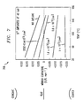
- FIGURE 7 represents the experimental data showing the effects of different Si + ion implantation doses on the temperature-dependence of mirror curvature.
- the implant dose is increased, the initially concave mirror curvature at room temperature is gradually opened up toward the flat mirror at a dose of about 1E16 ions/cm 2 , and then the trend of mirror opening up continues further into convex state at higher doses of implantation.
- a selection of proper implant dose can be utilized to conveniently fine tune and adjust the mirror curvature if the starting curvature is concave in nature.
- the temperature-dependence of mirror curvature i.e., the slope of the thermal cycling curves, is substantially reduced by implantation, with the degree of reduction increasing with increasing dose of implantation.
- the ion implanting may optionally be performed by blanket implantation on the whole or on a large area portion of the device surface, or may be performed only on selected areas (e.g., only where the light reflective optical layer 310 is present). This could be accomplished by patterned masking, depending on the convenience of fabrication processing.
- the ion implanted mirror array may be used as-implanted, or after being subjected to additional annealing heat treatment. For example, this could be done to facilitate the formation of precipitate particles in the light reflective optical layer 310 or to intentionally allow creep deformation so that time or temperature-dependent change of mirror curvature during service is minimized.
- the structure of atomic arrangement in the light reflective optical layer 310 and a surface portion of the mirror substrate 210 are altered by the implanted dopant 410.
- the implantation inserts foreign atoms into the lattice structure of the host material thus increasing the tensile stress in the light reflective optical layer 310, and the mirror substrate 210 if the implanting ions penetrate somewhat into the mirror substrate 210 as well. Induced tensile stress on the surface portion of the thin materials tends to correct the concave curvature of the mirror structure toward a desirably flat configuration.
- the process of doping the light reflective optical layer 310 may introduce, in addition to the implanted atoms or precipitate particles, other defects such as dislocations and point defects in the lattice structure of the light reflective optical layer 310, and mirror substrate 210 if included therein. Furthermore, the dopant strengthens the otherwise very soft light reflective optical layers 310 and reduces the undesirable time or temperature-dependent curvature change.
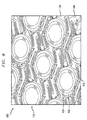
- FIGURE 8 illustrated is a photomicrograph showing an exemplary electro-optic device 800 comprising an array of mirrors 110.
- the device 800 was fabricated by MEMS micro machining process which involves multilayer deposition and selective etching.
- the mirror assembly 110 is raised above the mounting substrate 120 by using the upward bending of lift arms 810 during the release process for the MEMS structure.
- the mirrors 110 in this particular embodiment are double gimbal cantilevered and attached onto a frame structure 820 by springs 830, and hence can be tilted to any desired orientation for optical signal routing via electrostatic or other actuation with electrical voltage or current supplied from outside, e.g., through contact pads 840.
- the inventive mirror 110 illustrated in FIGURE 1 is dimensionally stabilized in terms of flatness by the ion implantation. Thus, the mirror 110 exhibits substantially reduced time- and temperature-dependent change of mirror curvature.
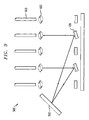
- the optical communications system 900 includes input/output fiber bundles 910, the micro-electro-mechanical structure 100 illustrated in FIGURE 1, an imaging lense 920 interposed between the input/output fiber bundles 910 and the micro-electro mechanical structure 100, and a reflector 930.
- the optical communications system 900 represents an optical cross-connect, which is one environment where the micro-electro-mechanical structure 100 may be used.
- the inventive micro-electro-mechanical system optical device 100 is useful not only for channel cross-connect, but also for signal re-routing, or signal modification in optical communication networking system.
- FIGURE 10 Schematically illustrated in FIGURE 10 is an example of such a communication system 1000 comprising an optical cross connect and other functional devices.
- each mirror receives a demultiplexed optical signal from an incoming channel, and reflect it toward an intended output channel location.
- the inventive device is also useful for various other light-reflecting mirror systems, since the stability of mirror curvature is essential for reliable operation of most of the MEMS based optical devices. Examples of such devices include those shown in FIGURE 10, such as power gain equalizers, switches, wavelength-division-multiplexer (WDM) add/drop devices, optical modulators and optical signal attenuators.
- WDM wavelength-division-multiplexer
- Multi-wavelength optical communication systems will require reconfiguration and reallocation of wavelengths among the various nodes of a network depending on user requirements, e.g., with programmable add/drop elements.
- One problem limiting the capacity of such systems is that the erbium-doped fiber amplifier, which is often a necessary component in optical communication systems, has a characteristic spectral dependence providing different gain for different wavelength channels. This spectral dependence poses a problem for multichannel WDM systems, because different gains for different channels leads to high bit error rates in some of the channels.
- the amplifier will start showing deleterious peaks in its gain spectrum at some wavelength channels, requiring modification of the signal spectrum and flattening of the amplifier gains.
- a long-period fiber grating device provides wavelength dependent loss and may be used for spectral shaping. See an article by A.M. Vengsarkar et al ., Optical Letters Vol.21, p.336, (1996).
- a long-period grating couples optical power between two co-propagating modes with very low back reflections.
- a long-period grating typically comprises a length of optical waveguide wherein a plurality of refractive index perturbations are spaced along the waveguide by a periodic distance, which is large compared to the wavelength of the transmitted light.
- Long-period fiber grating devices selectively remove light at specific wavelengths by mode conversion.
- a non-guided mode is a mode which is not confined to the core, but rather, is defined by the entire waveguide structure, e.g., based on a cladding mode.
- a difficulty with conventional long-period gratings is that their ability to dynamically equalize amplifier gain is limited, because they filter only a fixed wavelength acting as wavelength-dependent loss elements.
- Such dynamic gain equalizers based on reconfigurable long-period gratings have been disclosed, for example, in the US Patent No. 5999671 (Jin, et al .). It is desirable to be able to equalize amplifier gains over a broad range of wavelengths covering many wavelength channels. Therefore, it would be beneficial to utilize the micro-electro-mechanical system optical device 100, and design dynamic gain equalizer devices so that the range of wavelength spectrum and the number of wavelength channels simultaneously controllable can be increased.
- the optical signal gain in each wavelength channel can be independently, and simultaneously with other channels, controlled by the micro-electro-mechanical system optical device 100, which reflects that particular signal.
- the multiplexed optical is demultiplexed using suitable demultiplexers such as planar waveguides or thin film devices, with each of the separated wavelength channel signal being sent to each micro-electromechanical system optical device 100 and reflected.
- suitable demultiplexers such as planar waveguides or thin film devices
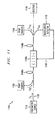
- the system 1100 comprises dynamically gain-equalized optical amplifiers, a reconfigurable MEMS minor-type spectral shaping device, and a feedback device.
- the system 1100 comprises a transmitter source 1110 of optical signals such as a digitally modulated 1.55 mm signal, an optical signal path comprising a length of optical fiber 1120 for transmitting the signal, and a receiver 113 0 for receiving and demodulating the signal.
- One or more optical amplifiers such as erbium-doped fiber amplifiers 1140a. 1140b, are disposed in the optical signal path for amplifying the transmitted signal.
- the amplifiers are pumped by pump sources 1150, 1160, of optical energy having pump wavelengths ⁇ p1 , and ⁇ p2 .
- One of the preferred uses of the device of FIGURE 11 is to reduce spectral dependence in the gain output of an optical amplifier.
- the characteristic gain spectrum of an erbium-doped optical fiber amplifier has a pair of gain peaks at about 1.53min and at about 1.56mm.
- a signal at 1.53mm will be amplified more than one at 1.54mm, which would be disadvantageous in a wavelength division multiplexing (WDM) system.
- WDM wavelength division multiplexing
- the tunable system 1180 comprises a demultiplexer in combination with a tunable light-reflecting MEMS mirror device and a multiplexer to put together the different wavelength channels into the optical fiber.
- the device 1180 is connected to a feedback system 1190, having a wavelength detector 1170 coupled to the fiber 1120 for detecting the wavelength response ⁇ p .
- the feedback system 1190 automatically adjusts the tuning of the device 1180 depending upon ⁇ tap .
- system 1100 can be a WDM system using a plurality of different wavelength signals, e.g. ⁇ S1 and ⁇ S2 , and a plurality of tunable MEMS mirror devices coupled to one or more detectors.
- the micro-electro-mechanical system optical device 100 can also be useful as a multi-channel optical add/drop device.
- Modern, high-density optical communications utilize wavelength division multiplexed communication systems which employ multiplexer/demultiplexer devices.
- a "trunk" fiber carries optical signal channels at several wavelengths ⁇ 1 , ⁇ 2 , ... ⁇ n and it is desirable to extract a single wavelength channel from the trunk fiber or to add a single wavelength channel onto the trunk.
- a wide variety of such devices can be made, for example, by interconnecting optical circulators and tunable fiber Bragg gratings. See, US Patent No. 5781677 by Jin et al .
- the channel reflected by the grating is dropped to the trunk fiber or is added to the trunk.
- Gratings as described herein permit selection at the grating of which channel is dropped or added.
- the micro-electro-mechanical system optical device 100 allows channel add/drop operation in a free-space mode thus providing a convenient capability to carry out the add/drop operations for many hundreds or even thousands of channels simultaneously.
- Filters and attenuators are useful in communication systems to change the power levels of various signals.
- variable attenuators are becoming increasingly more important, especially in dense wavelength-division multiplexed (DWDM) systems.
- DWDM dense wavelength-division multiplexed
- Variable attenuators are used to vary the amount of loss, light will experience as it passes through the system. This loss may range from low loss ( ⁇ 1dB), to very high loss (> 30dB).
- the mechanism by which the attenuators induce loss in the signals may be attributable to coupling loss between fibers, polarization loss, absorption loss, scattering loss, or any combination of these.
- Variable attenuators typically include complicated structures with moving parts that rotate or otherwise move the position of the fibers or a separate attenuator device.
- U.S. Pat. No. 5,745,634 to Garrett, et al., "Voltage Controlled Attenuator,” issued April 28, 1998 shows a variable attenuator with which the variation in attenuation is obtained by actuating a DC motor which displaces the position of the attenuator.
- U.S. Pat. No. 5,677,977 to Smith Optical Attenuator
- a variable attenuator based on coupling loss is typically composed of two separated fibers whose separation is controlled with mechanical motion. As the amount of the separation between the fibers increases, the amount of loss also increases. See, for example, Brenner et al., "Low-Reflectivity In-Line Variable Attenuator Utilizing Optical Fiber Tapers," J. LIGHTWAVE TECH., Vol. 18 (1990), at p. 7, and U.S. application Serial No. 09/097,549, “Magnetically Controlled Variable Optical Attenuators,” filed by Espindola et al. on June 15, 1998, and assigned to the present assignee, which is incorporated herein by reference.
- variable attenuators typically have involved use of bulk moving parts and are not always amenable to small, high-density device arrays.
- those concerned with the development of optical communications systems continually search for new components and designs including new attenuator designs.
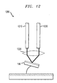
- the instant invention comprising a micro-electro-mechanical system optical device 100, such as schematically illustrated in FIGURE 12, provides a variable attenuator device that may be used to reliably achieve desired signal attenuation in many channels.
- a first fiber optic line 1210, a lense 1220, the micro-electro-mechanical system optical device 100 and a second offset fiber optic line 1230 are also included within the embodiment shown in FIGURE 12 .
- any light-reflecting system comprising a mirror or an array of mirrors with surface light reflecting metal film can be improved by the insertion of the implanted dopant.
- the mirror size may be larger than about 1 cm in diameter.
Landscapes
- Physics & Mathematics (AREA)
- Engineering & Computer Science (AREA)
- General Physics & Mathematics (AREA)
- Optics & Photonics (AREA)
- Microelectronics & Electronic Packaging (AREA)
- Mechanical Engineering (AREA)
- Manufacturing & Machinery (AREA)
- Mechanical Light Control Or Optical Switches (AREA)
- Micromachines (AREA)
- Optical Elements Other Than Lenses (AREA)
Abstract
Description
Claims (28)
- A micro-electro-mechanical system (MEMS) optical device, comprising:a mirror having a light reflective optical layer containing at least one type of an implanted dopant located over a substrate; anda mounting substrate on which the mirror is movably mounted.
- The micro-electro-mechanical system (MEMS) optical device recited in claim 1 further including an adhesion layer located between the substrate and the light reflective optical layer.
- The micro-electro-mechanical system (MEMS) optical device recited in claim 2 further including at least one type of dopant located within at least a portion of the adhesion layer and the substrate.
- The micro-electro-mechanical system (MEMS) optical device recited in claim 3 wherein the dopant located within at least a portion of the adhesion layer is present in a concentration of at least 1E14 atoms/cm3.
- The micro-electro-mechanical system (MEMS) optical device recited in any one of claims 1 to 4, wherein the dopant concentration in the light reflective optical layer is at least 1E15 atoms/cm3.
- The micro-electro-mechanical system (MEMS) optical device recited in any one of claims 1 to 5, wherein the at least one type of implanted dopant has a solid solubility in the light reflective optical layer that is less than 1 atomic percent.
- The micro-electro-mechanical system (MEMS) optical device recited in any one claims 1 to 6, wherein the light reflective optical layer comprises a material selected from the group consisting of gold, silver, rhodium, platinum, copper, aluminum or a combination thereof
- The micro-electro-mechanical system (MEMS) optical device recited in any one of claims 1 to 7, wherein the doped light reflective optical layer is doped with silicon and wherein the dopant concentration in the light reflective optical layer ranges from 1E15 atoms/cm3 to 1E22 atoms/cm3.
- The micro-electro-mechanical system (MEMS) optical device as recited in any one of claims 1 to 8, wherein the substrate comprises a material selected from the group consisting of polysilicon, single crystal silicon, silicon nitride, silicon carbide, silicon oxide, diamond film, or any regional and layered combination of these materials.
- The micro-electro-mechanical system (MEMS) optical device as recited in any one of claims 1 to 9, wherein at least one of the implanted dopants in the light reflective optical layer is in the form of clusters having a size ranging from about 1 nm to about 1000 nm.
- A method of manufacturing a micro-electro-mechanical system (MEMS) optical device, comprising:forming a mirror having a light reflective optical layer containing at least one type of an implanted dopant located over a substrate; andforming a mounting substrate on which the mirror is movably mounted.
- The method as recited in claim 11 further including forming an adhesion layer between the substrate and the light reflective optical layer.
- The method as recited in claim 12 further including implanting at least one type of dopant within at least a portion of the adhesion layer and the substrate.
- The method recited in claim 12 or 13 wherein implanting at least one type of dopant includes implanting at least one type of dopant within at least a portion of the adhesion layer and the substrate at a concentration of at least 1E14 atoms/cm3.
- The method recited in any one of claims 11 to 14, wherein the light reflective optical layer having at least one type of implanted dopant has a concentration of at least about 1E15 atoms/cm3.
- The method recited in any one of claims 11 to 15, wherein the mirror comprises a material selected from the group consisting of gold, silver, rhodium, platinum, copper, aluminum and a combination thereof
- The method recited in claim 16 wherein at least one type of an implanted dopant comprises silicon and the light reflective optical layer has a silicon dopant concentration ranging from 1E15 atoms/cm3 to 1E22 atoms/cm3.
- The method as recited in any one of claims 11 to 17, wherein the substrate is polysilicon.
- The method as recited in any one of claims 11 to 18 wherein forming a mirror having a dopant located therein that is in the form of clusters having a size ranging from about 1 nm to about 1000 nm includes subjecting the mirror to a heat treatment below 400°C.
- The method as recited in any one of claims 11 to 19, wherein forming a light reflective optical layer includes forming a light reflective optical layer using a process selected from the group consisting of evaporation, sputtering, electrochemical deposition, chemical vapor deposition, followed by an ion implantation doping process with one or more dopants.
- The method as recited in any one of claims 11 to 20, wherein forming a light reflective layer includes using an extraction voltage for doping the light reflective layer such that at least 60% of the implanted dopant gets trapped and retained in the light reflective layer, with the remaining dopant penetrating into the substrate.
- The method as recited in claim 21 wherein the extraction voltage is in the range from 2 KeV to 1000 KeV.
- The method as recited in any one of claims 11 to 22, wherein forming a mirror having at least one type of an implanted dopant includes subjecting the mirror to a shadow mask or lithographic patterning process.
- An optical communications system, comprising:input/output fiber bundles;a micro-electro-mechanical structure, comprising:a mirror having a light reflective optical layer containing at least one type of an implanted dopant located over a substrate; anda mounting substrate on which the mirror is movably mounted;imaging lenses interposed between the input/output fiber bundles and the micro-electro-mechanical structure; anda reflector.
- The optical communications system recited in claim 24 further including an adhesion layer located between the substrate and the light reflective optical layer.
- The optical communications system recited in claim 24 or 25, wherein the at least one type of dopant is present in the light reflective optical layer in a concentration of at least 1E15 atoms/cm3.
- The optical communications system recited in claim 24, 25 or 26, wherein the doped light reflective optical layer comprises a material selected from the group consisting of gold, silver, rhodium, platinum, copper, aluminum or a combination thereof.
- The optical communications system recited in any one of claims 24 to 27, that comprises one or more devices selected from the group consisting of:a micro-electro-mechanical system (MEMS) optical cross connect system;an optical power gain equalizer system;a wavelength division multiplexing telecommunications system;a light signal switch in an optical communications system; anda variable optical attenuator in an optical communications system.
Applications Claiming Priority (2)
| Application Number | Priority Date | Filing Date | Title |
|---|---|---|---|
| US09/685,883 US6522801B1 (en) | 2000-10-10 | 2000-10-10 | Micro-electro-optical mechanical device having an implanted dopant included therein and a method of manufacture therefor |
| US685883 | 2000-10-10 |
Publications (3)
| Publication Number | Publication Date |
|---|---|
| EP1197778A2 true EP1197778A2 (en) | 2002-04-17 |
| EP1197778A3 EP1197778A3 (en) | 2003-07-16 |
| EP1197778B1 EP1197778B1 (en) | 2006-03-29 |
Family
ID=24754062
Family Applications (1)
| Application Number | Title | Priority Date | Filing Date |
|---|---|---|---|
| EP01308610A Expired - Lifetime EP1197778B1 (en) | 2000-10-10 | 2001-10-09 | Micro-electro-optical mechanical device having an implanted dopant included therein and a method of manufacture therefor |
Country Status (4)
| Country | Link |
|---|---|
| US (1) | US6522801B1 (en) |
| EP (1) | EP1197778B1 (en) |
| JP (1) | JP2002196267A (en) |
| DE (1) | DE60124794T2 (en) |
Cited By (3)
| Publication number | Priority date | Publication date | Assignee | Title |
|---|---|---|---|---|
| WO2006036437A1 (en) * | 2004-09-27 | 2006-04-06 | Idc, Llc | Device and method for modifying actuation voltage thresholds of a deformable membrane in an interferometric modulator |
| US8659816B2 (en) | 2011-04-25 | 2014-02-25 | Qualcomm Mems Technologies, Inc. | Mechanical layer and methods of making the same |
| US8830557B2 (en) | 2007-05-11 | 2014-09-09 | Qualcomm Mems Technologies, Inc. | Methods of fabricating MEMS with spacers between plates and devices formed by same |
Families Citing this family (72)
| Publication number | Priority date | Publication date | Assignee | Title |
|---|---|---|---|---|
| US7550794B2 (en) * | 2002-09-20 | 2009-06-23 | Idc, Llc | Micromechanical systems device comprising a displaceable electrode and a charge-trapping layer |
| US7297471B1 (en) | 2003-04-15 | 2007-11-20 | Idc, Llc | Method for manufacturing an array of interferometric modulators |
| WO2003007049A1 (en) | 1999-10-05 | 2003-01-23 | Iridigm Display Corporation | Photonic mems and structures |
| US7071520B2 (en) * | 2000-08-23 | 2006-07-04 | Reflectivity, Inc | MEMS with flexible portions made of novel materials |
| US7057246B2 (en) * | 2000-08-23 | 2006-06-06 | Reflectivity, Inc | Transition metal dielectric alloy materials for MEMS |
| US6747845B1 (en) * | 2000-10-11 | 2004-06-08 | International Business Machines Corporation | Modified strain region of strain reactive slider with implanted ions, electrons or neutral atoms |
| US7057251B2 (en) * | 2001-07-20 | 2006-06-06 | Reflectivity, Inc | MEMS device made of transition metal-dielectric oxide materials |
| TW503330B (en) * | 2001-10-17 | 2002-09-21 | Hon Hai Prec Ind Co Ltd | Optical switch and method for alignment thereof |
| US6754431B2 (en) * | 2001-10-24 | 2004-06-22 | Intel Corporation | Variable optical attenuator |
| KR100421222B1 (en) * | 2001-11-24 | 2004-03-02 | 삼성전자주식회사 | Micro switching device actuated by low voltage |
| US6794119B2 (en) | 2002-02-12 | 2004-09-21 | Iridigm Display Corporation | Method for fabricating a structure for a microelectromechanical systems (MEMS) device |
| US6956983B2 (en) * | 2002-05-31 | 2005-10-18 | Intel Corporation | Epitaxial growth for waveguide tapering |
| US6989284B2 (en) * | 2002-05-31 | 2006-01-24 | Intel Corporation | Fabrication of a waveguide taper through ion implantation |
| US20030228089A1 (en) * | 2002-06-11 | 2003-12-11 | Scott Blackstone | Method of controlling the curvature of an optical device |
| US7208809B2 (en) * | 2002-09-19 | 2007-04-24 | Nippon Telegraph And Telephone Corporation | Semiconductor device having MEMS |
| US7781850B2 (en) * | 2002-09-20 | 2010-08-24 | Qualcomm Mems Technologies, Inc. | Controlling electromechanical behavior of structures within a microelectromechanical systems device |
| US6778315B2 (en) * | 2002-09-25 | 2004-08-17 | Rosemount Aerospace Inc. | Micro mirror structure with flat reflective coating |
| TW594360B (en) | 2003-04-21 | 2004-06-21 | Prime View Int Corp Ltd | A method for fabricating an interference display cell |
| TW570896B (en) * | 2003-05-26 | 2004-01-11 | Prime View Int Co Ltd | A method for fabricating an interference display cell |
| US7221495B2 (en) * | 2003-06-24 | 2007-05-22 | Idc Llc | Thin film precursor stack for MEMS manufacturing |
| TWI231865B (en) * | 2003-08-26 | 2005-05-01 | Prime View Int Co Ltd | An interference display cell and fabrication method thereof |
| TWI232333B (en) * | 2003-09-03 | 2005-05-11 | Prime View Int Co Ltd | Display unit using interferometric modulation and manufacturing method thereof |
| TW593126B (en) * | 2003-09-30 | 2004-06-21 | Prime View Int Co Ltd | A structure of a micro electro mechanical system and manufacturing the same |
| US7459325B2 (en) * | 2004-01-05 | 2008-12-02 | Texas Instruments Incorporated | MEMS passivation with transition metals |
| US20050162765A1 (en) * | 2004-01-22 | 2005-07-28 | Hagelin Paul M. | Micromirror with rib reinforcement |
| SG118264A1 (en) * | 2004-06-29 | 2006-01-27 | Sony Corp | A magnetic material and a MEMS device using the magnetic material |
| US7349136B2 (en) * | 2004-09-27 | 2008-03-25 | Idc, Llc | Method and device for a display having transparent components integrated therein |
| US20060067650A1 (en) * | 2004-09-27 | 2006-03-30 | Clarence Chui | Method of making a reflective display device using thin film transistor production techniques |
| US7429334B2 (en) * | 2004-09-27 | 2008-09-30 | Idc, Llc | Methods of fabricating interferometric modulators by selectively removing a material |
| US7417783B2 (en) * | 2004-09-27 | 2008-08-26 | Idc, Llc | Mirror and mirror layer for optical modulator and method |
| US7553684B2 (en) * | 2004-09-27 | 2009-06-30 | Idc, Llc | Method of fabricating interferometric devices using lift-off processing techniques |
| US7492502B2 (en) * | 2004-09-27 | 2009-02-17 | Idc, Llc | Method of fabricating a free-standing microstructure |
| US20060065622A1 (en) * | 2004-09-27 | 2006-03-30 | Floyd Philip D | Method and system for xenon fluoride etching with enhanced efficiency |
| US7373026B2 (en) * | 2004-09-27 | 2008-05-13 | Idc, Llc | MEMS device fabricated on a pre-patterned substrate |
| US7684104B2 (en) | 2004-09-27 | 2010-03-23 | Idc, Llc | MEMS using filler material and method |
| US7161730B2 (en) * | 2004-09-27 | 2007-01-09 | Idc, Llc | System and method for providing thermal compensation for an interferometric modulator display |
| US7405861B2 (en) * | 2004-09-27 | 2008-07-29 | Idc, Llc | Method and device for protecting interferometric modulators from electrostatic discharge |
| US20060065366A1 (en) * | 2004-09-27 | 2006-03-30 | Cummings William J | Portable etch chamber |
| US20060066932A1 (en) * | 2004-09-27 | 2006-03-30 | Clarence Chui | Method of selective etching using etch stop layer |
| TW200628877A (en) * | 2005-02-04 | 2006-08-16 | Prime View Int Co Ltd | Method of manufacturing optical interference type color display |
| JP2009503564A (en) * | 2005-07-22 | 2009-01-29 | クアルコム,インコーポレイテッド | Support structure for MEMS device and method thereof |
| BRPI0612997A2 (en) | 2005-07-22 | 2010-12-14 | Qualcomm Incorporated | MEM devices and their manufacturing methods |
| EP2495212A3 (en) | 2005-07-22 | 2012-10-31 | QUALCOMM MEMS Technologies, Inc. | Mems devices having support structures and methods of fabricating the same |
| US7630114B2 (en) * | 2005-10-28 | 2009-12-08 | Idc, Llc | Diffusion barrier layer for MEMS devices |
| US7795061B2 (en) * | 2005-12-29 | 2010-09-14 | Qualcomm Mems Technologies, Inc. | Method of creating MEMS device cavities by a non-etching process |
| US7382515B2 (en) * | 2006-01-18 | 2008-06-03 | Qualcomm Mems Technologies, Inc. | Silicon-rich silicon nitrides as etch stops in MEMS manufacture |
| US7547568B2 (en) * | 2006-02-22 | 2009-06-16 | Qualcomm Mems Technologies, Inc. | Electrical conditioning of MEMS device and insulating layer thereof |
| US7450295B2 (en) * | 2006-03-02 | 2008-11-11 | Qualcomm Mems Technologies, Inc. | Methods for producing MEMS with protective coatings using multi-component sacrificial layers |
| US20070228156A1 (en) * | 2006-03-28 | 2007-10-04 | Household Corporation | Interoperability facilitator |
| US7643203B2 (en) * | 2006-04-10 | 2010-01-05 | Qualcomm Mems Technologies, Inc. | Interferometric optical display system with broadband characteristics |
| US7574096B2 (en) * | 2006-04-10 | 2009-08-11 | Lightconnect, Inc. | Optical attenuator |
| US7527996B2 (en) | 2006-04-19 | 2009-05-05 | Qualcomm Mems Technologies, Inc. | Non-planar surface structures and process for microelectromechanical systems |
| US7711239B2 (en) * | 2006-04-19 | 2010-05-04 | Qualcomm Mems Technologies, Inc. | Microelectromechanical device and method utilizing nanoparticles |
| US7623287B2 (en) * | 2006-04-19 | 2009-11-24 | Qualcomm Mems Technologies, Inc. | Non-planar surface structures and process for microelectromechanical systems |
| US7417784B2 (en) * | 2006-04-19 | 2008-08-26 | Qualcomm Mems Technologies, Inc. | Microelectromechanical device and method utilizing a porous surface |
| US20070249078A1 (en) * | 2006-04-19 | 2007-10-25 | Ming-Hau Tung | Non-planar surface structures and process for microelectromechanical systems |
| US7369292B2 (en) * | 2006-05-03 | 2008-05-06 | Qualcomm Mems Technologies, Inc. | Electrode and interconnect materials for MEMS devices |
| US7405863B2 (en) * | 2006-06-01 | 2008-07-29 | Qualcomm Mems Technologies, Inc. | Patterning of mechanical layer in MEMS to reduce stresses at supports |
| US7321457B2 (en) * | 2006-06-01 | 2008-01-22 | Qualcomm Incorporated | Process and structure for fabrication of MEMS device having isolated edge posts |
| US7566664B2 (en) * | 2006-08-02 | 2009-07-28 | Qualcomm Mems Technologies, Inc. | Selective etching of MEMS using gaseous halides and reactive co-etchants |
| US7763546B2 (en) | 2006-08-02 | 2010-07-27 | Qualcomm Mems Technologies, Inc. | Methods for reducing surface charges during the manufacture of microelectromechanical systems devices |
| US7545552B2 (en) * | 2006-10-19 | 2009-06-09 | Qualcomm Mems Technologies, Inc. | Sacrificial spacer process and resultant structure for MEMS support structure |
| US7706042B2 (en) | 2006-12-20 | 2010-04-27 | Qualcomm Mems Technologies, Inc. | MEMS device and interconnects for same |
| US7535621B2 (en) | 2006-12-27 | 2009-05-19 | Qualcomm Mems Technologies, Inc. | Aluminum fluoride films for microelectromechanical system applications |
| US7625825B2 (en) * | 2007-06-14 | 2009-12-01 | Qualcomm Mems Technologies, Inc. | Method of patterning mechanical layer for MEMS structures |
| US8068268B2 (en) * | 2007-07-03 | 2011-11-29 | Qualcomm Mems Technologies, Inc. | MEMS devices having improved uniformity and methods for making them |
| US7863079B2 (en) | 2008-02-05 | 2011-01-04 | Qualcomm Mems Technologies, Inc. | Methods of reducing CD loss in a microelectromechanical device |
| JP5682165B2 (en) * | 2010-07-23 | 2015-03-11 | セイコーエプソン株式会社 | Interference filter, optical module, and analyzer |
| US8648959B2 (en) | 2010-11-11 | 2014-02-11 | DigitalOptics Corporation Europe Limited | Rapid auto-focus using classifier chains, MEMS and/or multiple object focusing |
| US11199665B2 (en) * | 2020-01-28 | 2021-12-14 | Hewlett Packard Enterprise Development Lp | Optical device for redirecting optical signals |
| EP3865453A1 (en) * | 2020-02-13 | 2021-08-18 | Miraex SA | Micro-opto-mechanical system sensor, arrangement and manufacturing method |
| JP7680203B2 (en) | 2020-12-21 | 2025-05-20 | 浜松ホトニクス株式会社 | Manufacturing method of mirror device |
Family Cites Families (8)
| Publication number | Priority date | Publication date | Assignee | Title |
|---|---|---|---|---|
| US5661591A (en) * | 1995-09-29 | 1997-08-26 | Texas Instruments Incorporated | Optical switch having an analog beam for steering light |
| US5867297A (en) * | 1997-02-07 | 1999-02-02 | The Regents Of The University Of California | Apparatus and method for optical scanning with an oscillatory microelectromechanical system |
| US6300619B1 (en) * | 1997-12-22 | 2001-10-09 | Lucent Technologies Inc. | Micro-electro-mechanical optical device |
| US6392221B1 (en) * | 1997-12-22 | 2002-05-21 | Agere Systems Guardian Corp. | Micro-electro-mechanical optical device |
| US6256430B1 (en) * | 1998-11-23 | 2001-07-03 | Agere Systems Inc. | Optical crossconnect system comprising reconfigurable light-reflecting devices |
| US6278812B1 (en) * | 1998-12-14 | 2001-08-21 | At&T Corporation | Protection schemes for mirror-failure in free-space micromachined optical switches |
| US6292600B1 (en) * | 1999-06-07 | 2001-09-18 | At&T Corp. | Angular-precision enhancement in free-space micromachined optical switches |
| US6288821B1 (en) * | 1999-10-01 | 2001-09-11 | Lucent Technologies, Inc. | Hybrid electro-optic device with combined mirror arrays |
-
2000
- 2000-10-10 US US09/685,883 patent/US6522801B1/en not_active Expired - Lifetime
-
2001
- 2001-10-09 DE DE60124794T patent/DE60124794T2/en not_active Expired - Lifetime
- 2001-10-09 EP EP01308610A patent/EP1197778B1/en not_active Expired - Lifetime
- 2001-10-10 JP JP2001312072A patent/JP2002196267A/en active Pending
Cited By (4)
| Publication number | Priority date | Publication date | Assignee | Title |
|---|---|---|---|---|
| WO2006036437A1 (en) * | 2004-09-27 | 2006-04-06 | Idc, Llc | Device and method for modifying actuation voltage thresholds of a deformable membrane in an interferometric modulator |
| EP2290426A1 (en) * | 2004-09-27 | 2011-03-02 | QUALCOMM MEMS Technologies, Inc. | Device and method for modifying actuation voltage thresholds of a deformable membrane in an interferometric modulator |
| US8830557B2 (en) | 2007-05-11 | 2014-09-09 | Qualcomm Mems Technologies, Inc. | Methods of fabricating MEMS with spacers between plates and devices formed by same |
| US8659816B2 (en) | 2011-04-25 | 2014-02-25 | Qualcomm Mems Technologies, Inc. | Mechanical layer and methods of making the same |
Also Published As
| Publication number | Publication date |
|---|---|
| EP1197778B1 (en) | 2006-03-29 |
| US6522801B1 (en) | 2003-02-18 |
| DE60124794D1 (en) | 2007-01-04 |
| JP2002196267A (en) | 2002-07-12 |
| DE60124794T2 (en) | 2007-03-01 |
| EP1197778A3 (en) | 2003-07-16 |
Similar Documents
| Publication | Publication Date | Title |
|---|---|---|
| EP1197778B1 (en) | Micro-electro-optical mechanical device having an implanted dopant included therein and a method of manufacture therefor | |
| US6639724B2 (en) | Device having a barrier layer located therein and a method of manufacture therefor | |
| US6704475B2 (en) | Mirror for use with a micro-electro-mechanical system (MEMS) optical device and a method of manufacture therefor | |
| US6618184B2 (en) | Device for use with a micro-electro-mechanical system (MEMS) optical device and a method of manufacture therefor | |
| US6915046B2 (en) | Optical systems comprising curved MEMs mirrors and methods for making same | |
| US7015056B2 (en) | Electro-mechanical device having a charge dissipation layer and a method of manufacture therefor | |
| US6574026B2 (en) | Magnetically-packaged optical MEMs device | |
| US7304799B2 (en) | Tunable optical filter with heater on a CTE-matched transparent substrate | |
| Day et al. | Tapered silicon waveguides for low insertion loss highly-efficient high-speed electronic variable optical attenuators | |
| US6711317B2 (en) | Resiliently packaged MEMs device and method for making same | |
| EP1743201A1 (en) | Athermal awg and awg with low power consumption using groove of changeable width | |
| US7539364B2 (en) | Method and apparatus facilitating mechanical beam steering for optical integrated circuits | |
| US6730615B2 (en) | High reflector tunable stress coating, such as for a MEMS mirror | |
| US6907181B2 (en) | Variable optical attenuator | |
| US7052733B2 (en) | Method for making thin film filter having a negative temperature drift coefficient | |
| US7268927B2 (en) | Tunable optical filter array and method of use | |
| JP2005266005A (en) | Optical circuit with photonic crystal and manufacturing method therefor | |
| US7106487B2 (en) | Thermal tuning of a laser using doped silicon etalon | |
| Lin | Micro-Electro-Mechanical Systems (MEMS) for Optical-Fiber Communications |
Legal Events
| Date | Code | Title | Description |
|---|---|---|---|
| PUAI | Public reference made under article 153(3) epc to a published international application that has entered the european phase |
Free format text: ORIGINAL CODE: 0009012 |
|
| AK | Designated contracting states |
Kind code of ref document: A2 Designated state(s): AT BE CH CY DE DK ES FI FR GB GR IE IT LI LU MC NL PT SE TR |
|
| AX | Request for extension of the european patent |
Free format text: AL;LT;LV;MK;RO;SI |
|
| RIN1 | Information on inventor provided before grant (corrected) |
Inventor name: AKSYUK, VLADIMIR A. Inventor name: PARDO, FLAVIO Inventor name: JIN, SUNGHO Inventor name: KIM, JUNGSANG Inventor name: MAVOORI, HAREESH Inventor name: RAMIREZ, AINISSA |
|
| PUAL | Search report despatched |
Free format text: ORIGINAL CODE: 0009013 |
|
| AK | Designated contracting states |
Designated state(s): AT BE CH CY DE DK ES FI FR GB GR IE IT LI LU MC NL PT SE TR |
|
| AX | Request for extension of the european patent |
Extension state: AL LT LV MK RO SI |
|
| AKX | Designation fees paid | ||
| 17P | Request for examination filed |
Effective date: 20031118 |
|
| RBV | Designated contracting states (corrected) |
Designated state(s): DE FR GB |
|
| 17Q | First examination report despatched |
Effective date: 20040316 |
|
| REG | Reference to a national code |
Ref country code: DE Ref legal event code: 8566 |
|
| GRAP | Despatch of communication of intention to grant a patent |
Free format text: ORIGINAL CODE: EPIDOSNIGR1 |
|
| GRAS | Grant fee paid |
Free format text: ORIGINAL CODE: EPIDOSNIGR3 |
|
| GRAA | (expected) grant |
Free format text: ORIGINAL CODE: 0009210 |
|
| AK | Designated contracting states |
Kind code of ref document: B1 Designated state(s): DE FR GB |
|
| REG | Reference to a national code |
Ref country code: GB Ref legal event code: FG4D |
|
| ET | Fr: translation filed | ||
| REF | Corresponds to: |
Ref document number: 60124794 Country of ref document: DE Date of ref document: 20070104 Kind code of ref document: P |
|
| PLBE | No opposition filed within time limit |
Free format text: ORIGINAL CODE: 0009261 |
|
| STAA | Information on the status of an ep patent application or granted ep patent |
Free format text: STATUS: NO OPPOSITION FILED WITHIN TIME LIMIT |
|
| 26N | No opposition filed |
Effective date: 20070102 |
|
| REG | Reference to a national code |
Ref country code: FR Ref legal event code: PLFP Year of fee payment: 15 |
|
| REG | Reference to a national code |
Ref country code: FR Ref legal event code: PLFP Year of fee payment: 16 |
|
| REG | Reference to a national code |
Ref country code: FR Ref legal event code: PLFP Year of fee payment: 17 |
|
| PGFP | Annual fee paid to national office [announced via postgrant information from national office to epo] |
Ref country code: FR Payment date: 20170921 Year of fee payment: 17 Ref country code: GB Payment date: 20170925 Year of fee payment: 17 |
|
| PGFP | Annual fee paid to national office [announced via postgrant information from national office to epo] |
Ref country code: DE Payment date: 20170920 Year of fee payment: 17 |
|
| REG | Reference to a national code |
Ref country code: DE Ref legal event code: R119 Ref document number: 60124794 Country of ref document: DE |
|
| GBPC | Gb: european patent ceased through non-payment of renewal fee |
Effective date: 20181009 |
|
| PG25 | Lapsed in a contracting state [announced via postgrant information from national office to epo] |
Ref country code: DE Free format text: LAPSE BECAUSE OF NON-PAYMENT OF DUE FEES Effective date: 20190501 |
|
| PG25 | Lapsed in a contracting state [announced via postgrant information from national office to epo] |
Ref country code: FR Free format text: LAPSE BECAUSE OF NON-PAYMENT OF DUE FEES Effective date: 20181031 |
|
| PG25 | Lapsed in a contracting state [announced via postgrant information from national office to epo] |
Ref country code: GB Free format text: LAPSE BECAUSE OF NON-PAYMENT OF DUE FEES Effective date: 20181009 |