EP1195881A2 - Schaltnetzteil mit einer Einrichtung zur Funkstörspannungskompensation - Google Patents
Schaltnetzteil mit einer Einrichtung zur Funkstörspannungskompensation Download PDFInfo
- Publication number
- EP1195881A2 EP1195881A2 EP01122337A EP01122337A EP1195881A2 EP 1195881 A2 EP1195881 A2 EP 1195881A2 EP 01122337 A EP01122337 A EP 01122337A EP 01122337 A EP01122337 A EP 01122337A EP 1195881 A2 EP1195881 A2 EP 1195881A2
- Authority
- EP
- European Patent Office
- Prior art keywords
- voltage
- power supply
- capacitor
- interference
- switched
- Prior art date
- Legal status (The legal status is an assumption and is not a legal conclusion. Google has not performed a legal analysis and makes no representation as to the accuracy of the status listed.)
- Withdrawn
Links
- 230000005855 radiation Effects 0.000 title 1
- 239000003990 capacitor Substances 0.000 claims abstract description 41
- 230000001629 suppression Effects 0.000 claims abstract description 11
- 239000004020 conductor Substances 0.000 claims abstract description 9
- 238000004804 winding Methods 0.000 claims abstract description 9
- 230000003071 parasitic effect Effects 0.000 claims abstract description 8
- 230000008878 coupling Effects 0.000 claims abstract 2
- 238000010168 coupling process Methods 0.000 claims abstract 2
- 238000005859 coupling reaction Methods 0.000 claims abstract 2
- 230000007935 neutral effect Effects 0.000 description 4
- 230000033228 biological regulation Effects 0.000 description 3
- 239000000523 sample Substances 0.000 description 3
- 238000013016 damping Methods 0.000 description 2
- 238000009499 grossing Methods 0.000 description 2
- 230000000694 effects Effects 0.000 description 1
- 238000004519 manufacturing process Methods 0.000 description 1
- 238000005259 measurement Methods 0.000 description 1
- 230000001681 protective effect Effects 0.000 description 1
- 230000001105 regulatory effect Effects 0.000 description 1
Images


Classifications
-
- H—ELECTRICITY
- H02—GENERATION; CONVERSION OR DISTRIBUTION OF ELECTRIC POWER
- H02M—APPARATUS FOR CONVERSION BETWEEN AC AND AC, BETWEEN AC AND DC, OR BETWEEN DC AND DC, AND FOR USE WITH MAINS OR SIMILAR POWER SUPPLY SYSTEMS; CONVERSION OF DC OR AC INPUT POWER INTO SURGE OUTPUT POWER; CONTROL OR REGULATION THEREOF
- H02M3/00—Conversion of DC power input into DC power output
- H02M3/22—Conversion of DC power input into DC power output with intermediate conversion into AC
- H02M3/24—Conversion of DC power input into DC power output with intermediate conversion into AC by static converters
- H02M3/28—Conversion of DC power input into DC power output with intermediate conversion into AC by static converters using discharge tubes with control electrode or semiconductor devices with control electrode to produce the intermediate AC
- H02M3/325—Conversion of DC power input into DC power output with intermediate conversion into AC by static converters using discharge tubes with control electrode or semiconductor devices with control electrode to produce the intermediate AC using devices of a triode or a transistor type requiring continuous application of a control signal
- H02M3/335—Conversion of DC power input into DC power output with intermediate conversion into AC by static converters using discharge tubes with control electrode or semiconductor devices with control electrode to produce the intermediate AC using devices of a triode or a transistor type requiring continuous application of a control signal using semiconductor devices only
- H02M3/33507—Conversion of DC power input into DC power output with intermediate conversion into AC by static converters using discharge tubes with control electrode or semiconductor devices with control electrode to produce the intermediate AC using devices of a triode or a transistor type requiring continuous application of a control signal using semiconductor devices only with automatic control of the output voltage or current, e.g. flyback converters
-
- H—ELECTRICITY
- H02—GENERATION; CONVERSION OR DISTRIBUTION OF ELECTRIC POWER
- H02M—APPARATUS FOR CONVERSION BETWEEN AC AND AC, BETWEEN AC AND DC, OR BETWEEN DC AND DC, AND FOR USE WITH MAINS OR SIMILAR POWER SUPPLY SYSTEMS; CONVERSION OF DC OR AC INPUT POWER INTO SURGE OUTPUT POWER; CONTROL OR REGULATION THEREOF
- H02M1/00—Details of apparatus for conversion
- H02M1/44—Circuits or arrangements for compensating for electromagnetic interference in converters or inverters
Definitions
- the invention relates to a switching power supply with a device for damping high-frequency interference voltages.
- the switched mode power supply is suitable for use in mains-operated electronic devices, in particular for devices that have a Power supply of low power (typically ⁇ 50 W) and with an output side Require safety extra-low voltage (SELV).
- SMPS switched mode power supply
- SELV output side Require safety extra-low voltage
- EN 55014 General devices
- EN 55015 lamps and accessories
- EN 55022 Section 5.1.3 "Probe” is the measurement with a probe on all connections, that are not network connections.
- FIG. 4 A circuit of a switched-mode power supply unit with a safety extra-low voltage on the output side, which is customary in the prior art, is shown in FIG. 4.
- This contains a transformer TR designed as a high-frequency transformer with a primary winding W1 and a secondary winding W2.
- Such a transformer TR also referred to as an electronic transformer, has a parasitic capacitance C par between the windings W1, W2.
- a series resistor R1 On the primary side are a series resistor R1, a first rectifier diode D1 and a first smoothing capacitor for rectifying an AC line voltage L, N, and an electronic switch T1 for switching the through the primary winding W1 flowing current with a switching frequency of typically 60 kHz to 120 kHz.
- the parasitic capacitance C par of the order of 10 -12 F between the windings W1, W2 of the transformer TR causes high-frequency switching signals to reach the secondary side from the primary side, that is to say the network side.
- all potentials on the secondary side — with respect to the neutral conductor N, which is generally coupled to protective earth, are superimposed with a high-frequency interference.
- a radio interference suppression capacitor C2 is connected between the neutral conductor N on the primary side and the secondary-side ground (0 V). In accordance with the aforementioned safety regulations, this capacitor C2 must be implemented by means of a Y1 capacitor or two Y2 capacitors connected in series.
- the capacitance of the capacitor C2 which is limited to a few nanofarads, allows however, generally reduce the interference signal to only a few 100 mV, which is the case with a Device version with terminals on the output voltage side but not sufficient to comply with the radio interference voltage values according to EN 60669 is.
- the invention is therefore based on the object of a switching power supply with improved Specify damping of interference voltages.
- the radio interference suppression capacitor is accordingly not on the secondary side - as is customary in the prior art - directly with the output voltage (usually to ground), but to an RF auxiliary voltage source connected to that transmitted by the parasitic capacitance Noise level compensated.
- the output voltage usually to ground
- an RF auxiliary voltage source connected to that transmitted by the parasitic capacitance Noise level compensated.
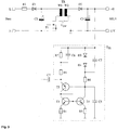
- Fig. 1 shows a representation of the circuit principle that the radio interference suppression capacitor C2 in an otherwise identical with Fig. 4 circuit on the secondary side not with the output voltage, but with an auxiliary RF voltage source Q Hi , which disturbs the parasitic capacitance C par transmitted interference voltage U. compensated, connected.
- the compensation voltage U comp generated by the auxiliary voltage source Q Hi must be identical to the interference signal U disturbance which arises between the ground (0 V) and the neutral conductor N.
- the parasitic capacitance C par of the transformer TR is, however, subject to large production variations, so that it can only be partially compensated for with a permanently set auxiliary voltage source Q Hi .
- the first embodiment variant of a circuit with an active regulation shown in FIG. 2 is better.
- the interference voltage U interference between neutral conductor N and ground (0 V) is measured via a measuring capacitor C2a, fed to an inverting amplifier, and compensated by means of a compensation capacitor C2b.
- the inverting amplifier is formed by a transistor T2, a base series resistor R2 and a collector resistor R3.
- the circuit with active regulation ensures a good compensation of the interference voltage; however, the two capacitors C2a and C2b must each be designed as a Y1 capacitor.
- an additional capacitor C4 can be connected between the output A TR of the transformer TR and the output A V of the amplifier (T2, R2, R3), as shown in FIG. 2, and should be dimensioned as follows: C 4 ⁇ W 1 W 2 C par . assuming that C4 is significantly smaller than C2b.
- the winding ratio was W1 / W2 ⁇ 30, the parasitic capacitance Cpar ⁇ 1 pF. This made it possible to reduce the radio interference voltage U Stör in the examined switching power supply by more than 20 dB compared to the standard implementation according to FIG. 4.
- a second circuit variant shown in FIG. 3 can be used.
- the auxiliary voltage source Q Hi is formed by the circuit part outlined with a dashed line in FIG. 3.
- the radio interference suppression capacitor C2 which is designed as a Y1 capacitor
- the auxiliary voltage source Q Hi which is connected to the output + U.
- the voltage drop across the radio interference suppression capacitor C2 is simulated with the aid of a standard capacitor of the same capacitance, namely a reference capacitor C5 of the auxiliary voltage source Q Hi .
- the auxiliary voltage source Q Hi also contains an emitter follower T5 and a circuit part formed by transistors T3 and T4 and associated emitter resistors R4 or R5, which is known as a current mirror. Resistors R6, R7 and R8 and diodes D3, D4 are arranged for setting the operating point or quiescent current. There are also RF block capacitors C6 and C7.
- this second circuit variant can (Fig.3) the interference level attenuation of the first variant (Fig .2) cannot be fully achieved; however, it is significantly better than a passive voltage divider and less expensive feasible as the first circuit variant.
- the components R7, D3 and D4 are used to set the operating point and are for the RF signal has no effect.
Landscapes
- Engineering & Computer Science (AREA)
- Power Engineering (AREA)
- Dc-Dc Converters (AREA)
Abstract
Description
- Fig. 1
- die Prinzipschaltung eines Schaltnetzteils mit erfindungsgemäßer Funkstörspannungskompensation,
- Fig. 2
- eine erste Schaltungsvariante zur Realisierung des Schaltnetzteils,
- Fig. 3
- eine zweite Schaltungsvariante zur Realisierung des Schaltnetzteils, und
- Fig. 4
- eine Prinzipschaltung eines Schaltnetzteils nach dem Stand der Technik.
Claims (4)
- Schaltnetzteil mit einem Transformator (TR) zur Kopplung eines Primärteils mit einem Sekundärteil, wobei der Primärteil dafür eingerichtet ist, eine hochfrequente Spannung zu erzeugen, und der Sekundärteil dafür eingerichtet ist, eine Ausgangs-Gleichspannung zu erzeugen, und wobei eine Einrichtung zur Kompensation einer hochfrequenten Störspannung (Ustör) vorhanden ist, die aufgrund einer zwischen Wicklungen (W1, W2) des Transformators (TR) bestehenden parasitären Kapazität (Cpar) im Schaltnetzteilbetrieb übertragen wird, dadurch gekennzeichnet, daßa) eine Reihenschaltung eines Funkentstörkondensators (C2) und einer Hilfsspannungsquelle (QHi) angeordnet ist, wobei die Hilfsspannungsquelle (QHi) dafür eingerichtet ist, eine Kompensationsspannung (Ucomp) zur Kompensation der Störspannung (Ustör) zu bilden, undb) diese Reihenschaltung (C2, QHi) als Verbindung eines Leiters (N) des Primärteils mit einem Leiter (0 V oder +U) des Sekundärteils angeordnet ist.
- Schaltnetzteil nach Anspruch 1, dadurch gekennzeichnet, daß die Hilfsspannungsquelle (QHi) durch einen invertierenden Verstärker (T2, R2, R3) gebildet ist, dem die mittels einem Meßkondensator (C2a) erfaßte Störspannung (Ustör) zugeführt ist, und als Funkentstörkondensator (C2) ein Kompensationskondensator (C2b) zwischen den Leiter (N) des Primärteils und den Ausgang (Av) des Verstärkers (T2, R2, R3) geschaltet ist.
- Schaltnetzteil nach Anspruch 2, dadurch gekennzeichnet, daß zur Kompensation sehr hoher Frequenzanteile ein zusätzlicher Kondensator (C4) zwischen den Ausgang (ATR) des Transformators (TR) und den Ausgang (Av) des Verstärkers (T2, R2, R3) geschaltet ist.
- Schaltnetzteil nach Anspruch 1, dadurch gekennzeichnet, daß die Hilfsspannungsquelle (QHi) durch eine Kompensationsspannungsquelle (K) gebildet ist, die einen Referenzkondensator (C5) und einen Stromspiegel (T3, T4) enthält, womit der Strom durch den Funkentstörkondensator (C2) über den Stromspiegel (T3, T4) in den Referenzkondensator (C5) gespiegelt wird.
Applications Claiming Priority (2)
| Application Number | Priority Date | Filing Date | Title |
|---|---|---|---|
| DE10048094A DE10048094B4 (de) | 2000-09-28 | 2000-09-28 | Schaltnetzteil mit einer Einrichtung zur Funkstörspannungskompensation |
| DE10048094 | 2000-09-28 |
Publications (2)
| Publication Number | Publication Date |
|---|---|
| EP1195881A2 true EP1195881A2 (de) | 2002-04-10 |
| EP1195881A3 EP1195881A3 (de) | 2004-01-21 |
Family
ID=7657973
Family Applications (1)
| Application Number | Title | Priority Date | Filing Date |
|---|---|---|---|
| EP01122337A Withdrawn EP1195881A3 (de) | 2000-09-28 | 2001-09-19 | Schaltnetzteil mit einer Einrichtung zur Funkstörspannungskompensation |
Country Status (2)
| Country | Link |
|---|---|
| EP (1) | EP1195881A3 (de) |
| DE (1) | DE10048094B4 (de) |
Cited By (2)
| Publication number | Priority date | Publication date | Assignee | Title |
|---|---|---|---|---|
| US6680463B2 (en) * | 2001-06-01 | 2004-01-20 | Sharp Kabushiki Kaisha | Power supply control circuit and cooking device |
| AT15424U1 (de) * | 2014-04-30 | 2017-08-15 | Tridonic Gmbh & Co Kg | Betriebsgerät, Leuchte und Verfahren zur Kommunikation über eine Potenzialbarriere |
Families Citing this family (1)
| Publication number | Priority date | Publication date | Assignee | Title |
|---|---|---|---|---|
| DE102019207182A1 (de) * | 2019-05-16 | 2020-11-19 | Osram Gmbh | Led-treiber mit sicherheitskleinspannung und mittel zur verhinderung von glimm-effekten |
Family Cites Families (9)
| Publication number | Priority date | Publication date | Assignee | Title |
|---|---|---|---|---|
| FR1585909A (de) * | 1968-05-15 | 1970-02-06 | ||
| DE1939652A1 (de) * | 1969-08-05 | 1971-02-11 | Kolbe & Co Hans | Siebschaltung zum Aussieben einer einem Gleichstrom ueberlagerten Stoerwechselspannung |
| JPS59129571A (ja) * | 1983-01-14 | 1984-07-25 | Tdk Corp | スイツチング電源 |
| DE3813584A1 (de) * | 1988-04-22 | 1989-11-02 | Blaupunkt Werke Gmbh | Schaltungsanordnung zur kompensation von stoerungen |
| SE512660C2 (sv) * | 1991-05-02 | 2000-04-17 | Ericsson Telefon Ab L M | Anläggning med radioutrustning innefattande en balanseringskrets för en störström |
| JPH08294275A (ja) * | 1995-04-21 | 1996-11-05 | Canon Inc | スイッチング電源 |
| US5724236A (en) * | 1996-03-05 | 1998-03-03 | Motorola, Inc. | Power converter transformer having an auxilliary winding and electrostatic shield to suppress noise |
| DE19741430A1 (de) * | 1997-09-19 | 1999-04-01 | Siemens Ag | Schaltungsanordnung und Verfahren zur Unterdrückung störender Rückwirkungen eines Umrichters |
| GB9812138D0 (en) * | 1998-06-06 | 1998-08-05 | Linn Prod Ltd | Noise suppression system for a power supply |
-
2000
- 2000-09-28 DE DE10048094A patent/DE10048094B4/de not_active Expired - Lifetime
-
2001
- 2001-09-19 EP EP01122337A patent/EP1195881A3/de not_active Withdrawn
Cited By (2)
| Publication number | Priority date | Publication date | Assignee | Title |
|---|---|---|---|---|
| US6680463B2 (en) * | 2001-06-01 | 2004-01-20 | Sharp Kabushiki Kaisha | Power supply control circuit and cooking device |
| AT15424U1 (de) * | 2014-04-30 | 2017-08-15 | Tridonic Gmbh & Co Kg | Betriebsgerät, Leuchte und Verfahren zur Kommunikation über eine Potenzialbarriere |
Also Published As
| Publication number | Publication date |
|---|---|
| EP1195881A3 (de) | 2004-01-21 |
| DE10048094A1 (de) | 2002-04-18 |
| DE10048094B4 (de) | 2009-07-09 |
Similar Documents
| Publication | Publication Date | Title |
|---|---|---|
| DE112010002226T5 (de) | Verfahren und Vorrichtungen zur Erdschlussüberwachung mittels Multifrequenz-Fehlerstromschutzschalter | |
| DE102015202059A1 (de) | Lastverbindungsdetektion | |
| EP3658925B1 (de) | Verfahren und prüfvorrichtung zur messung von teilentladungsimpulsen eines geschirmten kabels | |
| DE102014116594A1 (de) | Spannungssteuerschaltkreis für einen Feldgerätekoppler | |
| DE2659807C3 (de) | Kapazitäts-Meßbrücke | |
| DE102020105832A1 (de) | Verfahren und Vorrichtung zur Kompensation eines Ableitstroms | |
| DE60211052T2 (de) | Abschulussvorrichtung für Ausgewuchtete Übertragung | |
| EP2557672A1 (de) | Schutzisoliertes Netzteil | |
| EP1195881A2 (de) | Schaltnetzteil mit einer Einrichtung zur Funkstörspannungskompensation | |
| EP0811168B1 (de) | Spannungswandler mit erhöhter spannungsfestigkeit | |
| DE4403707A1 (de) | Geregelte Stromversorgungseinheit mit einem elektronischen Transformator | |
| DE3519252A1 (de) | Fehlersichere logikschaltung | |
| EP1039304B1 (de) | Messverfahren für eine Hochspannungsdurchführung und geeignete Messanordnung | |
| DE2543467B2 (de) | Phasen-ueberwachungsanordnung fuer ein drehstromnetz zur speisung von gleichstrommotoren ueber steuerbare stromrichter | |
| DE10209867A1 (de) | Oszillatorschaltung | |
| DE2708882C2 (de) | Stromversorgung für elektronische Energiezähler | |
| EP0530679B1 (de) | Längsregler zur Speisung eines gleichspannungsversorgten Verbrauchers sowie Anwendung | |
| DE10353192B4 (de) | Schaltungsanordnungen zur Kompensation eines kapazitiven Erdableitstroms bei elektrischen Betriebsmitteln | |
| DE60124751T2 (de) | Senderschaltung mit einer lichtquelle und kommunikationssystem | |
| DE102011082531A1 (de) | Filterung breitbandiger Gleich- und Gegentaktentstörung mit bedrahteten Bauteilen | |
| DE102019105017A1 (de) | Adpater für ein Energiemessgerät und Vorrichtung zur Energiemessung | |
| DE3211112C2 (de) | An ein öffentliches Wechselspannungsversorgungsnetz anschließbares Gerät der Unterhaltungselektronik mit einem Entstörungsglied | |
| DE19949623C1 (de) | Störfester Meßumformer für Potentiometer und Verfahren zur Erhöhung der Störfestigkeit | |
| DE3524324C2 (de) | ||
| DE102015103296B4 (de) | Messvorrichtung zum Bereitstellen eines normierten elektrischen Ausgangssignals und elektronischer Messumformer |
Legal Events
| Date | Code | Title | Description |
|---|---|---|---|
| PUAI | Public reference made under article 153(3) epc to a published international application that has entered the european phase |
Free format text: ORIGINAL CODE: 0009012 |
|
| AK | Designated contracting states |
Kind code of ref document: A2 Designated state(s): AT BE CH CY DE DK ES FI FR GB GR IE IT LI LU MC NL PT SE TR |
|
| AX | Request for extension of the european patent |
Free format text: AL;LT;LV;MK;RO;SI |
|
| PUAL | Search report despatched |
Free format text: ORIGINAL CODE: 0009013 |
|
| AK | Designated contracting states |
Kind code of ref document: A3 Designated state(s): AT BE CH CY DE DK ES FI FR GB GR IE IT LI LU MC NL PT SE TR |
|
| AX | Request for extension of the european patent |
Extension state: AL LT LV MK RO SI |
|
| RIC1 | Information provided on ipc code assigned before grant |
Ipc: 7H 02M 1/15 B Ipc: 7H 02M 1/14 A |
|
| 17P | Request for examination filed |
Effective date: 20040305 |
|
| AKX | Designation fees paid |
Designated state(s): AT BE CH CY DE DK ES FI FR GB GR IE IT LI LU MC NL PT SE TR |
|
| 17Q | First examination report despatched |
Effective date: 20080514 |
|
| RIC1 | Information provided on ipc code assigned before grant |
Ipc: H02M 1/44 20070101AFI20151207BHEP Ipc: H02M 3/335 20060101ALI20151207BHEP |
|
| GRAP | Despatch of communication of intention to grant a patent |
Free format text: ORIGINAL CODE: EPIDOSNIGR1 |
|
| INTG | Intention to grant announced |
Effective date: 20160115 |
|
| RIN1 | Information on inventor provided before grant (corrected) |
Inventor name: GRAEFE, MARTIN ERNST, DR.-ING. |
|
| STAA | Information on the status of an ep patent application or granted ep patent |
Free format text: STATUS: THE APPLICATION IS DEEMED TO BE WITHDRAWN |
|
| 18D | Application deemed to be withdrawn |
Effective date: 20160526 |