EP1195862A2 - Semiconductor laser module and method of making the same - Google Patents
Semiconductor laser module and method of making the same Download PDFInfo
- Publication number
- EP1195862A2 EP1195862A2 EP01123597A EP01123597A EP1195862A2 EP 1195862 A2 EP1195862 A2 EP 1195862A2 EP 01123597 A EP01123597 A EP 01123597A EP 01123597 A EP01123597 A EP 01123597A EP 1195862 A2 EP1195862 A2 EP 1195862A2
- Authority
- EP
- European Patent Office
- Prior art keywords
- vent member
- semiconductor laser
- package
- gas
- interior space
- Prior art date
- Legal status (The legal status is an assumption and is not a legal conclusion. Google has not performed a legal analysis and makes no representation as to the accuracy of the status listed.)
- Withdrawn
Links
Images



Classifications
-
- H—ELECTRICITY
- H01—ELECTRIC ELEMENTS
- H01S—DEVICES USING THE PROCESS OF LIGHT AMPLIFICATION BY STIMULATED EMISSION OF RADIATION [LASER] TO AMPLIFY OR GENERATE LIGHT; DEVICES USING STIMULATED EMISSION OF ELECTROMAGNETIC RADIATION IN WAVE RANGES OTHER THAN OPTICAL
- H01S5/00—Semiconductor lasers
- H01S5/02—Structural details or components not essential to laser action
- H01S5/022—Mountings; Housings
- H01S5/02218—Material of the housings; Filling of the housings
- H01S5/0222—Gas-filled housings
-
- H—ELECTRICITY
- H01—ELECTRIC ELEMENTS
- H01S—DEVICES USING THE PROCESS OF LIGHT AMPLIFICATION BY STIMULATED EMISSION OF RADIATION [LASER] TO AMPLIFY OR GENERATE LIGHT; DEVICES USING STIMULATED EMISSION OF ELECTROMAGNETIC RADIATION IN WAVE RANGES OTHER THAN OPTICAL
- H01S5/00—Semiconductor lasers
- H01S5/02—Structural details or components not essential to laser action
- H01S5/022—Mountings; Housings
- H01S5/02208—Mountings; Housings characterised by the shape of the housings
-
- H—ELECTRICITY
- H01—ELECTRIC ELEMENTS
- H01S—DEVICES USING THE PROCESS OF LIGHT AMPLIFICATION BY STIMULATED EMISSION OF RADIATION [LASER] TO AMPLIFY OR GENERATE LIGHT; DEVICES USING STIMULATED EMISSION OF ELECTROMAGNETIC RADIATION IN WAVE RANGES OTHER THAN OPTICAL
- H01S5/00—Semiconductor lasers
- H01S5/02—Structural details or components not essential to laser action
- H01S5/022—Mountings; Housings
- H01S5/0225—Out-coupling of light
- H01S5/02251—Out-coupling of light using optical fibres
-
- H—ELECTRICITY
- H01—ELECTRIC ELEMENTS
- H01S—DEVICES USING THE PROCESS OF LIGHT AMPLIFICATION BY STIMULATED EMISSION OF RADIATION [LASER] TO AMPLIFY OR GENERATE LIGHT; DEVICES USING STIMULATED EMISSION OF ELECTROMAGNETIC RADIATION IN WAVE RANGES OTHER THAN OPTICAL
- H01S5/00—Semiconductor lasers
- H01S5/02—Structural details or components not essential to laser action
- H01S5/024—Arrangements for thermal management
- H01S5/02407—Active cooling, e.g. the laser temperature is controlled by a thermo-electric cooler or water cooling
- H01S5/02415—Active cooling, e.g. the laser temperature is controlled by a thermo-electric cooler or water cooling by using a thermo-electric cooler [TEC], e.g. Peltier element
-
- H—ELECTRICITY
- H01—ELECTRIC ELEMENTS
- H01S—DEVICES USING THE PROCESS OF LIGHT AMPLIFICATION BY STIMULATED EMISSION OF RADIATION [LASER] TO AMPLIFY OR GENERATE LIGHT; DEVICES USING STIMULATED EMISSION OF ELECTROMAGNETIC RADIATION IN WAVE RANGES OTHER THAN OPTICAL
- H01S5/00—Semiconductor lasers
- H01S5/02—Structural details or components not essential to laser action
- H01S5/024—Arrangements for thermal management
- H01S5/02438—Characterized by cooling of elements other than the laser chip, e.g. an optical element being part of an external cavity or a collimating lens
Definitions
- the present invention relates to a semiconductor laser module and a method of making the same.
- the semiconductor laser module includes a high-purity inert gas injected thereinto and a hermetic seal formed through a seam welding or the like.
- a high-purity inert gas injected thereinto and a hermetic seal formed through a seam welding or the like.
- a certain semiconductor laser element of a waveband such as 980 nm is known in which the burning due to the deposition of the organic matter can be prevented by oxygen.
- oxygen may be contained in the inert gas.
- a closure is seam welded on the main body of the package within the atmosphere of the above inert gas to manage the atmosphere.
- the glove box may generally be in the form of a box-shaped airtight vessel on one side of which a glove panel is formed of plastic.
- a plurality of rubber gloves are mounted on the glove panel at its suitable locations. An operator can insert its hands into the gloves for actuating and/or operating the internal devices and instruments in an airtight manner.
- the present invention intends to overcome the above problems.
- the object is solved by the laser modules according to independent claims 1 and 12 and the method according to claim 13.
- the present invention generally relates to a laser module. In particular, it relates to a semiconductor laser module. More specifically, the present invention also relates to a method of producing a laser module.
- the present invention provides a semiconductor laser module comprising:
- the present invention provides a semiconductor laser module comprising:
- the present invention also provides a method for producing a semiconductor laser module, comprising steps of:
- the semiconductor laser module can securely operate in a high-temperature circumstance, for example, up to about 75°C.
- the semiconductor laser module is provided with a cooling system using a Peltier device.
- a thermistor senses the temperature in or near the semiconductor laser element.
- the cooling system is then actuated depending on the sensed temperature so that the temperature near the semiconductor laser element will generally be maintained about 25°C.
- Japanese Patent Laid-Open Application No. Hei 7-130922 has proposed a semiconductor device including a cooling system for sealingly filling the interior of the semiconductor package with a low heat conduction type gas such as xenon (which will be referred to the prior art 1).
- a low heat conduction type gas such as xenon
- the heat conduction from the exterior high-temperature part to the low-temperature part near the semiconductor laser element is reduced even under the high-temperature circumstance since the xenon has its heat conductivity lower than that of the nitrogen.
- the cooling property of the semiconductor laser module can be improved and operated under a circumstance of higher output and temperature.
- Japanese Patent Laid-Open Application No. Sho 58-43589 has proposed a semiconductor laser in which a vessel for hermetically sealing a semiconductor laser element is evacuated into vacuum to reduce the influence from the change of external temperature due to the heat conduction (which will be referred to the prior art 2).
- the depressurization can further improve the effect of lower heat conduction so that the heat blocking between the low-temperature and high-temperature parts will be substantially perfect to provide a further improved cooling property in higher output and temperature operation.
- the xenon used in the prior art 1 is very expensive. Where an increased amount of xenon is flowed into the glove box as in the prior art system, the use of semiconductor laser module becomes very expensive.
- the semiconductor laser module and method of making the same according to the present invention may be of a simplified and inexpensive structure which can be used under the high-temperature circumstance without use of an increased amount of expensive noble gas and also without use of a vacuum chamber or automated seam welder.
- FIG. 1 A and B are cross-sectional side views of a semiconductor laser module constructed according to a first embodiment of the present invention: Fig. 1A shows the semiconductor laser module before the vent thereof is sealed and Fig. 1B shows the same after sealed.
- the semiconductor laser module comprises a hermetically sealed package 1, a semiconductor laser element 2 located in the package 1 and for outputting a laser beam, an optical fiber 3 for receiving the laser beam outputted from the semiconductor laser element 2, a photodiode 4 for receiving a monitoring laser beam outputted from the rearward side of the semiconductor laser element 2 (which is viewed on the left side in Fig. 1), a chip carrier 5 for holding the semiconductor laser element 2, a photodiode carrier 6 for holding the photodiode 4 and a base 7 for holding the chip and photodiode carriers 5, 6.
- the package 1 has a main body 1a and a lid portion 1b covering the top of the main body 1a.
- the bottom portion of the main body 1a is made of CuW alloy, the remaining portion being formed of Kovar (trade name).
- the main body 1a of the package 1 includes a flange 8 formed on the forward head thereof (which is on the right side in Fig. 1) and a vent 9 formed on the rearward tail thereof (which is on the left side in Fig. 1) and for introducing/exhausting a low heat conduction type gas such as xenon or the like into the interior of the package.
- the vent 9 may be of a pipe-shaped configuration which extends externally and internally from the tail of the package 1 (see Fig. 1A).
- the pipe-shaped vent 9 may have its wall-thickness of 0.5 mm and its internal diameter of 1 mm while having its outer length of 20 mm and its inner length of 0.5 mm relative to the package 1.
- the vent 9 may be made of Kovar, for example.
- the vent 9 may be brazed to the package 1 through silver wax or the like or formed integrally with the package 1.
- the tip end of the vent 9 may temporarily be sealed by swaging and cut before the swaged portion and adjacent portion are welded to provide a sealing (see Fig. 1B).
- the welding process may be carried out through any of various suitable welding techniques such as ultra-sonic welding, TIC (Inert Gas Tungsten Arc) welding and the like.
- vent 9 When the vent 9 is mounted on the tail of the package 1, the latter can has its clean appearance and its reduced area occupying the space on a printed board or heat sink.
- the length of the vent 9 outwardly extending from the package 1 is preferably equal to or larger than 5 mm in view of the operability of swaging and welding, but preferably equal to or smaller than 25 mm in view of the reduction of package 1 size.
- a first lens 10 for collimating the laser beam from the semiconductor laser element 2 is located on the base 7 in front of the semiconductor laser element 2.
- the first lens 10 is made of a metal such as stainless steel or the like and held by a first lens holder 11 on the base 7.
- the flange 8 which is located on the forward head of the package 1, includes a window 12 for receiving the laser beam passed through the first lens 10 and a second lens 12 for condensing the laser beam.
- the second lens 12 is held by a second lens holder 14 which is fixedly mounted on the flange 8 of the package 1 through YAG laser welding.
- the outer end of the second lens holder 14 includes a metallic slide ring 15 fixedly mounted thereon through YAG laser welding.
- the forward end of the optical fiber 3 is held by a metallic ferrule 16 which is fixedly mounted in the interior of the slide ring 15 through YAG laser welding.
- the base 7 is fixedly mounted on a cooling device 17 which is fixedly mounted on the inner bottom of the package 1.
- the cooling device 17 is designed to cool the semiconductor laser element 2 through a Peltier device therein. A raise of temperature due to heat produced by the semiconductor laser element 2 is sensed by a thermistor (not shown) which is mounted on the chip carrier 5, thereby controlling the cooling device 17 such that the temperature sensed by the thermistor will be maintained constant. Thus, the laser output of the semiconductor laser element can be stabilized.
- the laser beam outputted from the forward side of the semiconductor laser element 2 is collimated by the first lens 10 and then condensed by the second lens 13 through the window 12.
- the condensed laser beam enters the optical fiber 3 held by the ferrule 16 and then exits from the optical fiber 3.
- the monitoring laser beam outputted from the rearward side of the semiconductor laser element 2 is received by the photodiode 4.
- the amount of light received by the photodiode 4 is calculated to adjust the optical output power in the semiconductor laser element 2.
- Fig. 2A and B are block diagrams of a system for introducing a low heat-conduction type gas into the semiconductor laser module according to the first embodiment of the present invention: Fig. 2A shows the module being evacuated and Fig. 2B shows the module into which the low heat-conduction type gas is being introduced.
- the vent 9 is connected to an exhaust device 18 such as rotary pump or the like and a low heat conduction gas introducing device 19 through a piping 20 which includes a selector valve 21.
- the tip end of the piping 20 connected to the exhaust device 18 and low heat conduction gas introducing device 19 will be mounted on the vent 9 after the lid portion 1b has been seam welded to the main body 1a of the package 1.
- the selector valve 21 is switched to connect with the exhaust device 18 which is in turn actuated to evacuate the interior of the package 1 through the vent 9 (see Fig. 2A).
- the selector valve 21 is switched to connect with the low heat conduction gas introducing device 19 which is in turn actuated to introduce the low heat conduction type gas such as xenon into the interior of the package 1 through the vent 9 (see Fig. 2B).
- the external end of the vent 9 is swaged to provide a temporary seal and cut before the swaged end portion or adjacent portion of the vent 9 is welded to seal the vent 9.
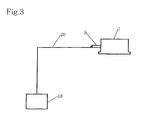
- Fig. 3 is a block diagram of a system for depressurizing the semiconductor laser module according to the first embodiment of the present invention.
- the exhaust device 18 is connected directly to the vent 9 through the piping 20.
- the tip end of the piping 20 connected to the exhaust device 18 will be mounted on the vent 9 after the lid portion 1b has been seam welded to the main body 1a of the package 1.
- the package 1 is evacuated, for example, up to about 10 -3 Torr., by the exhaust device 18 through the vent 9.
- the outer tip end of the vent 9 is swaged to provide a temporary seal.
- the swaged or adjacent portion of the vent 9 is then welded to be sealed.
- the amount of low heat conduction type gas used can be suppressed to 2-5 ml substantially equal to the internal volume of the package 1, in comparison with the prior art which required the amount of gas between 20 and 25 liters per minute.
- the first embodiment does not use any expensive noble gas in an increased amount and require any vacuum chamber or automated seam welder to be used in the vacuum chamber.
- the semiconductor laser module can inexpensively be produced through a simplified system.
- Figs. 4A and B are block diagrams of a system for introducing a low heat conduction type gas into a semiconductor laser module constructed according to a second embodiment of the present invention: Fig. 4A shows the module being evacuated and Fig. 4B shows the module into which the low heat conduction type gas is introduced.
- the second embodiment comprises first and second vents 9a, 9b mounted on the package 1 and spaced parallel apart from each other.
- the first vent 9a is used for gas exhaust while the second vent 9b is used for gas introduction.
- the exhaust device 18 is connected with the first vent 9a through a first piping 20a.
- the low heat conduction gas introducing device 19 is connected with the second vent 9b through a second piping 20b which includes an open/close valve 22.
- the tip end of the first piping 20a connected with the exhaust device 18 will be attached to the first vent 9a and the tip end of the second piping 20b connected with the low heat conduction gas introducing device 19 will be attached to the second vent 9b.
- the open/close valve 22 is in its closed position (see Fig. 4A).
- the package 1 is evacuated by the exhaust device 18 through the first vent 9a.
- the outer end of the first vent 9a is cut after it has been swaged to provide a temporary seal.
- the swaged or adjacent portion of the first vent 9a is then welded to seal it.
- the open/close valve 22 is opened to introduce the low heat conduction type gas such as xenon from the low heat conduction gas introducing device 19 into the package 1 through the second vent 9b (see Fig. 4B).
- the outer end of the second vent 9b is swaged to provide a temporary seal and cut.
- the swaged or adjacent portion of the second vent 9b is then welded to seal it.
- two branched vents that is, the first exhaust vent 9a and the second gas-introduction vent 9b, are used.
- any selector valve is not required.
- the gas exhaust and introduction can be improved in reliability.
Landscapes
- Physics & Mathematics (AREA)
- Condensed Matter Physics & Semiconductors (AREA)
- General Physics & Mathematics (AREA)
- Electromagnetism (AREA)
- Optics & Photonics (AREA)
- Optical Couplings Of Light Guides (AREA)
- Semiconductor Lasers (AREA)
- Laser Beam Processing (AREA)
Abstract
Description
Claims (19)
- A semiconductor laser module comprising:a semiconductor laser element (2) configured to produce laser light; anda package (1) being hermetically sealed and having an interior space that contains the semiconductor laser element, said package including a vent member (9) that extends from said interior space to a space that is exterior to said package, wherein,when unsealed, said vent member (9) being configured to transport a low heat conduction gas between the interior space and the exterior, andwhen sealed, said vent member (9) being configured to prevent a flow of gas between the interior space and the exterior.
- The semiconductor laser module of claim 1, wherein:said package having a first side and a second side, said second side being positioned across said interior space from said first side.said first side being configured to allow said laser light to pass therethrough, andsaid vent member (9) being disposed in said second side.
- The semiconductor laser module according to any of the preceding claims, wherein:said vent member being shaped as a pipe.
- The semiconductor laser module according to any of the preceding claims, wherein:said vent member is configured to be hermetically sealed after an occurrence of at least one of a first condition and/or a second condition.said first condition being that the low heat conductor gas has been introduced into the package via the vent member, andsaid second condition being that the low heat conduction gas has been exhausted from the package via the vent member.
- The semiconductor laser module according to any of the preceding claims, wherein:said package having a first side and a second side, said second side being positioned across said interior space from said first side;said first side being configured to allow said laser light to pass therethrough, andsaid vent member (9) being disposed in said second side; andthe vent member contains a portion that extends beyond the second side of said package, and the portion of said vent member is sealed first by being swaged and subsequently by being welded.
- The semiconductor laser module according to any of the preceding claims, wherein:Said vent member (9) is configured to receive the low heat conduction gas from a gas introducing device when said vent member is not sealed.
- The semiconductor laser module of claim 6, wherein:said vent member is configured to receive the low heat conduction gas from the gas introducing device (19) via a controllable valve (21).
- The semiconductor laser module of claim 7, wherein:said controllable valve (21) is configured to select one ofthe low heat conduction gas from the gas introducing device (19) to be provided to the package, andgas contained in the interior space of the package to be exhausted from the interior space.
- The semiconductor laser module according to any of the preceding claims, further comprising:another vent member that extends from said interior space to outside of said package, whereinsaid vent member (9b) when unsealed is configured to receive a low heat conduction gas from a gas source, andsaid another vent member (9a) when unsealed is configured to exhaust gas from said interior space.
- The semiconductor laser module according to any of the preceding claims, wherein:said vent member is configured to be sealed by being swaged close.
- The semiconductor laser module of claim 10, wherein:said vent member is configured to be permanently sealed by being welded shut after being swaged.
- A semiconductor laser module comprising:a semiconductor laser element (2) configured to produce laser light; and a package (1)being hermetically sealed and having an interior space that contains the semiconductor laser element, said package includesmeans for providing a low heat conduction gas to the interior space, andmeans for exhausting gas from the interior space.
- A method for producing a semiconductor laser module, comprising steps of:disposing a semiconductor laser element in an interior space of a package;sealing the package, except for a vent member that communicatively connects said interior space and an exterior space when open;transporting a low heat conduction gas between the interior space and the exterior space through the vent member; andhermetically sealing the vent member.
- The method of claim 13, wherein:said hermetically sealing step includes temporarily sealing the vent member by swaging a predetermined portion of said vent member that is accessible from an exterior of said package.
- The method of claim 14, wherein:said hermetically sealing step further includes welding the vent member so as to permanently seal the vent member.
- The method of claim 15, wherein:said welding step includes at least one of ultra-sonic welding and inert gas Tungsten arc welding.
- The method of any of claims 13 to 16, wherein:said transporting step includes providing the low heat conduction gas from an external gas source to the interior space via the vent member;and further comprising a step ofremoving a gas from the interior space via another vent member.
- The method of any of claims 13 to 17, wherein:said transporting step includes substeps ofevacuating a gas from the interior of the package through the vent member; andproviding the low heat conduction gas from an external gas source to the interior space via the vent member.
- The method of claim 18, wherein:said transporting step includes switching a flow direction of gas through said vent member,said switching step being performed between said evacuating step and said providing step.
Applications Claiming Priority (2)
| Application Number | Priority Date | Filing Date | Title |
|---|---|---|---|
| JP2000299638A JP4629843B2 (en) | 2000-09-29 | 2000-09-29 | Semiconductor laser module and manufacturing method and system thereof |
| JP2000299638 | 2000-09-29 |
Publications (2)
| Publication Number | Publication Date |
|---|---|
| EP1195862A2 true EP1195862A2 (en) | 2002-04-10 |
| EP1195862A3 EP1195862A3 (en) | 2004-01-02 |
Family
ID=18781418
Family Applications (1)
| Application Number | Title | Priority Date | Filing Date |
|---|---|---|---|
| EP01123597A Withdrawn EP1195862A3 (en) | 2000-09-29 | 2001-10-01 | Semiconductor laser module and method of making the same |
Country Status (4)
| Country | Link |
|---|---|
| US (1) | US6804277B2 (en) |
| EP (1) | EP1195862A3 (en) |
| JP (1) | JP4629843B2 (en) |
| CA (1) | CA2357965A1 (en) |
Cited By (3)
| Publication number | Priority date | Publication date | Assignee | Title |
|---|---|---|---|---|
| WO2003105294A1 (en) * | 2002-06-07 | 2003-12-18 | Bookham Technology Plc | Wavelength stabilized optical device |
| CN109211965A (en) * | 2018-03-12 | 2019-01-15 | 国家电投集团科学技术研究院有限公司 | Determination of conductive coefficients system |
| US10753154B1 (en) | 2019-10-17 | 2020-08-25 | Tempress Technologies, Inc. | Extended reach fluidic oscillator |
Families Citing this family (10)
| Publication number | Priority date | Publication date | Assignee | Title |
|---|---|---|---|---|
| JP2009088066A (en) * | 2007-09-28 | 2009-04-23 | Panasonic Corp | Semiconductor device |
| US8553737B2 (en) * | 2007-12-17 | 2013-10-08 | Oclaro Photonics, Inc. | Laser emitter modules and methods of assembly |
| WO2009137703A2 (en) | 2008-05-08 | 2009-11-12 | Newport Corporation | High brightness diode output methods and devices |
| TWI384713B (en) * | 2009-08-18 | 2013-02-01 | Quarton Inc | Laser module |
| EP2529452B1 (en) | 2010-01-22 | 2018-05-23 | II-VI Laser Enterprise GmbH | Homogenization of far field fiber coupled radiation |
| JP2012134350A (en) * | 2010-12-22 | 2012-07-12 | Kyocera Corp | Semiconductor device package structure |
| US8644357B2 (en) * | 2011-01-11 | 2014-02-04 | Ii-Vi Incorporated | High reliability laser emitter modules |
| WO2013084107A2 (en) * | 2011-12-05 | 2013-06-13 | Koninklijke Philips Electronics N.V. | Positioning and orientation of surgical tools during patient specific port placement |
| CN107052595A (en) * | 2017-03-28 | 2017-08-18 | 长葛市大阳纸业有限公司 | Tipping paper laser boring machine |
| US12092309B2 (en) * | 2022-08-05 | 2024-09-17 | Metro Marine Llc | Sealing a lighting fixture with dry gas |
Family Cites Families (7)
| Publication number | Priority date | Publication date | Assignee | Title |
|---|---|---|---|---|
| GB1318205A (en) * | 1970-01-30 | 1973-05-23 | Atomic Energy Authority Uk | Encapsulated electric power generators |
| JPS59177987A (en) * | 1983-03-28 | 1984-10-08 | Matsushita Electric Ind Co Ltd | Stem base body for semiconductor laser |
| US5022930A (en) * | 1989-06-20 | 1991-06-11 | Photon Energy, Inc. | Thin film photovoltaic panel and method |
| US5195102A (en) * | 1991-09-13 | 1993-03-16 | Litton Systems Inc. | Temperature controlled laser diode package |
| US5513198A (en) * | 1993-07-14 | 1996-04-30 | Corning Incorporated | Packaging of high power semiconductor lasers |
| JPH07130922A (en) * | 1993-11-01 | 1995-05-19 | Fujitsu Ltd | Semiconductor device with cooling device |
| JPH08201201A (en) * | 1995-01-31 | 1996-08-09 | Kyowa Electron Instr Co Ltd | Method of manufacturing pressure transducer |
-
2000
- 2000-09-29 JP JP2000299638A patent/JP4629843B2/en not_active Expired - Lifetime
-
2001
- 2001-09-28 CA CA002357965A patent/CA2357965A1/en not_active Abandoned
- 2001-10-01 US US09/965,863 patent/US6804277B2/en not_active Expired - Lifetime
- 2001-10-01 EP EP01123597A patent/EP1195862A3/en not_active Withdrawn
Cited By (3)
| Publication number | Priority date | Publication date | Assignee | Title |
|---|---|---|---|---|
| WO2003105294A1 (en) * | 2002-06-07 | 2003-12-18 | Bookham Technology Plc | Wavelength stabilized optical device |
| CN109211965A (en) * | 2018-03-12 | 2019-01-15 | 国家电投集团科学技术研究院有限公司 | Determination of conductive coefficients system |
| US10753154B1 (en) | 2019-10-17 | 2020-08-25 | Tempress Technologies, Inc. | Extended reach fluidic oscillator |
Also Published As
| Publication number | Publication date |
|---|---|
| US20020122446A1 (en) | 2002-09-05 |
| CA2357965A1 (en) | 2002-03-29 |
| JP4629843B2 (en) | 2011-02-09 |
| JP2002111115A (en) | 2002-04-12 |
| EP1195862A3 (en) | 2004-01-02 |
| US6804277B2 (en) | 2004-10-12 |
Similar Documents
| Publication | Publication Date | Title |
|---|---|---|
| US6804277B2 (en) | Semiconductor laser module and method of making the same | |
| US6686653B2 (en) | Miniature microdevice package and process for making thereof | |
| EP1295335B1 (en) | Miniature microdevice package and process for making same | |
| US5516031A (en) | Soldering method and apparatus for use in connecting electronic circuit devices | |
| WO2010095367A1 (en) | Vacuum sealed package, printed circuit board having vacuum sealed package, electronic device, and method for manufacturing vacuum sealed package | |
| US7940003B2 (en) | Light emitting device and method of fabricating a light emitting device | |
| KR100250778B1 (en) | Metallic evacuated double-walled vessel and production method therefor | |
| EP0382985A1 (en) | Gas purge system | |
| US8368098B2 (en) | Light emitting device and manufacturing method thereof | |
| WO2022011290A1 (en) | Small-volume uhv ion-trap package and method of forming | |
| EP1018391A1 (en) | Method and device for fuse-connection of material with high melting point | |
| KR20070069036A (en) | Semiconductor laser device and manufacturing method thereof | |
| CN101238543B (en) | Electron tube and method for manufacturing the electron tube | |
| US5088290A (en) | Transfer vessel apparatus and method of storing samples | |
| JP4401337B2 (en) | Nitride semiconductor laser light source manufacturing method and nitride semiconductor laser light source manufacturing apparatus | |
| EP0625796B1 (en) | Soldering method and apparatus for use in connecting electronic circuit devices | |
| KR20070069033A (en) | Semiconductor laser device and manufacturing method thereof | |
| JPH05343812A (en) | Semiconductor device | |
| JP2774748B2 (en) | Metal vacuum double container and method of manufacturing the same | |
| KR20160085694A (en) | Short arc type flash lamp with both ends sealed | |
| CA2410430C (en) | Miniature microdevice package and process for making thereof | |
| JP2005180723A (en) | End sealing method for heat pipe | |
| JP2637346B2 (en) | Metal vacuum double container and manufacturing method thereof | |
| JP3221113B2 (en) | Wiring forming method and apparatus | |
| US9209100B2 (en) | Housing having separate getter chamber for device operating under vacuum |
Legal Events
| Date | Code | Title | Description |
|---|---|---|---|
| PUAI | Public reference made under article 153(3) epc to a published international application that has entered the european phase |
Free format text: ORIGINAL CODE: 0009012 |
|
| 17P | Request for examination filed |
Effective date: 20011001 |
|
| AK | Designated contracting states |
Kind code of ref document: A2 Designated state(s): AT BE CH CY DE DK ES FI FR GB GR IE IT LI LU MC NL PT SE TR |
|
| AX | Request for extension of the european patent |
Free format text: AL;LT;LV;MK;RO;SI |
|
| PUAL | Search report despatched |
Free format text: ORIGINAL CODE: 0009013 |
|
| AK | Designated contracting states |
Kind code of ref document: A3 Designated state(s): AT BE CH CY DE DK ES FI FR GB GR IE IT LI LU MC NL PT SE TR |
|
| AX | Request for extension of the european patent |
Extension state: AL LT LV MK RO SI |
|
| 17Q | First examination report despatched |
Effective date: 20040524 |
|
| AKX | Designation fees paid |
Designated state(s): DE FR GB IT |
|
| STAA | Information on the status of an ep patent application or granted ep patent |
Free format text: STATUS: THE APPLICATION IS DEEMED TO BE WITHDRAWN |
|
| 18D | Application deemed to be withdrawn |
Effective date: 20041005 |