Field of the Invention
-
This invention relates to electrophotographic apparatus and, more particularly, to a novel
photoconductive member and to a method of making such a member.
Background of the Invention
-
The use of an intermediate transfer member in an electrostatographic machine to transfer
toner from an imaging member to a receiver (e.g., paper) is well known and is practiced in
commercial electrophotographic copiers and printers. A toner image formed on a primary
image-forming member (PIFM) is transferred in a first transfer operation to an
intermediate transfer member (ITM), and is subsequently transferred in a second transfer
operation from the JIM to a receiver. In the second transfer of a toner image from an ITM
roller to a receiver, a transfer back-up roller is commonly used behind a paper receiver, a
nip being formed to press the receiver to the ITM.
-
As disclosed by Rimai et al., in U.S. Patent No. 5,084,735 and Zaretsky and Gomes, in
U.S. Patent No. 5,370,961, use of a compliant ITM roller coated by a thick compliant layer
and a relatively thin hard overcoat improves the quality of electrostatic toner transfer from
an imaging member to a receiver, as compared to a non-compliant intermediate roller.
Zaretsky, in U.S. Patent No. 5,187,526, further discloses that electrostatic transfer can be
improved by separately specifying the resistivity of the ITM roller and the transfer backup
roller. Bucks et al., in U.S. Patent No. 5,701,567 disclose an ITM roller having electrodes
embedded in a compliant blanket to spatially control the applied transfer electric field.
Tombs and Benwood in U.S. Patent No. 6,075,965 disclose the use of a compliant JIM
roller in conjunction with a paper transport belt in a multi-color electrophotographic
machine.
-
For thermal transfer of toner from a photoconductor to a receiver surface, U.S. Patent
No. 5,536,609, by Jackson et al., shows the use of a compliant roller, pad or coating
behind a photoconductive belt to assist in the transfer of toner images to a receiving sheet
carried by a metal roller. The advantage of the compliant surface behind the
photoconductor is that it compresses and widens the nip for good thermal transfer and
allows the use of a hard, thermally conductive roller for carrying the receiver paper. U.S.
Patents Nos. 5,339,146 by Aslam et al., and 4,531,825 by Miwa et al., also suggest an
advantage in a compliant surface for a photoconductive member in transferring toner to a
heated, hard intermediate.
-
The use of a removable endless belt or tubular type of blanket on an intermediate roller
has long been practiced in the offset lithographic printing industry, as recently disclosed
by Gelinas in U.S. Patent No. 5,894,796 wherein the tubular blanket can be made of
materials including rubbers and plastics and can be reinforced by an inner layer of
aluminum or other metal. As disclosed earlier, for example by Julian in U.S. Patent No.
4,144,812, an intermediate lithographic roller comprises a portion having a slightly smaller
diameter than the main body of the roller, such that a blanket member can be slid along
this narrower portion until it reaches a location where a set of holes located in the roller
allow a fluid under pressure, e.g., compressed air, to pass through the holes, thereby
stretching the blanket member and allowing the entire blanket member to be slid onto the
main body of the roller. After the blanket is located in a suitable position, the source of
compressed air or fluid under pressure is turned off, thereby allowing the blanket member
to relax to a condition of smaller strain, such strain being sufficient to cause the blanket
member to snugly embrace the roller. A sleeve for a printing roller and methods for
mounting and dismounting are also disclosed in Hoage et al., U.S. Patent No. 4,903,597.
-
Vrotacoe et al., in U.S. Patent No. 5,553,541, disclose a printing blanket, for use in an
offset printing press, which includes a seamless tubular elastic layer having compressible
microspheres, surrounded by a seamless tubular layer made of a circumferentially
inextensible material, and a seamless tubular printing layer over the inextensible layer. It
is disclosed that provision of the inextensible layer reduces or eliminates pre-nip and post-nip
bulging of the roller when printing an ink image on a receiver sheet, thereby improving
image quality by reducing or eliminating ink smearing caused by slippage associated with
the formation of bulges in the prior art.
-
An intermediate transfer roller consisting of a rigid core and a removable, replaceable
intermediate transfer blanket has been disclosed by Landa et al., in U.S. Patent No.
5,335,054, and by Gazit et al., in U.S. Patent No. 5,745,829, whereby the intermediate
transfer blanket is fixedly and replaceably secured and attached to the core. The
intermediate transfer blanket, disclosed for use in conjunction with a liquid developer for
toning a primary image, consists of a substantially rectangular sheet mechanically held to
the core by grippers. The core (or drum) has recesses where the grippers are located. It
will be evident from U.S. Patent No. 5,335,054 and U.S. Patent No. 5,745,829 that owing
to the presence of the recesses, the entire surface of the intermediate transfer drum
cannot be utilized for transfer, which is a disadvantage requiring costly means to maintain
a proper orientation of the useful part of the drum when transferring a toner image from a
primary imaging member to the intermediate transfer roller, or, when transferring a toner
image from the intermediate transfer roller to a receiver. Moreover, the fact that the
blanket does not form a continuous covering of the entire core surface, owing to the fact
that two of its edges are held by grippers, is similarly a disadvantage. Another
disadvantage arises because there is inevitably a gap between these edges, so that
contamination can become deposited there which can lead to transfer artifacts.
-
Mammino et al., in U.S. Patent No. 5,298,956 and U.S. Patent No. 5,409,557, disclose a
reinforced seamless intermediate transfer member that can be in the shape of a belt,
sleeve, tube or roll and including a reinforcing member in an endless configuration having
filler material and electrical property regulating material on, around or embedded in the
reinforcing member. The reinforcing member can be made of metal, synthetic material or
fibrous material, and has a tensile modulus ranging from about 400,000 to more than
1,000,000 psi (2.8 to more than 6.9 GPa). The intermediate transfer member has a
thickness between 2 mils and about 7 mils, and a bulk resistivity less than about 1012
ohm-cm.
-
A xerographic printing sleeve mountable on a rigid drum, disclosed by Kuehnle in U.S.
Patent No. 4,255,508, includes a very thin inorganic photoconductive crystalline
compound such as cadmium sulfide coated on a thin metallic sleeve made of a suitable
metal, e.g., nickel. The thickness of the photoconductive layer is 200 -600 nanometers
and is at most of the order of one micrometer. Such a sleeve is not compliant.
-
An electrostatographic imaging member in the form of a removable replaceable endless
imaging belt on a rigid roller is disclosed by Yu et al., in U.S. Patent No. 5,415,961. The
electrostatographic imaging member is placed on the rigid roller and removed from the
rigid roller by means involving stretching the endless imaging belt with a pressurized fluid.
-
An electrostatographic imaging member that includes a photoconductive drum that has
inserted therein a compressible sleeve with the composite then being expanded to fit upon
a rigid cylindrical core support is disclosed by Swain in U.S. Patent No. 5,669,045. The
preferred sleeve is a foam that provides substantially no interference fit with the
photoconductive drum to facilitate insertion of the sleeve within the drum. However, a
relatively large interference fit exists between the rigid core and the sleeve to compress
the sleeve as it is expanded by an expandable core. The compression of the sleeve is
sufficient to render the electrostatographic imaging member substantially rigid and
substantially free from distortion. A problem with an imaging member of the type
described by Swain is that the photoconductive drum is not separately removable from the
sleeve without also removing the sleeve from the core, thereby subjecting the sleeve to
possible damage.
-
May and Tombs in U.S. Patent No. 5,715,505 and U.S. Patent No. 5,828,931 disclose a
primary image-forming member (PIFM) roller including a thick compliant blanket layer
coated on a core member, the thick compliant blanket surrounded by a relatively thin
concentric layer of a photoconductive material. The compliant primary imaging roller
provides improved electrostatic transfer of a toner image directly to a receiver member. It
is disclosed that the compliant imaging roller can be used bifunctionally, i.e., it can serve
also as an intermediate member for electrostatic transfer of a toner image to a receiver.
May and Tombs in U.S. Patent No. 5,732,311 disclose a compliant electrographic PIFM
roller.
-
U.S. Patent Nos. 5,828,931 and 5,715,505 disclose improvements in the electrostatic
transfer of toner images from a photoconductive member to a receiving surface. The
photoconductive member has a layer of compliant material having a Young's modulus
less than 5 x 10⁷ Pascals and a thin, hard photoconductive layer on the layer of compliant
material, preferably of thickness less than 15 micrometers and typically having a Young's
modulus well in excess of 108 Pascals, for example, 1010 Pascals or more. The
photoconductive members of these patents provide important advantages in the quality of
the transferred images. However, the previously known method of making such
photoconductive members has certain drawbacks. As U.S. Patent No. 5,828,931
discloses, the photoconductive member is made by coating a thin layer of a
photoconductive composition on the compliant layer surface of a cylindrical core. A
problem encountered in this operation is that the compliant layer materials, which can be,
for example, a polyurethane, silicone rubber or other elastomer typically have a low glass
transition temperature (Tg). Even when highly cross-linked, they tend to leak residue
monomers and to swell in contact with solvents used for coating the photoconductive
layer. The compliant layer, therefore, can be damaged by the coating solvent for the
photoconductive material. It can also be thermally degraded when the photoconductive
layer is heated to evaporate the solvent.
-
Another drawback of coating a photoconductive layer onto a compliant layer is that the
two layers then are adhesively bonded together. Consequently, when the photoconductive
layer, after a period of use, becomes worn and needs to be replaced, the entire assembly,
including the cylindrical core (which is typically highly toleranced and expensive), the
compliant layer and the photoconductive layer must be replaced.
-
A need exists, therefore, for a novel compliant photoconductive member and for a method
of making it that eliminates the need for coating a photoconductive layer on a compliant
layer. A need also exists for a photoconductive member in which the photoconductive
layer can be replaced when it becomes worn or at the end of its useful life, with continued
use of the core and its compliant layer.
Summary of the Invention
-
The present invention meets these needs by providing a photoconductive member that is
a novel, sleeved, compliant, electrostatographic imaging member, useful in
electrostatographic color reproduction, and a method for making such a member. The
invention a method of making of said member, and methods for using said member for
color reproduction.
-
The imaging member of the invention, preferably photoconductive, includes a central
member including a substantially rigid cylindrical first substrate or core member, a central
member having a compliant layer covering and adhered to said first substrate, and a
second substrate in the form of a flexible thin endless tubular belt having coated thereon
an imaging structure including one or more thin layers. Said second substrate and
imaging structure form a sleeve in close-fitting but non-adhesive contact with said
compliant layer.
-
In the method of making of a photoconductive imaging member of the invention a
compliant backing is made by coating a compliant layer on a first substrate, coating a
photoconductive structure including one or more layers on a second substrate, and
mounting the coated second substrate in close fitting but non-adhesive contact with the
compliant layer of the first substrate.
-
Methods of using a photoconductive imaging member of the invention include usage as a
primary image forming member and usage as a bifunctional photoconductive intermediate
transfer member in color reproduction apparatus.
-
Advantages obtained by the invention include: preventing the coating solvent used to coat
the photoconductive structure from contacting the compliant layer, thereby making a
compliant imaging member more reliably and more cheaply, and, providing replacement
of the photoconductive structure without the necessity of replacing the compliant layer and
its first substrate, thereby lowering cost and reducing downtime.
-
In accordance with the invention there is provided a photoconductive sleeved primary
image forming member roller for use in an electrophotographic machine comprising a
central member including a rigid cylindrical core member and a compliant layer formed on
the core member; and a flexible replaceable removable photoconductive sleeve member
in the form of an endless tubular belt that surrounds and nonadhesively intimately
contacts the central member.
Brief Description of the Drawings
-
In the detailed description of the preferred embodiments of the invention presented below,
reference is made to the accompanying drawings, in some of which the relative
relationships of the various components are illustrated, it being understood that orientation
of the apparatus can be modified. For clarity of understanding of the drawings, relative
proportions depicted or indicated of the various elements of which disclosed members are
included are not be representative of the actual proportions, and some of the dimensions
can be selectively exaggerated.
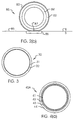
- FIG. 1
- is a schematic cross sectional view, not to scale, of a cylindrical
photoconductive member of the invention;
- FIG. 2 (a)
- is a schematic cross-sectional view, not to scale, of a photoconductive
member of the invention in pressure contact with a sheet feeding roller;
- FIG. 2 (b)
- is a schematic cross-sectional view, not to scale, of a photoconductive
member of the invention in pressure contact with a moving web;
- FIG. 3
- illustrates a cross-sectional view of a sleeve of a primary image-forming
member of the invention;
- FIG. 4 (a)
- illustrates a cross-sectional view of a preferred embodiment of a sleeve of a
primary image-forming member of the invention including a
photoconductive composite layer structure;
- FIG. 4 (b)
- illustrates a cross-sectional view of a preferred embodiment of a sleeve of a
primary image-forming member of the invention including a compliant layer
located underneath a photoconductive composite layer structure;
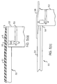
- FIG. 5 (a)
- is a schematic cross-section, with parts broken away and not to scale, of a
preferred structure for a first substrate having a compliant outer layer;
- FIG. 5 (b)
- is a schematic cross-section, with parts broken away and not to scale,
showing a photoconductive sleeve partially mounted on a less preferred
structure for a first substrate having a compliant outer layer;
- FIG. 6
- is a schematic perspective view, not to scale, of the mounting of a
photoconductor sleeve onto a sleeve mandrel to form an apparatus of the
invention;
- FIG. 7
- is a generally schematic side elevational view of an imaging apparatus
utilizing four modules, each module including a sleeved photoconductive
primary image-forming member from which a single-color toner image is
electrostatically transferred to an intermediate transfer roller, with an
endless web and web-driving mechanism for facilitating electrostatic
transfer of the single-color toner image from the intermediate transfer roller
to a receiver member adhered to and carried by the endless web through
each of the four modules, only basic components being shown for clarity of
illustration;
- FIG. 8
- is a generally schematic side elevational view of an imaging apparatus
utilizing four modules, each module including a sleeved compliant
photoconductive primary image-forming member roller with an endless web
and web-driving mechanism for facilitating electrostatic transfer of a single-color
toner image from the PIFM roller to a receiver member adhered to
and carried by the endless web through each of the four modules, only
basic components being shown for clarity of illustration;
- FIG. 9
- is a generally schematic side elevational view of an imaging apparatus
utilizing two modules, each module including a sleeved photoconductive
primary image-forming member from which a first color toner image is
electrostatically transferred in registry on top of a second color toner image
located on a compliant bifunctional intermediate transfer roller having a
photoconductive layer or layers, the second color toner image priorly
created electrophotographically on the bifunctional roller, with an endless
web and web-driving mechanism for facilitating electrostatic transfer of the
superposed first and second color toner images from the ITM roller to a
receiver member adhered to and carried by the endless web through each
of the two modules, only basic components being shown for clarity of
illustration; and
- FIG. 10
- is a diagrammatic illustration of a partly assembled inventive imaging roller
wherein the central member has marked on it a descriptive indicia located
on an outer surface of the central member in a small area located close to
an end of the central member, and the sleeve imaging member has marked
on it descriptive indicia located on the outer surface of the sleeve imaging
member in a small area located close to an end of the sleeve imaging
member, where for clarity of explanation the sleeve imaging member is
shown displaced a short distance with respect to its operational position on
the central member in order to reveal a location for an indicia on an outside
portion of the central member.
Detailed Description of the Preferred Embodiments
-
Because apparatus of the type described herein are well known, the present description
will be directed in particular to subject matter forming part of, or cooperating more directly
with, the present invention.
-
The invention relates to a novel compliant sleeved electrostatographic imaging roller
which includes a central member having a substantially rigid cylindrical first substrate or
core member, a compliant layer covering and adhered to said first substrate, and a
second substrate in the form of a thin flexible endless tubular belt having coated thereon
an imaging structure including one or more thin layers. Said second substrate and
imaging structure form a sleeve in close-fitting but non-adhesive contact with said
compliant layer.
-
A photoconductive roller of the invention utilizing a photoconductive imaging structure on
the second substrate can be conventionally charged, image-wise exposed, and toned with
particulate thermoplastic toner particles, to form a toner image on the surface of the roller.
The toner image is transferable, e.g., electrostatically, to a transferee element (TE) which
can have paper, plastic, or any other suitable receiver material. The TB can be an
intermediate transfer member (ITM) or it can be a cut receiver sheet or a continuous web.
-
The invention relates further to electrophotographic full color imaging utilizing one or more
transferable single-color toner images, whereby each single-color toner image can be
formed on a compliant sleeved primary image-forming member (SPIFM), transferred in a
first transfer step to a transferee element in the form of a compliant intermediate transfer
member (ITM), and subsequently transferred in a second transfer step to a transferee
element in the form of a receiver member, e.g., paper. Additionally, a sleeved roller of the
invention can serve bifunctionally both as an image-forming member and as a transferee
element in the form of a bifunctional photoconductive ITM, so that a transferable first
single-color toner image formed on an SPIFM can be transferred in registry on top of a
second single-color toner image independently formed on the photoconductive ITM,
thereby creating a transferable composite two-color image on the ITM which can be
subsequently transferred to a receiver sheet. An SPIFM can also be used to form a single-color
transferable toner image for direct transfer from the SPIFM to a transferee element
or to a receiver member. As an alternative to electrophotographic recording, there can be
used electrographic recording of each primary color image using stylus recorders or other
known recording methods for recording a toner image on an SPIFM which can include a
dielectric sleeve member, the transferable toner image to be transferred electrostatically
as described herein. Broadly, the primary image is formed using electrostatography, and
an SPIFM can include a web or a drum.
-
Use of a compliant SPIFM in conjunction with an JIM has several advantages in that
larger nip widths can be attained for a given pressure than if the SPIFM were non-compliant.
This in turn allows a lower transfer voltage to be used for transfer of a toner
image to an JIM, and improves image quality.
-
In prior art disclosed in Tombs and Benwood, PCT Patent Application WO 98/04961,
single-color toner images formed on conventional photoconductive drums are sequentially
transferred in registry to a receiver sheet carried on a moving transport web through a
series of corresponding single-color modules. In each module the moving transport web
frictionally drives a compliant ITM roller which in turn frictionally drives a counter-rotating
primary image forming member (PIFM) roller. Alternatively, each module can provide
transfer of a single-color toner image directly from a PIFM roller to a receiver sheet on the
transport web.
-
Generally speaking, the compliance of a layer can be considered in terms of
macrocompliance and microcompliance. In macrocompliance, the layer is able to conform
to form a nip. Microcompliance, on the other hand, comes into play at, for example, the
scale of individual toner particles, paper roughness, and edges of large toned solid areas.
Broadly speaking, an SPIFM of the invention obtains macrocompliance from the compliant
layer coated on the core member. In one of the preferred modifications described below,
microcompliance functionality can also be obtained by providing a relatively thin compliant
layer underneath the imaging structure of the sleeve.
-
It is well established that for high quality electrostatographic color imaging, small toner
particles are necessary. In the color embodiments described herein, it is preferred to use
dry, insulative toner particles having a mean volume weighted diameter of between about
2 micrometers and about 9 micrometers. The mean volume weighted diameter measured
by conventional diameter measuring devices such as Coulter Multisizer, sold by Coulter,
Inc. Mean volume weighted diameter is the sum of the mass of each particle times the
diameter of a spherical particle of equal mass and density, divided by total particle mass.
More preferably, a toner particle diameter of between 6 and 8 micrometers is employed in
the present invention. A widely practiced method of improving toner transfer is to use
toner particles including sub-micrometer particles of silica, alumina, titania, and the like,
attached or adhered to the surfaces of toner particles (so-called surface additives). In
practice of the present invention, it is preferred to use a surface additive including sub-micrometer
hydrophobic fumed silica particles, but other formulations utilizing sub-micrometer
particle surface additives can also be useful.
-
Referring now to the accompanying drawings, FIG. 7 shows an electrostatographic
imaging apparatus according to a preferred embodiment of the invention. The imaging
apparatus, designated generally by the numeral 500, is in the form of an
electrophotographic imaging apparatus and more particularly a color imaging apparatus
wherein color separation images are formed in each of four color modules and transferred
in register from toner image-bearing members to a receiver member as the receiver
member is moved through the apparatus while supported on a paper transport web (PTW)
516. A toner image-bearing member (TIBM) can include an SPIFM or an ITM, and a toner
image can be formed on it or transferred to it from another member. The apparatus
features four color modules although this invention is applicable to two or more such
modules.
-
Each module (591B, 591C, 591M, 591Y) is of similar construction except that as shown
one paper transport web 516 which can be in the form of an endless belt operates with all
the modules and the receiver member is transported by the PTW 516 from module to
module. The elements in FIG. 7 that are similar from module to module have similar
reference numerals with a suffix of B, C, M and Y referring to the color module to which it
is associated; i.e., black, cyan, magenta and yellow, respectively. Four receiver members
or sheets 512a, b, c and d are shown simultaneously receiving images from the different
modules, it being understood as noted above that each receiver member can receive one
color image from each module and that in this example up to four color images can be
received by each receiver member. The movement of the receiver member with the
PTW 516 is such that each color image transferred to the receiver member at the transfer
nip of each module is a transfer that is registered with the previous color transfer so that a
four-color image formed on the receiver member has the colors in registered superposed
relationship on the receiver member. The receiver members are then serially detacked
from the PTW and sent to a fusing station (not shown) to fuse or fix the dry toner images
to the receiver member. The PTW is reconditioned for reuse by providing charge to both
surfaces using, for example, opposed corona chargers 522, 523 which neutralize charge
on the two surfaces of the PTW.
-
Each color module of Fig. 7 includes a sleeved primary image-forming member (SPIFM),
for example a rotating hollow drum labeled 503 B, C, M and Y, respectively. The drums
rotate about their respective axes in the directions shown by the arrows. Each SPIFM
503B, C, M and Y has a compliant central member labeled 507B, C, M, Y including a
cylindrical core member having a compliant layer formed on its surface (the core and the
compliant layer formed on the core are not individually identified in Fig. 7). The central
member is snugly and non-adhesively gripped by a removable replaceable
photoconductive sleeve member in the form of an endless belt, e.g., labeled 509B, upon
which a pigmented marking particle image, or a series of different color marking particle
images, is formed. A preferred core member is rigid and is generally not solid throughout,
but preferably includes a hollow metal tube made for example from aluminum, and can
have interior structures which can include chambers, strengthening struts, and the like.
The central member preferably has a runout of less than 80 micrometers, and more
preferably less than 20 micrometers. In order to form images, the outer surface of the
photoconductive sleeve 509B of the SPIFM is uniformly charged by a primary charging
means such as a corona charging device 505 B, C, M, and Y, respectively or other
suitable charger such as roller chargers, brush chargers, etc. The uniformly charged
surface is exposed by suitable exposure means, such as for example a laser 506 B, C, M
and Y, respectively or more preferably an LED or other electro-optical exposure device or
even an optical exposure device to selectively alter the charge on the surface of the
SPIFM to create an electrostatic latent image corresponding to an image to be
reproduced. The electrostatic latent image is developed by application of pigmented
marking particles to the latent-image-bearing photoconductive drum by a development
station 581 B, C, M, and Y, respectively. The development station is a particular color of
pigmented toner marking particles associated respectively therewith. Thus, each module
creates a series of different color marking particle images on the respective
photoconductive drum. In lieu of a photoconductive drum which is preferred, a
photoconductive belt can be used.
-
Each marking particle image formed on a respective SPIFM or toner-image bearing
member (TIBM) is transferred electrostatically to an outer surface of a respective
secondary or intermediate image transfer member (ITM), for example, an intermediate
transfer drum 508 B, C, M and Y, respectively. After transfer of the toner image the
residual toner is cleaned from the surface of the photoconductive drum by a suitable
cleaning device 504 B, C, M and Y, respectively to prepare the surface for reuse for
forming subsequent toner images. Each ITM 508 B, C, M, and Y has a core member e.g.,
labeled 541 B which is preferably covered by a compliant layer formed on its surface, e.g.
labeled 542B, the compliant layer made from a suitable elastomeric material such as a
polyurethane, a silicone rubber, or other elastomers well noted in the literature. Preferably,
the compliant layer of the ITM has a thickness in a range 2 - 20 mm, and a Young's
modulus preferably less than about 10 MPa, and more preferably in a range of about 1 - 5
MPa. The silicone rubber, or other elastomers well noted in the literature. Preferably, the
compliant layer of the ITM should have a bulk electrical resistivity preferably in a range of
about 107 - 1011 ohm-cm, more preferably about 109 ohm-cm. The compliant layer 542 B,
C, Y, M is preferably coated on its outer surface by a flexible thin hard release layer (not
shown in Fig. 7) which preferably includes a synthetic material such as a sol-gel, a
ceramer, a polyurethane or a fluoropolymer, but other materials having good release
properties including low surface energy materials can also be used. The release layer has
a Young's modulus greater than 100 MPa and a thickness preferably in a range 1 - 50
micrometers, more preferably 4 - 15 micrometers. The ITM 508 B, C, M, and Y can further
include one or more sleeves. A preferred ITM core member 541 B is rigid and is generally
not solid throughout, but preferably includes a hollow metal tube made for example from
aluminum.
-
Preferably the compliant layer formed on the core member of each central member of
photoconductive imaging roller 503 B, C, M, and Y, has a thickness in a range of about
0.5 - 20 mm, and a Young's modulus preferably less than about 10 MPa, and more
preferably in a range of about 1 - 5 MPa. The compliant layer on the core member of the
central member has a Poisson's ratio in a range of about 0.2 - 0.5, and may include a
material having one or more phases, e.g., a foam or a dispersion of one solid phase in
another. Preferably, the Poisson's ratio of the compliant layer on the core is in a range of
about 0.45 - 0.50.
-
A thin protective layer may be optionally coated on the outer surface of the compliant layer
on the core of central member 507 B, C, M, and Y, to aid in removing or replacing the
imaging sleeve. This layer is preferably made from any suitable material which is flexible
and hard. It is preferred that the protective layer include a coating of a synthetic material,
preferably a creamer or a sol-gel, applied to the compliant layer by any suitable coating
method. Alternatively, the protective layer may include a thin metal band, e.g., nickel,
which may be adhered to the compliant layer on the core or which may be in the form of
an endless belt under tension applied to the outer surface of the compliant layer by, for
example, using compressed air assist, or by cooling the SB plus its compliant layer
coating in order to shrink it so as to slide on the endless metal belt. The protective layer
has a thickness preferably in a range of about 1 - 50 micrometers and more preferably in
a range of about 4 -15 micrometers, and has a Young's modulus preferably greater than
100 MPa and more preferably in a range of about 0.5 - 20 GPa.
-
Sleeve member 509B located on the SPIFM drum 503B includes a second substrate and
a photoconductive structure coated on the second substrate, which may be a backing
layer or a stiffening layer. A backing layer is defined as a layer having a Young's modulus
of 100 MPa or less, and it can be included of any suitable material, such as for example a
polymer, a fabric, a plastic, or any other material suitable as a support or backing for the
photoconductive structure. A stiffening layer is a layer having a Young's modulus greater
than 100 MPa. The second substrate is preferably conductive, and is preferably a
stiffening layer. The photoconductive structure can include one or more layers which can
include any known suitable photoconductive material, such as for example, an inorganic
material or dispersion, a homogeneous organic photoconductive layer, an aggregated
organic photoconductive layer, a composite structure including a charge generating layer
(CGL) plus a charge transport layer (CTL), and the like. In order to effect electrostatic
transfer of a toner image from SPIFM drum 503B to ITM drum 508B, it is preferred to
connect the preferably conductive second substrate of sleeve 509B to ground potential, in
which case the second substrate preferably has a bulk or volume electrical resistivity of
less than about 1010 ohm-cm. However, in some applications it can be desirable to use a
non-conductive stiffening layer (SL), in which case the second substrate can be coated
with a thin conductive material, e.g., a metallic film applied to the surface of the second
substrate, which is connected to ground potential.
-
A preferred sleeve member 509B located on the SPIFM drum 503B includes a stiffening
layer, a barrier layer coated on the SL, a charge generating layer (CGL) coated on the
barrier layer, and a charge transport layer (CTL) coated on the CGL [see for example
FIG. 4(a)]. The stiffening layer preferably has the form of an endless tubular belt. More
preferably, the stiffening layer is a seamless belt. The SL, which preferably has a high
modulus and therefore is substantially inextensible, provides a useful function by
minimizing hoop strain in the underlying compliant layer 507B. Preferably, the stiffening
layer (SL) is thin and flexible and includes any suitable conductive material, such as a
metal, e.g., steel, nickel, brass or other high tensile metal. Less preferably, the SL can
include an elastomer such as for example a polyurethane doped with a conductive
material such as an antistat, or a synthetic polymeric or plastic material including a
dispersion of conductive particles having a volume fraction above the percolation
threshold, the SL having a yield strength which is not exceeded during operation of the
SPIFM. A stiffening layer of sleeve 509 B, C, Y, M has a thickness less than about 500
micrometers, preferably in a range of about 10 - 200 micrometers, and a Young's modulus
greater than about 0.1 GPa, preferably in a range of about 50 - 300 GPa. It is preferred
that the stiffening layer is made of nickel in the form of an electroformed seamless belt
0.005 inch thick available, e.g., from Stork Screens America, Inc., of Charlotte, North
Carolina. The preferred photoconductive structure coated on the SL includes: a polyamide
resin barrier layer having thickness greater than about 0.5 micrometer and preferably
greater than 1.0 micrometer; a CGL of the type described by Molaire et al. in U.S. Patent
No. 5,614,342 including a co-crystal dispersion with the CGL coated on the barrier layer,
the CGL having a thickness in a range 0.5 - 1.0 micrometer and preferably about 0.5
micrometer; and a CTL, coated on the CGL, having thickness 12 - 35 micrometers and
preferably about 25 micrometers, the CTL having equal parts of tri-tolylamine and 1,1-bis{4-(di-4-tolylamino)phenyl}methane
in a binder consisting of 20% wt/wt poly[4,4'-(2-norbornylidene)bisphenol
terephthalate-co-azelate-(60/40)] and 80% wt/wt MakrolonTM
polycarbonate obtainable from General Electric, Schenectady, NY.
-
In another preferred embodiment, microcompliance can be provided to the sleeve 509B
by including a thin compliant layer (CL) coated on a stiffening layer underneath the CGL
and the CTL coatings, the thin CL having a thickness preferably in a range 0.5 - 2.0
micrometers. A thin conductive layer, e.g., of nickel, can be coated on top of the thin CL,
upon which are successively coated an optional barrier layer, a CGL, and a CTL, as
described above [see for example FIG. 4(b)]. Preferably the thin conductive layer is
grounded during operation. Alternatively, the thin CL can be coated by an optional charge
injection barrier layer and the CL provided with suitable electrical conductivity so as to be
usable with a grounded conductive core member.
-
In some applications an optional thin hard wear resistant layer can be provided as an
exterior coating outside the CTL, such as for example having a sol-gel, silicon carbide,
diamond-like carbon, or the like.
-
A single-color marking particle image respectively formed on the ITM roller 508B is
transferred to a toner image receiving surface of a receiver member, which is fed into a
nip between the intermediate image transfer member drum and a transfer backing roller
(TBR) 521B, C, M, and Y, respectively, that has an outer resistive blanket and is suitably
electrically biased by power supply 552 to induce the charged toner particle image to
electrostatically transfer to a receiver sheet. The receiver member is fed from a suitable
receiver member supply (not shown) and is suitably "tacked" to the PTW 516 and moves
serially into each of the nips 510B, C, M, and Y where it receives the respective marking
particle image in suitable registered relationship to form a composite multicolor image. As
is well known, the colored pigments can overlie one another to form areas of colors
different from that of the pigments. The receiver member exits the last nip and is
transported by a suitable transport mechanism (not shown) to a fuser where the marking
particle image is fixed to the receiver member by application of heat and/or pressure and,
preferably both. A detack charger 524 can be provided to deposit a neutralizing charge on
the receiver member to facilitate separation of the receiver member from the belt 516. The
receiver member with the fixed marking particle image is then transported to a remote
location for operator retrieval. The respective ITMs are each cleaned by a respective
cleaning device 51 1B, C, M, and Y to prepare it for reuse.
-
Appropriate sensors (not shown) of any well known type, such as mechanical, electrical,
or optical sensors for example, are utilized in the imaging apparatus 500 to provide control
signals for the apparatus. Such sensors are located along the receiver member travel path
between the receiver member supply through the various nips to the fuser. Further
sensors can be associated with the primary image forming member photoconductive
drum, the intermediate image transfer member drum, the transfer backing member, and
various image processing stations. As such, the sensors detect the location of a receiver
member in its travel path, and the position of the primary image forming member
photoconductive drum in relation to the image forming processing stations, and
respectively produce appropriate signals indicative thereof. Such signals are fed as input
information to a logic and control unit LCU including a microprocessor, for example.
Based on such signals and a suitable program for the microprocessor, the control unit
LCU produces signals to control the timing operation of the various electrographic process
stations for carrying out the imaging process and to control drive by motor M of the
various drums and belts. The production of a program for a number of commercially
available microprocessors, which are suitable for use with the invention, is a conventional
skill well understood in the art. The particular details of any such program would, of
course, depend on the architecture of the designated microprocessor.
-
FIG. 10 is a sketch of a cutaway end portion of an assembly, indicated as 90, of a
photoconductive sleeve 92 concentrically disposed on a central member 91 of an
inventive roller. Central member 91 has marked on it descriptive indicia located on its
outer surface in a small area located close to an end of the central member, and the
photoconductive sleeve 92 has marked on it descriptive indicia located on its outer
surface in a small area located close to an end of the photoconductive sleeve. For clarity
of explanation, the photoconductive sleeve is shown displaced from its operational
location by a short distance with respect to the central member in order to reveal a
location for an indicia on an outside portion of the central member. The indicia are
provided on the photoconductive sleeve to indicate a parameter relative to the
photoconductive sleeve, and are also provided on the central member to indicate a
parameter relative to the central member. With reference to Fig. 10, entities shown therein
that are similar to one another are identified with one or more primes (') after the reference
numbers. The indicia on the central member, i.e., a set of descriptive markings, can be
located in a preferably small area 93" located on a cylindrically curved portion of the
central member close to an end of the central member. More preferably, the indicia on the
central member are contained in a preferably small area 93' located on an end of central
member 91 and close to the perimeter (the individual layers having central member 91 are
not shown). The indicia on the photoconductive sleeve member, i.e., a set of descriptive
markings, are preferably located in a small area 93" located on a cylindrically curved
portion of the photoconductive sleeve member close to an end of the photoconductive
sleeve member. More preferably, the indicia on the photoconductive sleeve member are
contained in a small area 93" located on an end of sleeve 92 (the individual layers having
sleeve 92 are not shown). An enlarged view 93 of any one of the small areas 93', 93",
93'", or 93"" illustrates that the descriptive indicia can be in the form of a bar code, as
indicated by the numeral 94, which can be read, for example, by a scanner. The scanner
can be mounted in an electrophotographic machine so as to monitor an inventive roller,
e.g., during operation of the machine or during a time when the machine is idle, or the
scanner can be externally provided during installation of, or maintenance of, an inventive
roller. Generally, the indicia can be read, sensed or detected by an indicia detector 95. As
indicated in Fig. 10 by the dashed arrow labeled B, the analog or digital output of the
indicia detector can be sent to a logic control unit (LCU) incorporated in an
electrostatographic machine utilizing an inventive photoconductive roller, or it can be
processed externally, e.g., in a portable computer during the installation or servicing of an
inventive photoconductive roller, or it can be processed in any other suitable data
processor. The indicia can be read optically, magnetically, or by means of radio
frequency. In addition to a bar code 94, the indicia can include any suitable markings,
including symbols and ordinary words, and can be color coded. The indicia can also be
read visually or interpreted by eye. A color coded indicia on a member can include a
relatively large colored area which can be otherwise devoid of markings or other features
and which can readily be interpreted by eye to indicate a predetermined property of the
color-coded member. Suitable materials for the indicia are for example inks, paints,
magnetic materials, reflective materials, and the like, which can be applied directly to the
surface of the sleeve member. Alternatively, the indicia can be located on a label that is
adhered to the outer surface of the sleeve member. The indicia can also be in raised form
or produced by stamping with a die or by otherwise deforming a preferably small local
area on the outer surface of the sleeve member, and the deformations can be sensed
mechanically or otherwise detected or read using an indicia detector 95 in the form of a
contacting probe or by other mechanical means. It can also be desirable for some
applications to place indicia on the inner surface of sleeve member 92. It can also be
desirable to provide a cutaway or an opening in sleeve member 92 so that an indicia
located in an area 93" on central member 91 can be detected when the outer sleeve is
located in operational position, and not displaced as shown in Fig. 10.
-
Different types of information can be encoded or recorded in the indicia on the central
member and on the photoconductive sleeve. For example, the outside diameter of a roller,
i.e., the outside diameter of the photoconductive sleeve member can be recorded so that
nip width or registration parameters can be accordingly adjusted. The effective hardness
and effective Young's modulus of a sleeve or central member of an inventive roller can be
recorded in the indicia so that nip widths can be suitably adjusted. The date of
manufacture of the sleeve or central member of the roller can be recorded in the indicia
for diagnostic purposes, so that the end of useful life of the given sleeve or central
member could be estimated for timely replacement. Specific information for each given
roller regarding the roller runout, e.g., as measured after manufacture, can also be
recorded in the indicia, and this information could be used for optimizing registration, e.g.,
between modules. Moreover, the orientation of an inventive roller, such as for example a
skew between an inventive roller and an intermediate transfer roller, can be described by
the indicia.
-
When the outside diameter of the photoconductive sleeve of an inventive roller is recorded
in the indicia, the information can be used to speed the calibration time of a registration
system as explained below. For example, the registration system can utilize a software
algorithm that controls the speed of the start-of-line clock signal fed to an LED writehead.
A separate start-of-line clock signal is used for each color module, each controlling the
length of the color toner image of the respective color separation image produced by each
module, thereby ensuring that the color toner image length is correct and uniform
throughout the image. It is known that, in general, a change in the engagement between a
primary imaging roller and an ITM roller changes the speed ratio, thereby altering the
length of the image, e.g., by stretching or compressing it as the engagement is increased
or decreased. Photoconductive sleeve members cannot be manufactured practically with
identical outside diameters, a typical variation being ± 50 micrometers. A small difference
in the diameter of a newly installed photoconductive sleeve of an inventive roller can,
therefore, effectively change the engagement between the primary imaging and ITM
rollers (for the same applied force between the rollers). Similar changes of engagement
can be caused by a manufacturing variability of central members. By utilizing the diameter
information of a newly installed photoconductive sleeve, the registration unit can
immediately correct the start-of-line clock signal so that the image length and uniformity is
maintained correctly. This adjustment of the parameters in the algorithm controlling the
start-of-line clock signal is one of several parameters that need to be controlled to ensure
accurate registration of each digital image written by the writehead. Prior knowledge of the
outside diameter of an inventive photoconductive sleeved roller given in the indicia speeds
the calibration time of the registration system.
-
The receiver members utilized with the reproduction apparatus 500 can vary substantially.
For example, they can be thin or thick paper stock, or transparency stock, e.g., plastic
sheets. As the thickness and/or bulk resistivity of the receiver member stock varies, the
resulting change in impedance affects the electric field used in the nips 510B, C, M, Y to
urge transfer of the marking particles to the receiver members. Moreover, a variation in
relative humidity will vary the conductivity of a paper receiver member, which also affects
the impedance and hence changes the transfer electric field.
-
The endless belt or web (PTW) 516 is preferably included of a material having a bulk
electrical resistivity greater than 105 ohm cm and where electrostatic hold down of the
receiver member is not employed, it is more preferred to have a bulk electrical resistivity
of between 108 ohm cm and 1011 ohm cm. Where electrostatic hold down of the receiver
member is employed, it is more preferred to have the endless web or belt have a bulk
resistivity of greater than 1 x 10¹² ohm-cm. This bulk resistivity is the resistivity of at least
one layer if the belt is a multilayer article. The web material can be of any of a variety of
flexible materials such as a fluorinated copolymer (such as polyvinylidene fluoride),
polycarbonate, polyurethane, polyethylene terephthalate, polyimides (such as Kapton™),
polyethylene napthoate, or silicone rubber. Whichever material that is used, such web
material can contain an additive, such as an anti-stat (e.g. metal salts) or small conductive
particles (e.g. carbon), to impart the desired bulk resistivity for the web. When materials
with high bulk resistivity are used (i.e., greater than about 1011 ohm cm), additional corona
charger(s) can be needed to discharge any residual charge remaining on the PTW once
the receiver member has been removed. The PTW can have an additional conducting
layer beneath the resistive layer which is electrically biased to urge marking particle image
transfer, however, it is more preferable to have an arrangement without the conducting
layer and instead apply the transfer bias through either one or more of the support rollers
or with a corona charger. The endless belt is relatively thin (20 micrometers - 1000
micrometers, preferably, 50 micrometers - 200 micrometers) and is flexible. It is also
envisioned that the invention applies to an electrostatographic color machine wherein a
generally continuous paper web receiver is utilized and the need for a separate paper
transport web is not required. Such continuous webs are usually supplied from a roll of
paper that is supported to allow unwinding of the paper from the roll as the paper passes
as a generally continuous sheet through the apparatus.
-
In feeding a receiver member onto belt 516 charge can be provided on the receiver
member by charger 526 to electrostatically attract the receiver member and "tack" it to the
belt 516. A blade 527 associated with the charger 526 can be provided to press the
receiver member onto the belt and remove any air entrained between the receiver
member and the belt.
-
A receiver member can be engaged at times in more than one image transfer nip and
preferably is not in the fuser nip and an image transfer nip simultaneously. The path of the
receiver member for serially receiving in transfer the various different color images is
generally straight facilitating use with receiver members of different thicknesses.
-
The endless paper transport web (PTW) 516 is entrained about a plurality of support
members. For example, as shown in Fig. 7, the plurality of support members are rollers
513, 514 with preferably 513 being driven as shown by motor M (of course, other support
members such as skis or bars would be suitable for use with this invention). Drive to the
PTW can frictionally drive the ITM rollers to rotate the ITMs which in turn causes the
SPIFM rollers to be rotated, or additional drives can be provided. The process speed is
determined by the velocity of the PTW which can be any useful velocity, typically about
300 mm/sec.
-
Support structures 575a, b, c, d, and e are provided before entrance and after exit
locations of each transfer nip to engage the belt on the backside and alter the straight line
path of the belt to provide for wrap of the belt about each respective ITM roller so that
there is wrap of the belt of greater than 1 mm on each side of the nip (pre-nip and post-nip
wraps) or at least one side of the nip and preferably the total wrap is less than 20 mm.
The nip is where the pressure roller contacts the backside of the belt or where no
pressure roller is used, where the electrical field is substantially applied. However, the
image transfer region of the nip is a smaller region than the total wrap. The wrap of the
belt about the ITM roller also provides a path for the lead edge of the receiver member to
follow the curvature of the ITM but separate from engagement with the ITM while moving
along a line substantially tangential to the surface of the cylindrical ITM. Pressure applied
by the transfer backing rollers (TBRs) 521 B, C, M, and Y is upon the backside of the belt
516 and forces the surface of the compliant JIM to conform to the contour of the receiver
member during transfer. Preferably, the pressure of each TBR 521 B, C, M, and Y on the
PTW 516 is 7 pounds per square inch or more. The TBRs can be replaced by corona
chargers, biased blades or biased brushes. Substantial pressure is provided in the
transfer nip to realize the benefits of the compliant intermediate transfer member which
are conformation of the toned image to the receiver member and image content on both a
microscopic and macroscopic scale. The pressure can be supplied solely by the transfer
biasing mechanism or additional pressure applied by another member such as a roller,
shoe, blade or brush.
-
It is to be understood in Fig. 7 that the amount of pre-nip wrap and post-nip wrap can be
set to any convenient values in any of the modules, and can be made to differ module to
module by adjustments of the individual elevations of individual support structures or by
placing the support structures at points that are not half-way between modules, or both.
-
Moreover, in order to have independent control of the amounts of pre-nip and post-nip
wrap within each module, a larger number of support structures can be used, e.g., two
support structures per module, one on each side of each transfer nip. Support structures
can include skids, bars, rollers, and the like.
-
With reference to FIG. 8, structures shown therein that are similar to structures in FIG. 7
are identified with a prime (') after the reference numbers. In the embodiment of FIG. 8, a
toner color separation image of one of each of four colors is formed by each module
591B', 591C', 591M', and 591Y' on respective sleeved primary image forming member
photoconductive drums 503B', 503C', 503M', and 503Y', each drum having a removable
replaceable photoconductive sleeve 509B', 509C', 509M', and 509Y' and a compliant
central member 507B', 507C', 507M', and 507Y'. In Fig. 8 the dimensions and electrical
and physical properties of the SL, CGL and CTL of the photoconductive sleeve 509B',
509C', 509M', and 509Y' are similar to those in the preferred embodiments previously
described above for the sleeve 509B, 509C, 509M, and 509Y in Fig. 7. The respective
toned color separation images are transferred in registered relationship to a receiver
member as the receiver member serially travels or advances from module to module
receiving in transfer at each transfer nip (510B' is the only nip designated) a respective
toner color separation image. In the embodiment of FIG. 8, the ITMs are not present and
direct transfer of each image is made from the respective sleeved photoconductive drums
to the receiver sheet as the receiver sheet serially advances through the transfer stations
while supported by the paper transport web 516'. In the preferred embodiment for direct
transfer of toner images from SPIFMs to receiver sheets, microcompliance is provided to
the photoconductive sleeve 509B' by including a thin compliant layer coated on the SL
underneath the CGL and the CTL coatings, the thin CL having a thickness preferably in a
range 0.5 - 2.0 micrometers. The preferred electrical and physical properties are similar to
those in the embodiment previously described above for the thin CL of an embodiment of
sleeve 509B in Fig. 7. A thin conductive layer, e.g., of nickel, can be coated on top of the
thin CL, upon which are successively coated an optional barrier layer, a CGL, and a CTL,
as also described above. The thin conductive layer is preferably grounded during
operation.
-
In another preferred embodiment, the number of modules required for full color imaging is
reduced by utilizing compliant sleeved primary image forming members (SPIFMs) as
bifunctional photoconductive ITMs. With reference to FIG. 9, structures shown therein that
are similar to structures in FIGS. 7 and 8 are identified with a double prime (") after the
reference numbers. In the embodiment of FIG. 9, an apparatus designated by the numeral
600 includes two modules 691BC and 691MY, although a different number of modules
can be employed. Each module is of similar construction except that as shown one paper
transport web 516" which can be in the form of an endless belt operates with all the
modules, and receiver members 512a", 512b", 512c", and 512d" are transported by the
PTW 516" from module to module. Module 691BC for example includes a rotating
photoconductive SPIFM drum 603B engaging a counter-rotating bifunctional
photoconductive ITM drum 608BC in a pressure nip indicated by the label 610B, the drum
608BC also engaged in a pressure nip indicated as 610BC produced by TBR 621 BC
behind the paper transport web 516", the PTW frictionally driving the drum 608BC.
Movement of PTW 516" is indicated by an arrow. SPIFM drum 603B includes a compliant
central member 607B further including a rigid cylindrical core member with a compliant
layer formed on it, and a removable replaceable photoconductive sleeve imaging member
609B preferably nonadhesively gripping and surrounding the central member.
Photoconductive drums 603B and 608BC have material characteristics similar to those for
drums 503B, C, M and Y described above. On each of the drums 603B, 608BC, 603M,
and 608MY a different single-color toner image is formed, made for example from black,
cyan, magenta, and yellow toners indicated by the letters B, C, N, and Y, respectively, or
from different colors, or a different number of colors. Also, toners including non-color
attributes can be used. In module 691BC, a black toner image is formed on
photoconductive drum 603B, using charger 605B, laser 606B and development station
681B, and a cyan toner image is formed on photoconductive drum 608BC, using charger
605C, laser 606C and development station 681C. The black toner image is
electrostatically transferred in the nip 610B from drum 603B to the drum 608BC such that
the black toner image is transferred on top of the cyan image, thereby forming a
registered first composite image. Rotary motion of drum 608BC brings the first composite
image into the nip 610BC where the first composite image is electrostatically transferred
to a receiver sheet, such as for example the paper sheet 512b". In module 691 MY, a
magenta toner image created on SPIFM 603M and a yellow toner image created on
photoconductive ITM 608MY are similarly combined in nip 610M to form a second
composite image which is transferred on top of the first composite image in nip 610MY to
create a registered four-color composite toner image on the receiver sheet.
-
Prior to forming single-color toner images on photoconductive drums 603B, 608BC, 603M,
and 608MY, the outer surfaces of the respective sleeves are cleaned by the respective
cleaning stations 604B, C, M, and Y.
-
In the three embodiments of FIGS. 7, 8, and 9, the transfer backing rollers 521, 521', and
621 BC have a preferred diameter of 20 - 80 mm, preferably running in a constant current
mode. The diameters of the SPIFM and ITM members are preferably in the range of 80 -
240 mm. Also, in the three machine embodiments of FIGS. 7, 8, and 9, different receiver
sheets can be located in different nips simultaneously and at a times one receiver sheet
can be located in two adjacent nips simultaneously, it being appreciated that the timing of
image creation and respective transfers to the receiver sheet is such that proper transfer
of images are made so that respective images are transferred in register and as expected.
-
Although it is preferred to be a drum, an ITM in the form of a web can be used with an
SPIFM in the color reproduction apparatus described herein. Similarly, an SPIFM in the
form of a web can be used, although not preferred.
-
In the color reproduction apparatus described herein, the apparatus can also be used to
form color images in various combinations of color in lieu of the four-color image
described. Fewer color modules can be provided in the apparatus or additional color
modules can be provided in the apparatus. While the description herein is directed to
formation of a composite resultant image on a receiver sheet formed of plural color
images, the invention contemplates that images of different physical types of toner can be
combined on a receiver sheet to form a composite resultant image. Thus, a black toner
image can be transferred to a receiver sheet wherein the toner image is formed of nonmagnetic
toner and a second black image formed on the same receiver sheet using a
magnetic toner using the transfer apparatus and methods described herein.
-
In the described embodiments, the wrap of the belt that supports the receiver member in
contact with the toner image bearing member (TIBM) is defined by tension in the transport
belt. The actual transfer nip where the major portion of the electrical field exists between
the TIBM and the transfer backing roller or other counter electrode for transfer of the toner
image to the receiver member is smaller than this wrap. Thus, by providing a greater
amount of wrap length than the length of the actual transfer nip there is reduced the
likelihood of pre-nip transfer and pre-nip ionization particularly where the transport belt is
substantially insulative. As noted above, it is preferred to have the wrap be greater than 1
mm beyond the roller nip in at least the pre-nip area. Where a transfer backing pressure
roller is used to apply the pressure to the underside of the belt to urge the receiver
member into intimate contact with the TIBM at the nip, it is preferred that the pressure
roller be of intermediate conductivity, i.e., bulk resistivity of 107 - 1011 ohm/cm; however,
transfer backing rollers that are highly conductive, i.e., having conductivity of a metal, also
can be used. Other structures, as noted above, in lieu of transfer backing rollers can be
used to apply pressure to the web at the nip including members having conductive fibers
that are electrically biased and provided with stiffener structure on either side of the brush
for applying pressure to the web, or rollers with conductive fibers.
-
In the embodiments described above, transfer of the toner image from the SPIFM to the
ITM and from the ITM to the receiver member and generally all toner image transfers are
made electrostatically and preferably without addition of heat that would cause the toner
to soften. Thus, preferably no fusing occurs upon transfer of the toner images to the
receiver member in the nips through which the paper transport belt and receiver member
passes. In the forming of plural color images in registration on a receiver sheet, the
invention contemplates that plural color toner images can be formed on the same image
frame of the photoconductive image member using well known techniques; see, for
example Gundlach, U.S. Patent No. 4,078,929. The primary image forming member can
form images by using photoconductive elements as described or dielectric elements using
electrographic recording. The toners used for development are preferably dry toners that
are preferably nonmagnetic and the development stations are known as two-component
development stations. Single component developers can be used, but are not preferred.
While not preferred, liquid toners can also be used.
-
Other charging means such as rollers can be used instead of the corona wire chargers
used for electrostatically holding the receiver member or print media to the web ("tacking")
and also for electrically discharging the receiver member.
-
Cleaning of the front side and back side of the PTW belt can be provided by wiper blades
560a and 562a (FIG. 7), 560a', 562a' (FIG. 8), or 560a", 562a" (FIG. 9), respectively. It is
preferred to use wiper blades for both of the front and backside cleaning.
-
Additional thin coating layers (not indicated in any of the FIGS.) for promoting inter-layer
adhesion can be employed in the fabrication of sleeve members, such as for example
priming or subbing layers well known in the art can be used.
-
In order to promote placement or removal of a sleeve of the invention, submicron particles
of silica, titania and the like can be applied to the outer surface of a central member, to an
inner surface of a sleeve member. Alternatively, a surface region having a thickness of the
order of a few molecular dimensions and chemically selected or modified to include
chemical molecular groups exhibiting a low surface energy can be provided on these
surfaces (not indicated in any of the figures).
-
The invention discloses a sleeved photoconductive primary-image-forming member roller
for use in an electrostatographic machine. A sleeve member is placeable on a compliant
central member by a sleeve placement method, and is removable from the central
member by a sleeve removal method, the sleeve member retaining a form of an endless
belt not only during operation of the SPIFM, but also during placement of a sleeve
member or during removal of a sleeve member. In one of the preferred embodiments, the
SPIFM can be used as a bifunctional photoconductive ITM.
-
A preferred sleeve placement method includes providing a source of a pressurized fluid to
the underside of a sleeve member, the preferred pressurized fluid being compressed air;
turning on the source of the pressurized fluid to elastically expand the sleeve member so
as to allow the sleeve member to be moved along the surface of a central member in
order to surround the central member; continuing to keep open the source of pressurized
fluid while sliding the sleeve member to be moved until it reaches a predetermined
position surrounding the other member; shutting off the source of the pressurized fluid,
thereby allowing the sleeve member to relax and grip the said another member under
tension. Other methods of aiding sleeve placement can be used, including separately
heating the sleeve member being placed on a central member, or separately cooling the
substrate, in order to take temporary advantage of dimensional changes produced by the
heating or cooling.
-
A preferred sleeve removal method includes providing a source of a pressurized fluid to
the underside of a sleeve member, the preferred pressurized fluid being compressed air;
turning on the source of the pressurized fluid to elastically expand the sleeve member so
as to allow the sleeve member to be moved along the surface of a central member;
continuing to keep open the source of pressurized fluid while sliding the sleeve member
and removing it from the central member; shutting off the source of the pressurized fluid.
Other methods of aiding sleeve removal can be used, including separately heating the
sleeve member being removed from the central member, or separately cooling the
substrate, in order to take temporary advantage of dimensional changes produced by the
heating or cooling.
-
Turning now to preferred embodiments having electrostatographic and photoconductive
sleeved imaging rollers of the invention, FIG. 1 shows a cross-sectional view, indicated by
the numeral 10, of an electrophotographic sleeve imaging member identified by the
numeral 17 which is mounted on a central member identified by the numeral 14. The
central member 14 is included of a first substrate or core member 11, a compliant layer 12
formed on the core member, and an optional protective layer 13 coated on the compliant
layer. Central member 14 has a smooth surface, and preferably has a runout of less than
80 micrometers and more preferably less than 20 micrometers. The sleeve member 17 is
preferably in the form of an endless seamless tubular belt, and is included of a second
substrate or stiffening layer 15 and a photoconductive structure 16 coated on the second
substrate.
-
The preferred core member 11 is substantially rigid and is generally not solid throughout,
and as shown in FIG. 1 preferably includes a hollow cylindrical metal tube or shell made
for example from aluminum. Core member 11 can have interior structures which can
include chambers, e.g., for compressed air and associated piping, strengthening struts,
and the like, and can be provided with holes for carrying compressed air from an interior
chamber through its cylindrical shell during placement or removal of the sleeve
member 17. The compliant layer (CL) 12 of central member 14 preferably has a thickness
in a range of about 0.5 - 20 mm, and a Young's modulus preferably less than about 10
MPa and more preferably in a range of about 1 - 5 MPa. The CL 12 is preferably formed
of a polymeric material, e.g., an elastomer such as a polyurethane or other materials well
noted in the published literature. The CL 12 has a Poisson's ratio in a range 0.2 - 0.5, and
can include a material having one or more phases, e.g., a foam or a dispersion of one
solid phase in another. Preferably, CL 12 has a Poisson's ration between about 0.45 and
0.50.
-
The optional protective layer 13 is preferably made from any suitable material which is
flexible and hard, e.g., a synthetic material, preferably a ceramer or a sol-gel, applied to
the compliant layer 12 by any suitable coating method. Alternatively, the protective layer
13 can include a thin metal band, e.g., nickel, which can be adhered to the CL 12 or which
can be in the form of an endless belt under tension applied to the outer surface of the CL
12 by, for example, using compressed air assist, or by mounting the central member on a
mandrel and cooling in order to shrink it so as to slide on the metal band. The protective
layer 13 has a thickness preferably in a range 1 - 50 micrometers and more preferably in a
range 4 - 15 micrometers, and a Young's modulus preferably greater than 100 MPa and
more preferably in a range 0.5 - 20 GPa.
-
In Fig. 2(a) of the drawings, the photoconductive member 10 of Fig. 1 is shown in contact
with a sheet feeding roller or back-up roller 20 which exerts pressure against
photoconductive member 10 and causes the compliant layer 12 of the central member to
deform at the nip between roll 20 and flexible photoconductive sleeve 17 and form an
enlarged area of contact 21 (layer 13 omitted). As the member 10 and the roller 20 rotate
on their longitudinal axes in the directions shown by arrows 22 and 23 a sheet of paper or
other toner receiving sheet material is fed into the nip for electrostatic transfer of toner to
the receiving sheet. Because of the enlarged nip area formed by the compliant layer 12,
the electrostatic transfer of toner to the receiving sheet is markedly improved as compared
with transfer from a conventional photoconductive imaging drum.
-
Another way of employing the photoconductive member of the invention is shown by Fig.
2(b). In this embodiment, the photoconductive member 80 has a first substrate which is a
rigid hollow cylinder or core 84. On this substrate is coated the compliant layer 82 and
mounted on the latter in a close-fitting but non-adhesive relationship is a sleeve 83 having
a thin-walled nickel tube (not shown) on which is coated the thin photoconductive layer
(not shown). Fig. 2(b) illustrates the transfer of toner from photoconductive member 80 to
a continuous web of paper, plastic or other material 85. The web 85 is drawn across a
backing member 86 against which the photoconductive member presses to cause
flattening of the compliant layer 82 and consequent enlargement of the nip area 87 where
electrostatic transfer of toner from photoconductive layer 84 to the moving web 85 occurs.
Backing member 86 can be a roller, a skid, a bar, or the like.
-
FIG. 3 illustrates a photoconductive sleeve member identified as 30 which is useful for an
SPIFM drum. Sleeve 30 is preferably an endless tubular belt and includes a second
substrate layer 31 and a photoconductive structure 32 surrounding and adhered to the
second substrate layer. Sleeve 30 can also include a compliant layer (not separately
indicated in Fig. 3) preferably located underneath the photoconductive structure 32. The
photoconductive structure can include one or more layers which can include any known
suitable photoconductive material, such as for example, an inorganic material or
dispersion, a homogeneous organic photoconductive layer, an aggregated organic
photoconductive layer, a composite structure having a charge generating layer (CGL) plus
a charge transport layer (CTL), and the like. The second substrate 31 is preferably
conductive with a bulk or volume electrical resistivity of less than about 1010 ohm-cm, and
connectable to ground potential. However, in some applications it can be desirable to use
a non-conductive second substrate layer, in which case SL 31 can be coated with a thin
conductive material, e.g., a metallic film, applied its surface, which is connectable to
ground potential. The second substrate layer 31 includes any suitable flexible material.
The second substrate layer can include a sheet formed in to an endless tube joined by a
seam to create an endless belt, but a seamed second substrate is less preferred.
Preferably, the second substrate has a form of an endless seamless belt. The second
substrate can be a backing layer or a stiffening layer. A backing layer, which is less
preferred for the second substrate, can be included of any suitable material having a
Young's modulus of 100 MPa or less, such as for example a polymer, a fabric, a plastic,
or any other material suitable as a support or backing for the photoconductive structure. A
stiffening layer (SL) is preferred for the second substrate. The SL has a thickness less
than 500 micrometers and more preferably in a range of about 10 - 200 micrometers. The
SL in general should have a yield strength which is not exceeded during operation of the
SPIFM, with the stiffening layer remaining as a continuous belt and which does not crack
or break up into platelets. The stiffening layer also has a Young's modulus preferably
greater than about 0.1 GPa and more preferably in a range of about 50 -300 GPa.
-
FIG. 4(a) shows a preferred embodiment of a photoconductive sleeve as indicated by a
composite structure 40A, which includes a stiffening layer 41, a barrier layer 42 coated on
the stiffening layer, a charge generating layer (CGL) 43 coated on the barrier layer, and a
charge transport layer (CTL) 44 coated on the CGL. Sleeve 40A is preferably an endless
tubular belt. The stiffening layer (SL) 41 is preferably an endless tubular belt, and more
preferably is a seamless belt. The stiffening layer can include any suitably flexible material
having a thickness less than 500 micrometers and more preferably in a range of about 10
- 200 micrometers, and a Young's modulus greater than about 100 MPa and more
preferably in a range of about 50 - 300 GPa. More preferably the SL 41 is an
electroformed seamless nickel belt 0.005 inch (127 micrometers) thick available, e.g.,
from Stork Screens America, Inc., of Charlotte, North Carolina. The barrier layer 42
includes any suitable material, such as for example a nylon that prevents charge injection
from the SL 41, and the barrier layer preferably includes a polyamide resin layer having
thickness greater than about 0.5 micrometer and preferably greater than about 1.0
micrometer coated on SL 41. The CGL 43 can be included of any suitable materials,
including dispersions, such as are well known in the literature. Preferably, CGL 43 is of
the type described by Molaire et al. in U.S. Patent No. 5,614,342 and includes a co-crystal
dispersion coated on the barrier layer, the CGL having a thickness in a range 0.5 - 1.0
micrometer and preferably about 0.5 micrometer. The CTL 44, coated on the CGL 43, has
thickness in a range 12 - 35 micrometers and is preferably about 25 micrometers thick.
CTL 44 can include any suitable compositions and materials such as are well known in
the published literature, and preferably includes equal parts of tri-tolylamine and I,1-bis{4-(di-4-tolylamino)phenyl}methane
in a binder consisting of 20% wtlwt poly[4,4'-(2-norbornylidene)bisphenol
terephthalate-co-azelate-(60/40)] and 80% wt/wt MakrolonTM
polycarbonate obtainable from General Electric, Schenectady, NY. The CTL 44 can be
coated with an optional thin hard wear resistant layer (not shown).
-
FIG. 4(b) shows a more preferred embodiment of a photoconductive sleeve member of
the invention, indicated by a composite multilayer structure 40B that has additional layers
as compared to 40A of FIG. 4(a). Except for the additional layers, some layers of this
more preferred embodiment directly correspond with layers 41, 42, 43, and 44 of sleeve
40A, and the layers which correspond in properties and dimensions to these layers are
identified as 41', 42', 43', and 44' in Fig. 4(b). Sleeve 40B includes a stiffening layer 41', a
thin compliant layer 45 coated on the stiffening layer, a thin electrode layer 46 formed on
layer 45, an optional barrier layer 42' coated on electrode layer 46, a CGL 43' coated on
the barrier layer, and a CTL 44' coated on the CGL. Sleeve 40B is preferably an endless
tubular belt. Layer 41', otherwise similar to layer 41 of FIG. 4(a), can have any resistivity,
and the layers 42', 43', and 44' are to all extents and purposes similar to layers 42, 43,
and 44 respectively, and so are not described further here. The CTL 44' can be coated
with an optional thin hard wear resistant layer (not shown). The electrode layer 46
includes any thin conductive flexible material, such as for example nickel. Layer 46 is
preferably connected to ground potential when the roller is utilized in a standard fashion
as a PIFM, as shown for example in FIG. 7 or 8, and is connectable to a source of voltage
or current when, as shown for example in FIG. 9, the roller is utilized bifunctionally as a
bifunctional photoconductive ITM. The relatively thin compliant layer 45 has a thickness in
a range of about 0.5 - 2.0 mm, and a Young's modulus less than about 50 MPa and
preferably in a range of about 1 - 5 MPa. Layer 45 has a Poisson's ratio in a range of
about 0.2 - 0.5, and more preferably in a range of about 0.45 - 0.50. Despite a more costly
and complicated structure of the roller of FIG. 4(b), it has an advantage over that of FIG.
4(a) in that microcompliance is provided by the thin compliant layer 45, which is desirable
when, as for example indicated in FIGS. 8 and 9, such a roller is used for high quality
toner transfer to a receiver such as paper.
-
In a less preferred modification of embodiment 40B, the thin compliant layer 45 has a
resistivity preferably less than about 1010 ohm-cm and electrode layer 46 is omitted,
requiring that the SL 41' be connectable to ground potential or to a source of voltage or
current, and have a bulk resistivity similar to that of layer 41. In this modification, if SL 41'
is insulative it is required to be coated with a thin flexible conductive layer connectable to
ground potential or to a source of voltage or current.
-
FIG. 6 illustrates a preferred method for assembling the photoconductive member of the
invention. In this embodiment the sleeve mandrel 60 is a hollow or solid cylinder of which
the surface has a layer 61 formed on it of a compliant material having a Young's Modulus
less than 5x10⁷ Pascals. The thickness of layer 61 preferably is in the range from about
0.5 to 20 mm although somewhat thicker or thinner compliant layers can be suitable. At
one end of the mandrel 60 the thickness of the compliant layer in the area 62 tapers to a
reduced diameter, as will be explained in more detail hereinafter.
-
Adjacent to the inner edge of the tapered area 62 of mandrel 61 is a line of ports 63 that
extend about the entire circumference of the compliant layer. These ports communicate
by means of a conduit with a source of fluid pressure, preferably, with a means for
supplying compressed air to the ports.
-
Shown in position for sliding onto the mandrel 60 is a photoconductive sleeve 64. This can
include a thin flexible tube, preferably seamless, of an electrically conductive metal such
as nickel. On the surface of sleeve 64 is a photoconductive structure having one or more
coated layers. To assemble the photoconductive member in a method of the invention, the
photoconductor sleeve 64 is moved in the direction of arrow 65 to slide the sleeve onto
the tapered area 62 of mandrel 60. The sleeve is then pushed a short distance farther
until it covers the line of ports 63. At this point, because the inside circumference and
diameter of sleeve 64 are equal to or slightly less than the outside circumference and
diameter of the compliant layer 61, the sleeve 64 can not be pushed farther onto layer 61
without damaging the layer. At this point, in a preferred method of the invention, a fluid
pressure stretching technique is preferably employed to increase temporarily the
circumference of sleeve 64.
-
The fluid pressure technique has been disclosed for fitting a printing sleeve onto a printing
roller core in U.S. Patent Nos. 4,144,812 and 4,903,597. See also U.S. Patent No.
5,415,961 which discloses the fabrication of an electrostatographic imaging member by
fluid pressure stretching of a bell in order to slide it onto a support drum. The disclosures
of these patents are incorporated by reference herein.
-
Details of a preferred structure for applying fluid pressure stretching to the photoconductor
sleeve in assembling the photoconductive member of the invention are shown
schematically in FIG. 5(a). This FIG. shows in cross section a portion of the end of the
mandrel 60 with which the photoconductor sleeve is first contacted and around which the
fluid pressure ports are positioned.
-
In the apparatus of FIG. 5(a) the mandrel or first substrate 50 has coated on its outer
surface a layer 51 of compliant material of thickness from about 0.5 to 20.0 mm.
Optionally, this compliant layer can have a thin coating (not shown) of a material that
facilitates the sliding of the photoconductor sleeve onto the mandrel. Suitable materials for
such a thin coating layer include, for example, a ceramer material as disclosed in U. S.
Patent No. 5,968,656.
-
The mandrel 50 is in the form of a cylindrical drum having an open that is closed by end-piece
52. The latter has air passages 53 and 54 that communicate with a port 55 that
extends through the substrate 50 and the compliant layer 51. It will be noted that the
thickness of compliant layer 51 tapers from point A to a reduced thickness at point B.
Since the photoconductor sleeve which is to be slipped over mandrel has an inside
diameter equal to or slightly less than the maximum outside diameter of the mandrel, this
tapering of the compliant layer thickness at its end assists in beginning the sliding of the
sleeve onto the mandrel.
-
The photoconductive sleeve is pushed onto the end of the mandrel 50 until it is just past
the line of fluid ports in the mandrel, and the supply of high pressure air to the air
passages 53 and 54 begins. As the pressure rises the sleeve stretches and can then be
pushed along the full length of mandrel 50. It then fully covers the mandrel and forms a
photoconductive member of the invention wherein a first substrate, i.e., mandrel 50, has a
layer of compliant material on its outer surface and a second substrate, having a
photoconductive layer on its outer surface, is in close fitting but non-adhesive association
with the compliant layer.
-
The end piece 52 can then be removed from the mandrel 50 and the resulting
photoconductive member can be used for its intended purpose. If during its use for
electrographic printing or copying, the photoconductive layer becomes worn or damaged
and needs to be replaced, the end piece 52 can again be installed and the
photoconductor sleeve can be removed by stretching it with elevated air pressure and
sliding it off the mandrel.
-
FIG. 5(b) shows an alternative structure in which the end-piece 52 abuts the end 59 of the
mandrel 50 and compliant layer 51. The photoconductive sleeve 58 is pushed over the
end-piece 52 until it is in contact with compliant layer 51. Then high pressure air is
supplied to passages 53 and 54 until sleeve 58 is stretched sufficiently to slide onto the
mandrel 50 and compliant layer 51.
-
The described fluid pressure stretching method is an advantageous method to use in
making the photoconductive elements of the invention. In general, however, any method
that can change the circumference of either the first substrate and its compliant layer or of
the second substrate and its photoconductive layer sufficiently to permit sliding of the
second substrate onto the compliant layer followed by non-adhesive engagement of these
elements of the apparatus can be employed. For example, in another embodiment of the
method of the invention, which is illustrated by examples hereinafter, the first substrate
with the compliant blanket formed on it is chilled in order to reduce its diameter and
circumference. Then the photoconductive sleeve with its second substrate is fitted at room
temperature on the compliant blanket. After returning to room temperature, the compliant
blanket is in firm but separable engagement with the photoconductive sleeve.
-
The following examples further illustrate the invention:
EXAMPLE 1
Coating of Photoconductive Member Sleeve
-
A 0.005 inch thick seamless nickel belt (ID: 181.54 mm, length: 395 mm) obtained from
Stork Screens America, Inc., of Charlotte, North Carolina was mounted on a 181.62 mm
diameter aluminum drum by the fluid-stretch method. The assembled belt was dip coated
at 0.30 ips in a 3% wt./wt methanol solution of Amilan CM8000, a polyamide resin
marketed by bray Chemical Inc. of Japan; dried for 30 minutes at 90° C. The belt was
further coated at 0.30 ips with the 75:25 titanyl phthalocyanine/titanyl fluorophthalocyanine
co-crystal dispersion of Molaire et al., U.S. Patent No. 5,614,342, followed by drying at
90°C for 30 minutes. Lastly, the belt was further coated, at 0.30 ips, with a charge
transport layer solution (14 wt% solids in dichloromethane as solvent) containing the
following solids: 2 parts by weight of tri-tolylamine, 2 parts by weight of 1,1-bis (4-di-p-tolylaminophenyl)
methane, 1 part by weight of poly[4,4'-(2-norbomylidene)bisphenol
terephthalate-co-azelate(60/40, and 5 parts by weight of Makrolon polycarbonate from the
General Electric Company, Schenectady, NY, as described in U.S. Patent No. 5,614,342.
The fully coated belt was dried again at 100° C for 30 minutes. Upon cooling, a completed
photoconductive sleeve member in the form of the fully coated nickel belt was freed from
the aluminum mandrel.
EXAMPLE 2
Forming of Compliant Blanket on Aluminum Mandrel
-
A cylindrical aluminum core was placed in the center of a cylindrical aluminum mold with a
10 mm gap between the outer core surface and the inner mold wall. The aluminum core
had an outer diameter of 162.5 mm and a height of 395 mm. The cylindrical mold had the
same height of 395 mm. To a one-liter plastic beaker containing 50.79 g of a
trimethylolpropane based polyfunctional polyol obtained as PPG2000 from Dow Chemical
Company of Midland, Ml, and two drops of a polydimethylsiloxane anti-foam agent
obtained from Witco Corporation of Greenwich, CT as "SAG 47", there were added 238.09
g of a polyether based polyurethane prepolymer L42 obtained from Uniroyal Chemical
Company of Middlebury, Cl, which analyzed as a toluene diisocyanate terminated
polyether prepolymer. The reaction mixture was stirred at room temperature, under
nitrogen, for two minutes, degassed under reduced pressure (0.1 mm Hg) and poured into
the gap between the aluminum core and the cylinder mold. The polyurethane polymer was
cured at 80° C for 18 hours and demolded with the core. The roller (core plus polymer
around it) was then ground to a finished outer diameter of 182 mm.
EXAMPLE 3
Assembly of Compliant Photoconductive Member
-
The precoated compliant blanket formed on the core was chilled, using dry ice. The
precoated photoconductive belt or photoconductive sleeve of Example 1 was carefully
mounted on the shrunk-chilled precoated compliant blanket of Example 2. The assembled
compliant photoconductive member was heated to 45° C in an oven for 1 hour, to
eliminate condensation water. After the drying, the coated photoconductive sleeve snugly
fitted the compliant blanket.
EXAMPLE 4
Electrophotographic Evaluation of Compliant Photoconductive Member
-
The assembled photoconductor sleeve/compliant drum of Example 3 was tested on an
electrophotographic test apparatus having a process speed of 4 inches/second. The
intermediate transfer drum of the apparatus had a 10 mm blanket with a resistivity of
9.7 x 10⁸ ohms, and was biased to +1000 volts. A current of 12.5 microamps was applied
to the transfer backup roller during transfer to paper. A force between 3 kg and 4 kg was
applied to the second nip (equivalent to a pressure between 0.48 and 0.64 pounds per
linear inch). The photoconductor surface was charged to -450 volts and the toning station
biased at -297 volts. A magenta developer with a toner concentration of 6.00% by weight
and a charge to mass ratio between -38 and -40 microcoulombs/gm was used. Images
with acceptable quality and density were made with no objectionable image artifacts. A
rigid photoconductor drum was tested as a control. The imaging performances of the rigid
and compliant photoconductor drums were similar. Subsequent testing at 11
inches/second also gave satisfactory results.
-
The photoconductor/intermediate transfer roller nip was measured for both the rigid and
compliant photoconductor drums using the same engagement force as above.
-
Results of this test are given in Table 1, showing a larger nip width using the compliant
sleeved photoconductor drum:
| Nip width comparison |
| | Nip Width |
| Rigid photoconductor drum | 5.5 mm |
| Compliant sleeve photoconductor drum | 6.5 mm |
EXAMPLE 5
Model Calculations of Nip Widths
-
Theoretical results of calculations of nip widths formed by pressure contacts between
three different simulated photoconductive rollers (outer diameter 182 mm) and a compliant
intermediate transfer drum (outer diameter 174 mm ) were obtained using a computer to
solve a finite element model.
-
The three simulated rollers were as follows:
- (i) "photoconductive sleeve" on a rigid mandrel, the sleeve being nickel
0.005" thick with the thin photoconductive structure omitted as being mechanically
not significant;
- (ii) "photoconductive sleeve" on a mandrel coated with a compliant
layer 10 mm thick having an assumed Young's modulus of 3.45 MPa, the sleeve
being nickel 0.005" thick having Young's modulus of 200 GPa, with the thin
photoconductive structure omitted as being mechanically not significant;
- (iii) "compliant photoconductor" on a rigid core, having a compliant layer 10
mm thick having an assumed Young's modulus of 3.45 MPa, and with the thin
photoconductive structure on the outside of the compliant layer omitted as being
mechanically not significant.
-
-
Roller (i) above simulates a conventional hard photoconductive drum. Roller (ii) simulates
a roller of the present invention. Roller (iii) simulates a prior art compliant roller as
described in May and Tombs, U.S. Patent Nos. 5,715,505 and 5,828,931.
-
The compliant intermediate transfer drum assumed for the calculations included a rigid
core, coated by a compliant layer 10 mm thick (with no hard overcoat) having an assumed
Young's modulus of 5 MPa.
-
The results of the calculations are shown in Table 2, in which calculated values of applied
load required to obtain nip widths of 5.5 mm and 8.0 mm are tabulated for rollers (i), (ii)
and (iii). The loads are measured in terms of force per unit length parallel to the roller
axes.
-
It can be concluded from rows one and two of Table 2 that the force required to obtain a
given nip width is much smaller for a roller of the invention than for a conventional rigid
roller. A larger nip width is advantageous for improved transfer and image quality, and
thereby the inventive roller is an improvement over the rigid roller. On the other hand, it
can also be seen from rows two and three of Table 2 that a compliant photoconductive
roller, similar to that described in U.S. Patent Nos. 5,715,505 and 5,828,931, requires
considerably less force than the present inventive roller. This result is somewhat
exaggerated by the simplifying assumption that the mechanical effects of the
photoconductive structure could be omitted from.
| Calculated Values of Applied Load |
| Photoconductive Roller | Applied Load (Newton/mm) for a Nip Width of 5.5 mm | Applied Load (Newton/mm) for a nip Width of 8.0 mm |
| (i) | 0.9 | 1.8 |
| (ii) | 0.6 | 1.1 |
| (iii) | 0.4 | 0.7 |
roller (iii). However, the advantage of a greater nip width using roller (iii) as compared with
roller (ii) is more than offset by the inventive roller's advantages of easier, less costly
manufacture and ready replaceability of the sleeve carrying the photoconductive structure.
-
The invention has been described in detail with reference to presently preferred
embodiments, but it will be understood that variations and modifications can be effected
within the spirit and scope of the invention.
-
In accordance with the above, and in the following numbered paragraphs below, it is
apparent that the inventors have described:
- ¶1. An electrophotographic imaging method having:
- providing a compliant electrophotographic image forming roller having a
central member and a replaceable removable sleeve imaging member (SIM) such
that the SIM surrounds and nonadhesively intimately contacts the central member,
the central member including: a first substrate in the form of a cylindrical rigid core
member, a compliant layer formed on the core member, and an optional protective
layer coated on the compliant layer;
- creating a particulate transferable toner image located on a portion of the
outer surface of the SIM;
- providing a pressure transfer nip, between the SIM of the sleeved roller,
and a transferee element;
- providing an electric field for electrostatically transferring the transferable
toner image;
- rotating the electrophotographic sleeved roller to bring the said transferable
toner image located on a portion of the outer surface of the SIM into the transfer
nip so as to electrostatically transfer the transferable toner image from the SIM to
the transferee element.
- ¶2. The method according to Paragraph 1 wherein the sleeved imaging member
includes:
- a second substrate;
- a photoconductive structure surrounding and adhered to the second
substrate.
- ¶3. The method according to Paragraph 1 wherein the transferee element is an
intermediate transfer member.
- ¶4. The method according to Paragraph 4 wherein the intermediate transfer member
is compliant.
- ¶6. The method according to Paragraph 4 wherein the intermediate transfer member is
photoconductive and the transferee element includes an untransferred first color
toner image formed on its surface, wherein the transferable toner image on the
sleeved imaging member includes a second color toner image which is transferred
on top of the first color toner image to create a composite two-color transferable
toner image on the intermediate transfer member, the composite two-color
transferable toner image being subsequently transferred to a receiver.
- ¶7. The method according to Paragraph 1 wherein the sleeved imaging member is an
endless tubular belt including a photoconductive structure including one or more
layers coated on a stiffening layer.
- ¶8. An electrophotographic imaging method including:
- forming a particulate toner image on a rotating sleeved primary image-forming
member (SPIFM) roller;
- electrostatically transferring the toner image from the SPIFM to a counter-rotating
intermediate transfer member (ITM) roller in a first transfer nip width
produced by a pressure contact between the SPIFM and the ITM, an electric field
urging the toner image from the SPIFM to the ITM;
- providing a second transfer nip width in a transfer nip defined between the
ITM and a transfer back-up roller;
- establishing an electric field between the ITM and the transfer back-up
roller;
- advancing a receiver member into said second transfer nip and
electrostatically transferring said toner image from the ITM to the receiver member;
wherein the SPIFM includes a central member and a replaceable
removable sleeve imaging member (SIM) such that the SIM surrounds and
nonadhesively intimately contacts the central member, the SIM being an endless
tubular belt including a second substrate having a photoconductive structure
surrounding and adhered to said second substrate, and the central member
including a first substrate in the form of a cylindrical rigid core member, a
compliant layer formed on the core member, and an optional protective layer
coated on the compliant layer. - ¶9. The electrophotographic imaging method according to Paragraph 8 wherein the
sleeve imaging member includes a photoconductive structure which includes one
or more layers coated on a stiffening layer.
- ¶10. An electrophotographic imaging method including:
- forming a first single-color toner image on a rotating bifunctional
photoconductive intermediate transfer member (ITM) roller;
- forming a second single-color toner image on a counter-rotating sleeved
primary image-forming member (SPIFM) roller;
- in a first transfer nip width produced by a pressure contact between the
SPIFM and the bifunctional photoconductive ITM, electrostatically transferring the
second single-color toner image from the SPIFM in registry with and on top of the
first single-color toner image on the bifunctional ITM, an electric field urging the
toner image from the SPIFM to form a composite toner image on the bifunctional
ITM;
- providing a second transfer nip width in a transfer nip defined between the
bifunctional photoconductive ITM and a transfer back-up roller;
- establishing an electric field between the bifunctional ITM and the transfer
back-up roller;
- advancing a receiver member into said second transfer nip and
electrostatically transferring said composite toner image from the bifunctional ITM
to the receiver member;
wherein the SPIFM includes a central member and a replaceable
removable sleeve imaging member (SIM) such that the SIM surrounds and
nonadhesively intimately contacts the central member, the SIM being an endless
tubular belt including a second substrate having a photoconductive structure
surrounding and adhered to said first substrate, and the central member including
a first substrate in the form of a cylindrical rigid core member, a compliant layer
formed on the core member, and an optional protective layer coated on the
compliant layer. - ¶11. The electrophotographic imaging method according to Paragraph 10 wherein the
sleeve imaging member includes a photoconductive structure which includes one
or more layers coated on a stiffening layer.
- ¶12. An electrophotographic imaging method including:
- forming a toner image on a moving sleeved primary image-forming member
(SPIFM) roller;
- providing a transfer nip width in a transfer nip defined between the SPIFM
and a transfer back-up roller;
- establishing an electric field between the SPIFM and the transfer back-up
roller;
- advancing a receiver member into said transfer nip, thereby establishing a
transfer electric field for electrostatically transferring said toner image from the
SPIFM to the receiver member, the electric field urging the toner image from the
SPIFM to the receiver member;
wherein the SPIFM includes a central member and a replaceable
removable sleeve imaging member (SIM) such that the SIM surrounds and
nonadhesively intimately contacts the central member, the SIM being an endless
tubular belt including a second substrate having a photoconductive structure
surrounding and adhered to said second substrate, and the central member
including a first substrate in the form of a cylindrical rigid core member, a
compliant layer formed on the core member, and an optional protective layer
coated on the compliant layer. - ¶13. The electrophotographic imaging method according to Paragraph 12 wherein the
sleeve imaging member includes a photoconductive structure which includes one
or more layers coated on a stiffening layer.
- ¶14. A reproduction method including:
- providing a rotating first and second sleeved primary image-forming
members (SPIFMs), each SPIFM including a central member and a replaceable
removable photoconductive sleeve member (PSM) in nonadhesive intimate
contact with and surrounding the central member, the central member including a
first substrate in the form of a rigid cylindrical core member and a compliant layer
formed on the core member, the PSM including a second substrate having a
photoconductive structure surrounding and adhered to said second substrate,
each PSM having a respective single-color toner image thereon;
- providing a counter-rotating first and second intermediate transfer members
(ITMs), the first ITM forming a first pressure nip with the first SPIFM and the
second ITM forming a first pressure nip with the second SPIFM;
- electrostatically transferring the respective single-color toner images from
each SPIFM to the respective ITM in the respective first transfer nips;
- moving each of the first and second toner-image-bearing ITMs through a
respective second transfer nip with a web that has or supports a toner image
receiving surface;
- moving the web through each second transfer nip with each ITM, the web
having or supporting the toner image receiving surface as the receiving surface is
moved through the transfer nip with the first ITM to the transfer nip with the second
ITM; and
- electrostatically transferring a single-color toner image at each second
transfer nip to the receiving surface so that a single-color toner image transferred
by the second ITM is deposited on the receiving surface so as to form a composite
image with the single-color toner image transferred to the receiving surface by the
first ITM.
- ¶15. The reproduction method according to Paragraph 14 wherein each of the PSMs
includes a photoconductive structure which includes one or more layers coated on
a stiffening layer.
- ¶16. A reproduction method including:
- providing a rotating first and second sleeved primary image-forming
members (SPIFMs), each SPIFM including a central member and a replaceable
removable photoconductive sleeve member (PSM) in nonadhesive intimate
contact with and surrounding the central member, the central member including a
first substrate in the form of a rigid cylindrical core member and a compliant layer
formed on the core member, the PSM including a second substrate having a
photoconductive structure surrounding and adhered to said second substrate,
each PSM having a respective single-color toner image thereon;
- forming a single-color toner image on each of the SPIFMs;
- moving each of the first and second toner-image-bearing SPIFMs through a
respective transfer nip with a web that has or supports a toner image receiving
surface;
- moving the web through each transfer nip with each SPIFM, the web
having or supporting the toner image receiving surface as the receiving surface is
moved through the transfer nip with the first SPIFM to the transfer nip with the
second SPIFM, so as to form with the single-color toner image transferred to the
receiving surface by the first SPIFM a composite toner image on the receiving
surface.
- ¶17. The reproduction method according to Paragraph 16 wherein each of the
photoconductive sleeve members includes a photoconductive structure which
includes one or more layers coated on a stiffening layer.
- ¶18. A reproduction method including:
- providing a rotating first and second sleeved primary image-forming
members (SPIFMs), each SPIFM including a central member and a replaceable
removable photoconductive sleeve member (PSM) in nonadhesive intimate
contact with and surrounding the central member, the central member including a
first substrate in the form of a rigid cylindrical core member and a compliant layer
formed on the core member, the PSM including a second substrate having a
photoconductive structure surrounding and adhered to said second substrate,
each PSM having a respective single-color toner image thereon;
- providing a counter-rotating first and second bifunctional photoconductive
ITMs, the first bifunctional photoconductive ITM forming a first pressure nip with
the first SPIFM and the second bifunctional photoconductive ITM forming a first
pressure nip with the second SPIFM;
- forming a first single-color toner images on the first and second bifunctional
photoconductive ITMs by charging, image-wise exposing and toning at locations
on the bifunctional photoconductive ITMs prior to the both of the first pressure
nips;
- forming a second single-color toner images on the first and second SPIFMs
by charging, image-wise exposing and toning at locations on the SPIFMs prior to
the both of the first pressure nips;
- in the respective first pressure nips electrostatically transferring the second
single-color toner images from each respective SPIFM to locations atop each of
the first single-color toner images on the respective bifunctional photoconductive
ITM, thereby forming a composite toner image on the surface of each bifunctional
photoconductive ITM;
- moving each of the composite toner-image-carrying first and second
bifunctional photoconductive ITMs through a respective second transfer nip with a
web that has or supports a toner image receiving surface;
- moving the web through each second transfer nip with each bifunctional
photoconductive ITM, the web having or supporting the toner image receiving
surface as the receiving surface is moved through the second transfer nip with the
first photoconductive ITM to the second transfer nip with the second
photoconductive ITM; and
- electrostatically transferring to the receiving surface a two-color composite
toner image at each second transfer nip so that a two-color toner image
transferred by the bifunctional second photoconductive ITM is deposited on the
receiving surface so as to form with the two-color toner image transferred to the
receiving surface by the first bifunctional photoconductive ITM a four-color
composite image.
- ¶19. The reproduction method according to Paragraph 18 wherein each of the
photoconductive sleeve members includes a photoconductive structure which
includes one or more layers coated on a stiffening layer.
- ¶20. The reproduction method according to Paragraph 18 wherein the four-color
composite image includes cyan, magenta, yellow and black single-color toner
images.
- ¶21A. The reproduction method according to Paragraph 14 wherein the compliant layer
formed on the core member has a thickness in a range 0.5 - 20 mm, a Young's
modulus in a range 1 - 50 MPa, and a Poisson's ratio in a range 0.2 - 0.5.
- ¶21B. The reproduction method according to Paragraph 16 wherein the compliant layer
formed on the core member has a thickness in a range 0.5 - 20 mm, a Young's
modulus in a range 1 - 50 MPa, and a Poisson's ratio in a range 0.2 - 0.5.
- ¶21C. The reproduction method according to Paragraph 18 wherein the compliant layer
formed on the core member has a thickness in a range 0.5 - 20 mm, a Young's
modulus in a range 1 - 50 MPa, and a Poisson's ratio in a range 0.2 - 0.5.
- ¶22A. The reproduction method according to Paragraph 14 wherein the central member
further includes an optional protective layer coated on the compliant layer, the
protective layer having a thickness in a range 1 - 50 micrometers and a Young's
modulus in a range 0.1 - 20 GPa.
- ¶22B. The reproduction method according to Paragraph 16 and wherein the central
member further includes an optional protective layer coated on the compliant layer,
the protective layer having a thickness in a range 1 - 50 micrometers and a
Young's modulus in a range 0.1 - 20 GPa.
- ¶22C. The reproduction method according to Paragraph 18 wherein the central member
further includes an optional protective layer coated on the compliant layer, the
protective layer having a thickness in a range 1 - 50 micrometers and a Young's
modulus in a range 0.1 - 20 GPa.
- ¶23A. The reproduction method according to Paragraph 15 wherein the stiffening layer of
the PSM has a bulk electrical resistivity less than about 1010 ohm-cm, a thickness
in a range 10-200 micrometers, and a Young's modulus in a range 0.1 - 300 GPa.
- ¶23B. The reproduction method according to Paragraph 17 wherein the stiffening layer of
the PSM has a bulk electrical resistivity less than about 1010 ohm-cm, a thickness
in a range 10 - 200 micrometers, and a Young's modulus in a range 0.1 - 300 Gpa.
- ¶23C. The reproduction method according to Paragraph 19 wherein the stiffening layer of
the PSM has a bulk electrical resistivity less than about 1010 ohm-cm, a thickness
in a range 10 - 200 micrometers, and a Young's modulus in a range 0.1 - 300
GPa.
- ¶24A. The reproduction method according to Paragraph 15 wherein the photoconductive
structure includes:
- a barrier layer coated on the stiffening layer;
- a charge generating layer (CGL) coated on the barrier layer;
- a charge transport layer coated on the CGL.
- ¶24B. The reproduction method according to Paragraph 17 wherein the photoconductive
structure includes:
- a barrier layer coated on the stiffening layer;
- a charge generating layer (CGL) coated on the barrier layer;
- a charge transport layer coated on the CGL.
- ¶24C. The reproduction method according to Paragraph 19 wherein the photoconductive
structure includes:
- a barrier layer coated on the stiffening layer;
- a charge generating layer (CGL) coated on the barrier layer;
- a charge transport layer coated on the CGL.
- ¶25. A photoconductive sleeved primary image forming member (SPIFM) roller for use
in an electrophotographic machine including:
- a central member including a rigid core member and a compliant layer
formed on the core member, the compliant layer covered by an optional protective
layer;
- a flexible replaceable removable photoconductive sleeve member (PSM)
that surrounds and nonadhesively intimately contacts the central member;
wherein the PSM retains a form of an endless tubular belt not only during
operation of the SPIFM but also during placement of the PSM on, or removal from,
the central member. - ¶26. A sleeved primary image forming member roller according to Paragraph 25
wherein the central member remains fixed to a frame portion of the
electrostatographic machine during placement or removal of the photoconductive
sleeve member.
- ¶27. A sleeved primary image forming member roller according to Paragraph 25 which
further includes an intermediate transfer member.
- ¶28. A sleeved primary image forming member roller according to Paragraph 25
wherein the compliant layer of the central member has a thickness in a range of
about 0.5 - 20 mm.
- ¶29. A sleeved primary image forming member roller according to Paragraph 25
wherein the compliant layer of the central member has a Young's modulus less
than about 50 MPa.
- ¶30. A sleeved primary image forming member roller according to Paragraph 29
wherein the compliant layer of the central member has a Young's modulus in a
range of about 1 - 5 MPa.
- ¶31. A sleeved primary image forming member roller according to Paragraph 25
wherein the compliant layer of the central member has a Poisson's ratio in a range
of about 0.2 - 0.5.
- ¶32. A sleeved primary image forming member roller according to Paragraph 31
wherein the compliant layer of the central member has a Poisson's ratio in a range
of about 0.45 - 0.50.
- ¶33. A sleeved primary image forming member roller according to Paragraph 25
wherein the optional protective layer has a thickness in a range of about 1 - 50
micrometers.
- ¶34. A sleeved primary image forming member roller according to Paragraph 33
wherein the optional protective layer has a thickness in a range of about 4 - 15
micrometers.
- ¶35. A sleeved primary image forming member roller according to Paragraph 25
wherein the optional protective layer has a Young's modulus greater than about
100 MPa.
- ¶36. A sleeved primary image forming member roller according to Paragraph 35
wherein the optional protective layer has a Young's modulus in a range of about
0.5 - 20 GPa.
- ¶37. A sleeved primary image forming member roller according to Paragraph 25
wherein the said a flexible replaceable removable photoconductive sleeve member
includes:
- a stiffening layer in the form of an endless seamless belt;
- a photoconductive layer structure including one or more layers coated on
the SL.
- ¶37A. A sleeved primary image forming member roller according to Paragraph 25
wherein the said a flexible replaceable removable photoconductive sleeve member
includes:
- a second substrate in the form of an endless seamless belt;
- a photoconductive layer structure including one or more layers coated on
the second substrate.
- ¶37B. A sleeved primary imaging forming roller according to Claim 37A wherein the
second substrate of the photoconductive sleeve member has a Young's modulus
of 100 MPa or less.
- ¶38A. A sleeved primary image forming member roller according to Paragraph 27
wherein the stiffening layer is conductive and is connected to an electrical source
of voltage or current.
- ¶38B. A sleeved primary image forming member roller according to Paragraph 37
wherein the stiffening layer is conductive and is connected to an electrical source
of voltage or current.
- ¶39. A sleeved primary image forming member roller according to Paragraph 37
wherein the stiffening layer is conductive and is connected to ground potential.
- ¶40. A sleeved primary image forming member roller according to Paragraph 37
wherein the stiffening layer is made of nickel.
- ¶41. A sleeved primary image forming member roller according to Paragraph 37
wherein the stiffening layer has a bulk electrical resistivity less than about 1010
ohm-cm.
- ¶42. A sleeved primary image forming member roller according to Paragraph 37
wherein the stiffening layer has a thickness less than about 500 micrometers.
- ¶43. A sleeved primary image forming member roller according to Paragraph 42
wherein the stiffening layer has a thickness in a range of about 10 - 200
micrometers.
- ¶44. A sleeved primary image forming member roller according to Paragraph 37
wherein the stiffening layer has a Young's modulus greater than about 0.1 GPa.
- ¶45. A sleeved primary image forming member roller according to Paragraph 44
wherein the stiffening layer has a Young's modulus in a range of about 50- 300
GPa.
- ¶46. A sleeved primary image forming member roller according to Paragraph 25
wherein the said a flexible replaceable removable photoconductive sleeve member
includes:
- a stiffening layer (SL) in the form of an endless seamless belt;
- a compliant layer formed on the SL;
- a thin electrode layer formed on the compliant layer;
- a photoconductive layer structure including one or more layers coated on
the thin electrode layer.
- ¶47. A. A sleeved primary image forming member roller according to Paragraph 37
wherein said a photoconductive layer structure includes:
- a barrier layer;
- a charge generating layer (CGL) coated on the barrier layer;
- a charge transport layer coated on the CGL.
- ¶47B. A sleeved primary image forming member roller according to Paragraph 46
wherein said a photoconductive layer structure includes:
- a barrier layer;
- a charge generating layer (CGL) coated on the barrier layer;
- a charge transport layer coated on the CGL.
- ¶48A. A sleeved primary image forming member roller according to Paragraph 47A
wherein the charge transport layer is overcoated with a thin hard wear resistant
layer.
- ¶48B. A sleeved primary image forming member roller according to Paragraph 47B
wherein the charge transport layer is overcoated with a thin hard wear resistant
layer.
- ¶49A. A sleeved primary image forming member sleeved primary image forming member
roller according to Paragraph 47A wherein the barrier layer includes a nylon
material having a thickness in a range of about 0.5 - 1.0 micrometer
- ¶49B. A sleeved primary image forming member sleeved primary image forming member
roller according to Paragraph 47B wherein the barrier layer includes a nylon
material having a thickness in a range of about 0.5 - 1.0 micrometer.
- ¶50A. A sleeved primary image forming member roller according to Paragraph 47A
wherein the a charge generating layer has a thickness in a range of about 0.25 -
1.0 micrometer.
- ¶50B. A sleeved primary image forming member roller according to Paragraph 47B
wherein the a charge generating layer has a thickness in a range of about 0.25 -
1.0 micrometer.
- ¶51A. A sleeved primary image forming member roller according to Paragraph 47A
wherein charge transport layer has a thickness in a range of about 12 - 35
micrometers.
- ¶51B. A sleeved primary image forming member roller according to Paragraph 47B
wherein charge transport layer has a thickness in a range of about 12 - 35
micrometers.
- ¶52. A sleeved primary image forming member roller according to Paragraph 46
wherein the compliant layer has a thickness in a range of about 0.5 - 2.0 mm.
- ¶53. A sleeved primary image forming member roller according to Paragraph 46
wherein the compliant layer has a Young's modulus less than about 50 MPa.
- ¶54. A sleeved primary image forming member roller according to Paragraph 53
wherein the compliant layer has a Young's modulus in a range of about 1 - 5 MPa.
- ¶55. A sleeved primary image forming member roller according to Paragraph 46
wherein the compliant layer has a Poisson's ratio in a range of about 0.2 - 0.5.
- ¶56. A sleeved primary image forming member roller according to Paragraph 55
wherein the compliant layer has a Poisson's ratio in a range of about 0.45 - 0.50.
- ¶57. A sleeved primary image forming member roller according to Paragraph 46
wherein the thin electrode layer is connected to an electrical source of voltage or
current.
- ¶58. A sleeved primary image forming member roller according to Paragraph 46
wherein the thin electrode layer is connected to ground potential.
- ¶59. A sleeved primary image forming member roller according to Paragraph 25
wherein the central member has a runout of less than about 80 micrometers.
- ¶60. A sleeved primary image forming member roller according to Paragraph 52
wherein the central member has a runout of less than about 20 micrometers.
- ¶61. A method of forming a photoconductive member having a compliant support which
includes:
- coating a photoconductive layer on a second substrate; and
- mounting the coated second substrate on said compliant layer.
- ¶62. The method according to Paragraph 61 wherein said first substrate is a cylindrical
drum and said second substrate is an endless belt having an inner circumference
equal to or less than the outer circumference of the compliant layer of said first
substrate, and which includes applying fluid pressure to the inner surface of said
belt to stretch the belt and increase its inside circumference, sliding the stretched
belt over the outer circumference of said first substrate and thereafter reducing
said fluid pressure to shrink said belt into firm but non-adhesive contact between
the inner circumference of the belt and the outer circumference of the compliant
layer of said first substrate.
- ¶63. The method according to Paragraph 61 wherein said first substrate is a cylindrical
drum and said second substrate is an endless belt having an inside diameter at
room temperature equal to or slightly less than the outside diameter of the coated
first substrate; cooling said coated first substrate to reduce its outside diameter;
and mounting the coated second substrate on the compliant layer of the cooled
first substrate.
- ¶64. The method according to Paragraph 63 wherein said first substrate is a metallic
drum, said compliant layer includes a polymeric resin having a Young's modulus
less than 50 MPa and said second substrate is a polymeric endless belt.
- ¶65. A method of preparing a cylindrical photoconductive member having a layer of
compliant material supporting a photoconductive layer which includes:
- forming said layer of compliant material on a support drum;
- solvent coating said photoconductive layer on a flexible, stretchable belt
having an inner circumference less than the outer circumference of said layer of
compliant material;
- reversibly increasing the inside circumference of said belt or decreasing the
outside circumference of said compliant layer and sliding said belt over said
compliant layer; and
- returning said layer and said belt to their initial dimensions to form a tightly
held photoconductive belt on said compliant material layer, said compliant material
being free of contact with solvent employed in coating said photoconductive layer
and said photoconductive belt being non-adhesively held on said compliant
material layer.
- ¶66. A photoconductive member including:
- (a) a first substrate in the form of a rigid cylindrical mandrel having a first
end and a second end and having on its outer surface a layer of compliant
material, said mandrel having at its first end a line of ports spaced apart
circumferentially and providing fluid communication from inside the mandrel to the
surface of the compliant layer, the compliant layer being of uniform thickness from
the second end of the mandrel to a line between said line of ports and the first end
of said mandrel, and
- (b) an electrically conductive cylindrical sleeve having an inner surface and
an outer surface, a photoconductive layer coated on said outer surface, and said
inner surface being in close fitting but non-adhesive contact with said layer of
compliant material on the first substrate.
-
Reference List
-
- 10
- photoconductive member
- 11
- core member
- 12
- compliant layer
- 13
- protective layer
- 14
- central member
- 15
- stiffening layer
- 16
- photoconductive layer
- 17
- electrophotographic sleeve imaging member
- 20
- roller
- 21
- contact area
- 22
- arrow
- 23
- arrow
- 30
- sleeve
- 31
- substrate layer
- 32
- photoconductive structure
- 40A, B
- sleeves
- 41, 41'
- stiffening layer
- 42, 42'
- barrier layer
- 43, 43'
- charge generating layer
- 44, 44'
- charge transport layer
- 45
- compliant layer
- 46
- electrode layer
- 50
- mandrel
- 51
- compliant layer
- 52
- end-piece
- 53
- air passage
- 54
- air passage
- 55
- port
- 58
- photoconductive sleeve
- 59
- end of mandrel
- 60
- sleeve mandrel
- 61
- layer
- 62
- tapered area
- 63
- ports
- 64
- photoconductive sleeve
- 65
- arrow
- 80
- photoconductive member
- 82
- compliant layer
- 83
- sleeve
- 84
- core
- 85
- web
- 86
- backing member
- 87
- nip area
- 90
- assembly
- 91
- central member
- 92
- photoconductive sleeve
- 93
- enlarged view
- 93'
- small area
- 93"
- small area
- 94
- numeral
- 95
- indicia detector
- 500
- electrostatographic imaging apparatus
- 503B, C, M, Y
- sleeved primary image forming member (SPIFM)
- 503B', C', M', Y'
- sleeved primary image forming member (SPIFM)
- 504B, C, M, Y
- cleaning devices
- 505B, C, M, Y
- corona chargers
- 506B, C, M, Y
- exposure means
- 507B, C, M, Y
- central members
- 507B', C', M', Y'
- central members
- 508B, C, M, Y
- intermediate image transfer members (ITM)
- 509B, C, M, Y
- sleeve members (endless belt)
- 509B', C', M', Y'
- sleeve members (endless belt)
- 510B, C, M, Y
- nips
- 511B, C, M, Y
- cleaning devices
- 512a, b, c, d
- receiver members
- 512a", b", c", d"
- receiver members
- 513
- roller
- 514
- roller
- 516, 516', 516"
- paper transport web (PTW)
- 521B, C, M, Y
- Transfer backing rollers (TBR)
- 521B', C', M', Y'
- Transfer backing rollers (TBR)
- 522
- corona charger
- 523
- corona charger
- 524
- detack charger
- 526
- charger
- 527
- blade
- 541B, C, M, Y
- core members
- 542B, C, M, Y
- compliant layers
- 552
- power supply
- 560a, a', a"
- wiper/blades
- 562a, a', a"
- wiper/blades
- 575a, b, c, d, e
- support structures
- 581B, C, M, Y
- development stations
- 591B, B'
- color module (black)
- 591C, C'
- color module (cyan)
- 591M, M'
- color module (magenta)
- 591 Y, Y'
- yellow
- 600
- apparatus
- 603B, M
- rotating photoconductive SPIFM drum
- 604B, C, M, Y
- cleaning stations
- 605B, C
- charger
- 606B, C
- laser
- 607B
- control member
- 608B, C, M, Y
- ITM drum
- 609B
- sleeve imaging member
- 610B, BC, M, MY
- nip
- 621BC
- TBR
- 681 B, C
- development station
- 691BC, MY
- modules