EP1195034B1 - Power control scheme for maximizing carrier signal-to-noise ratio in multicarrier transmitters - Google Patents
Power control scheme for maximizing carrier signal-to-noise ratio in multicarrier transmitters Download PDFInfo
- Publication number
- EP1195034B1 EP1195034B1 EP00946678A EP00946678A EP1195034B1 EP 1195034 B1 EP1195034 B1 EP 1195034B1 EP 00946678 A EP00946678 A EP 00946678A EP 00946678 A EP00946678 A EP 00946678A EP 1195034 B1 EP1195034 B1 EP 1195034B1
- Authority
- EP
- European Patent Office
- Prior art keywords
- dpc
- digital
- power control
- analog
- control modules
- Prior art date
- Legal status (The legal status is an assumption and is not a legal conclusion. Google has not performed a legal analysis and makes no representation as to the accuracy of the status listed.)
- Expired - Lifetime
Links
Images


Classifications
-
- H—ELECTRICITY
- H04—ELECTRIC COMMUNICATION TECHNIQUE
- H04W—WIRELESS COMMUNICATION NETWORKS
- H04W52/00—Power management, e.g. TPC [Transmission Power Control], power saving or power classes
- H04W52/04—TPC
- H04W52/30—TPC using constraints in the total amount of available transmission power
- H04W52/34—TPC management, i.e. sharing limited amount of power among users or channels or data types, e.g. cell loading
- H04W52/343—TPC management, i.e. sharing limited amount of power among users or channels or data types, e.g. cell loading taking into account loading or congestion level
-
- H—ELECTRICITY
- H04—ELECTRIC COMMUNICATION TECHNIQUE
- H04L—TRANSMISSION OF DIGITAL INFORMATION, e.g. TELEGRAPHIC COMMUNICATION
- H04L27/00—Modulated-carrier systems
- H04L27/26—Systems using multi-frequency codes
- H04L27/2601—Multicarrier modulation systems
- H04L27/2614—Peak power aspects
-
- H—ELECTRICITY
- H04—ELECTRIC COMMUNICATION TECHNIQUE
- H04L—TRANSMISSION OF DIGITAL INFORMATION, e.g. TELEGRAPHIC COMMUNICATION
- H04L5/00—Arrangements affording multiple use of the transmission path
- H04L5/02—Channels characterised by the type of signal
- H04L5/06—Channels characterised by the type of signal the signals being represented by different frequencies
-
- H—ELECTRICITY
- H04—ELECTRIC COMMUNICATION TECHNIQUE
- H04W—WIRELESS COMMUNICATION NETWORKS
- H04W52/00—Power management, e.g. TPC [Transmission Power Control], power saving or power classes
- H04W52/04—TPC
- H04W52/30—TPC using constraints in the total amount of available transmission power
- H04W52/34—TPC management, i.e. sharing limited amount of power among users or channels or data types, e.g. cell loading
- H04W52/346—TPC management, i.e. sharing limited amount of power among users or channels or data types, e.g. cell loading distributing total power among users or channels
-
- H—ELECTRICITY
- H04—ELECTRIC COMMUNICATION TECHNIQUE
- H04L—TRANSMISSION OF DIGITAL INFORMATION, e.g. TELEGRAPHIC COMMUNICATION
- H04L27/00—Modulated-carrier systems
- H04L27/26—Systems using multi-frequency codes
- H04L27/2601—Multicarrier modulation systems
- H04L27/2626—Arrangements specific to the transmitter only
- H04L27/2627—Modulators
- H04L27/2637—Modulators with direct modulation of individual subcarriers
Definitions
- the present invention relates to the field of radio telecommunications, including cellular telecommunications, and more specifically, to maximizing the signal-to-noise ratio in multicarrier transmitters by controlling the power level of each of the carriers entering a digital-to-analog converter and by controlling overall power gain of the analog portion of the transmitter.
- a base station In conventional cellular systems, a base station is allocated a predetermined number of frequency channels for communication with mobile stations. In the base station a separate transmitter is employed for each frequency channel.
- the use of separate transmitters for each frequency channel results in a duplication of parts and an increase in cost due to the additional hardware required. Thereafter, it was realized that the hardware cost per channel could be reduced by using multicarrier transmitters in place of the plurality of single carrier transmitters to transmit a plurality of frequency channels. Since multicarrier transmitters transmit over a broad range of frequencies, they are also sometimes referred to in the art as wideband transmitters. However, for ease of discussion, the transmitters will be referred to herein as multicarrier transmitters.
- FIG. 1 illustrates a conventional multicarrier transmitter 100 which might be used to transmit multiple frequency channels from a base station in a radiocommunication system.
- the conventional multicarrier transmitter 100 operates as follows.
- a number N of baseband frequency data signals BB 1 ....BB N are modulated by modulators Mod 1 &Mod N , respectively, where the bits associated with each data signal are symbol encoded for transmission, i.e., the modulator generates the corresponding baseband waveform.
- Each of the modulated data signals is forwarded to a corresponding digital power control module DPC 1 ??DPC N , where each DPC adjusts the signal power level of the corresponding modulated data signal based on the commands provided by the Radio Control Unit 150.
- the power level of each modulated data signal is adjusted such that the absolute power level of each carrier P k,out at the transmitter is equal to the amount of power required for the carrier to reach a particular mobile station which is to receive the carrier, where k varies from 1 to N and identifies the corresponding baseband frequency data signals BB 1 ...BB N .
- the modulated data signals are then forwarded from the digital power control modules DPC 1 ??DPC N to multipliers Mult 1 ....Mult N , respectively, where each modulated data signal is upconverted to a corresponding carrier frequency.
- the upconverted signals are then summed by adder 110.
- the compound signal produced by adder 110 is then forwarded to the digital-to-analog converter (DAC) 120.
- DAC digital-to-analog converter
- the resulting compound analog signal is then passed from DAC 120 through an analog transmitter chain which includes analog amplifier 160, upconverter (not shown), and filters (not shown).
- Analog amplifier 160 then amplifies the compound signal by a fixed gain G i .
- G i has been described as the gain of analog amplifier 160, however, one skilled in the art will recognize that G i represents the total gain of the analog section of the transmitter, including losses due to filters and upconverters.
- a more detailed discussion of multicarrier transmitters can be found in " Base-Station Technology Takes Software-Definable Approach” by Richard M. Lober, Wireless System Designs, February 1998 .
- Multicarrier transmitters are designed to handle a maximum number of simultaneous carriers N.
- care must be taken to ensure that the instantaneous in-phase sum, P sum , of the N carriers does not exceed the full scale range of the DAC, i.e., the value associated with the greatest digital code that can be converted into an analog value.
- P sum can be calculated using equation (1) below, where C N represents the power of a specific user, N, in a specific time slot on a specific carrier frequency. Normally, C N is equal to the peak power within the specific time slot.
- C 1 + C 2 + ⁇ + C N 2 P SUM
- the DAC will clip the analog signal, i.e., prevent the analog signal from exceeding the amplitude corresponding to the full scale range of the DAC, which will affect the quality of the transmitted signal.
- the DAC will clip the analog signal, i.e., prevent the analog signal from exceeding the amplitude corresponding to the full scale range of the DAC, which will affect the quality of the transmitted signal.
- a system might tolerate a power level which exceeds the DAC's full scale range by a small amount for short periods of time without suffering a decrease in system performance.
- the abovementioned "clipping" of the analog signal can be avoided by setting the full scale range of the DAC to 20*log(N) dB above the maximum allowed peak power level of any individual carrier 1...N, since the full scale range set 20*log(N) dB above the maximum power level of any individual carrier represents the greatest power level attainable by the sum of the N carriers.
- the maximum power level associated with each of the N carriers, during a given time slot in a TDMA based system, is C max . Accordingly, the full scale range of the DAC is set to 20*log(N) dB above C max .
- the DAC noise floor level relative to the DAC full scale range is constant for a given DAC resolution and sampling frequency. If all carriers are operating at maximum power, the signal-to-noise ratio for each individual carrier is at its greatest level.
- figure 3 illustrates a time slot where the N carriers have different power levels and not all of the N carriers are active. Assuming the DAC full scale range in figure 3 is the same as the DAC full scale range in figure 2 , the noise floor levels of figures 2 and 3 will also be the same. Since the power levels of the N carriers in figure 3 are less than the power levels of the N carriers in figure 2 , while the noise floor level in figures 2 and 3 is the same, the signal-to-noise ratio for each of the individual carriers in figure 3 will be lower than for the corresponding individual carriers in figure 2 .
- the power level of individual carriers is adjusted in the digital domain, by a command from a radio control unit, such that P sum is equal to the full scale range of the DAC, or such that P sum exceeds the full scale range of the DAC, though not enough to cause intolerable distortion to the signal.
- the radio control unit also commands an analog power control module to adjust the power level of all carriers simultaneously such that the transmitted actual absolute output power level of each carrier is set to the correct level for a corresponding mobile station to receive an acceptable signal.
- the object of the present invention is solved by a multicarrier transmitter according to claim 1, and by a method for maximizing, in a multicarrier transmitter, a signal-to-noise ratio of each of a plurality of individual carriers according to claim 5.
- the exemplary radio communication systems discussed herein are described as using the time division multiple access (TDMA) protocol, in which communication between the base station and the mobile terminals is performed over a number of time slots.
- TDMA time division multiple access
- FDMA frequency division multiple access
- CDMA code division multiple access
- some of the exemplary embodiments provide illustrative examples relating to the GSM system, however, the techniques described herein are equally applicable to radio base stations in any system.
- FIG. 4 illustrates a multicarrier transmitter 400 according to exemplary embodiments of the present invention. Similar to multicarrier transmitter 100 of figure 1 , each of a number of N baseband frequency data signals BB 1 ...BB N are forwarded to a corresponding modulator Mod 1 ...Mod N . The modulated baseband signals BB 1 ...BB N are then forwarded to the digital power control modules DPC 1 ...DPC N . The Radio Control Unit 450 individually sets the gain of each digital power control module DPC 1 ...DPC N , such that P sum is equal to the full scale range of the DAC 120, P FS,DAC .
- the signals generated by the digital power control modules DPC 1 ...DPC N are forwarded to multipliers Multi 1 ...Multi N where the signals are upconverted to a corresponding carrier frequency.
- the upconverted signals are then summed by adder 110.
- the resultant compound signal is converted from digital to analog by DAC 120.
- the analog signal is forwarded to an analog power control module 460 which is controlled by an analog power control table stored in the Radio Control Unit 450.
- analog power control module 460 is illustrated as a single element in figure 4 , the functionality of the analog power control module 460 may be distributed over the analog transmitter chain, i.e., amplifiers, filters and upconverters, in order to minimize the effect on the noise figure.
- the Radio Control Unit 450 knows the required power level of each carrier at the output of the transmitter P k,out , i.e., the amount of transmit power required to provide a corresponding mobile station with an acceptable signal. Since the full scale range of the DAC is determined at the time of installation of the DAC in the multicarrier transmitter, the full scale range P FS,DAC of the DAC 120 and the corresponding code can be programmed into the Radio Control Unit 450.
- FIG. 5 is a flow chart illustrating an exemplary method for maximizing the signal-to-noise ratio of each carrier using the multicarrier transmitter illustrated in figure 4 .
- P [P 1,out P 2,out P 3,out ... P N,out ].
- a matrix M is created where the elements are the ratios of all actual absolute power levels for the time slot.
- step 515 the power levels C 1 ...C N associated with the active carriers are calculated.
- the power levels C 1 ...C N correspond to the power levels of the respective carriers at the DAC input.
- each carrier power level C 1 ...C N can be calculated using the following equations, wherein only active carriers are calculated in order to avoid division by zero:
- C 1 P FS , DAC m 11 + m 21 + ⁇ + m N ⁇ 1 2
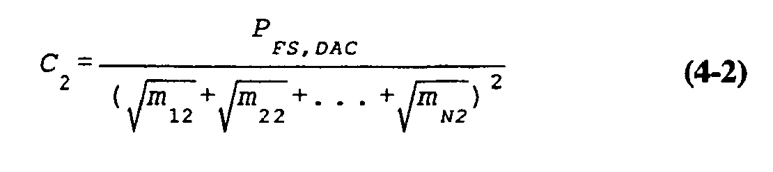
- C 2 P FS , DAC m 12 + m 22 + ⁇ + m N ⁇ 2 2
- C N P FS , DAC m 1 ⁇ N + m 2 ⁇ N + ⁇ + m NN 2
- the Radio Control Unit 450 determines the amount of gain required of the analog power control module 460 to adjust the power level of the individual carriers in the analog domain so that the absolute output power of the carriers is P k,out , where k represents carriers 1...N. Accordingly, the analog gain is calculated in step 520 in accordance with equation (5) shown below, where the analog gain of the analog power control module 460 is G ana , P k,out is the required absolute output power of a particular carrier, C k is the power level of the corresponding carrier in the digital domain, and where G ana , P k,out and C k are in decibels. For simplicity of description, G ana has been described as the gain of power control module 460.
- G ana can represent the total gain in the power control transmitter including the gain in the amplifier and any diminution of power caused by filters and upconverters in the analog section of the transmitter.
- G ana P k , out - C k
- step 525 the power level of each individual carrier is adjusted. Further in accordance with step 525 and as illustrated in figure 4 , once C 1 ...C N have been calculated using equations (4-1) through (4-3) above, the Radio Control Unit 450 sets the gain of DPC 1 ...DPC N so that the output of multipliers Multi 1 ...Multi N have a power level equal to C 1 ...C N. According to equation (3), the in-phase sum of the carrier power levels C 1 ...C N will be equal to the DAC full scale level P FS,DAC . In step 530 the analog power level of a particular carrier P k,out is adjusted using the calculated analog gain G ana . Although steps 525 and 530 in figure 5 are illustrated as occurring sequentially in time, one skilled in the art will recognize that steps 525 and 530 can occur simultaneously.
- Figure 6 illustrates an exemplary multicarrier transmitter where two of the eight carriers are active; the full scale output power of the DAC is 1 milliwatt; the output power of carrier f 2 is 1 Watt; and the output power of carrier f 8 is 0.1 Watts.
- the gain of the Digital Power Control modules DPC 2 and DPC 8 are set such that the power levels of their output signals C 2 and C 8 are .577 mW and .057 mW, respectively.
- the analog gain can be calculated using the eighth carrier frequency f 8 .
- Figure 7 is a graph of the amplitude versus frequency of the two active carriers, f 2 and f 8 , described in the exemplary embodiment above.
- the full scale power output of the DAC is equal to 1 milliwatt, or 0 dBm. Since there are two active carriers, C max would be set at 6 dB, i.e., 20*log 10 (2), below the DAC full scale level.
- the power level of the second carrier is -2.4 dBm and the power of the eighth carrier is -12.4 dBm. Accordingly, using the multicarrier transmitter as described above, results in the power level of the second carrier being approximately 3.6 dB above the C max power level. In contrast, the prior multicarrier transmitters would limit the power levels of the carriers to C max , which would result in a lower signal-to-noise ratio for the carriers.
- the multipliers, multi 1 ...multi N will be used to multiply the baseband data streams by a corresponding spreading code.
- the signals can be combined by the summer and forwarded to the DAC 120.
- digital power control modules DPC 1 ...DPC N adjust the power of the baseband data streams so that the sum of the baseband data streams is equal to the full scale range of the DAC.
- a scrambling code may (optionally) be applied to the summed signal and then forwarded to the analog power control module 460 to adjust the signal power to the correct level required for the receiving mobile stations.
Landscapes
- Engineering & Computer Science (AREA)
- Signal Processing (AREA)
- Computer Networks & Wireless Communication (AREA)
- Transmitters (AREA)
- Mobile Radio Communication Systems (AREA)
Description
- The present invention relates to the field of radio telecommunications, including cellular telecommunications, and more specifically, to maximizing the signal-to-noise ratio in multicarrier transmitters by controlling the power level of each of the carriers entering a digital-to-analog converter and by controlling overall power gain of the analog portion of the transmitter.
- In conventional cellular systems, a base station is allocated a predetermined number of frequency channels for communication with mobile stations. In the base station a separate transmitter is employed for each frequency channel. However, the use of separate transmitters for each frequency channel results in a duplication of parts and an increase in cost due to the additional hardware required. Thereafter, it was realized that the hardware cost per channel could be reduced by using multicarrier transmitters in place of the plurality of single carrier transmitters to transmit a plurality of frequency channels. Since multicarrier transmitters transmit over a broad range of frequencies, they are also sometimes referred to in the art as wideband transmitters. However, for ease of discussion, the transmitters will be referred to herein as multicarrier transmitters.
-
Figure 1 illustrates aconventional multicarrier transmitter 100 which might be used to transmit multiple frequency channels from a base station in a radiocommunication system. Theconventional multicarrier transmitter 100 operates as follows. A number N of baseband frequency data signals BB1....BBN are modulated by modulators Mod1.....ModN, respectively, where the bits associated with each data signal are symbol encoded for transmission, i.e., the modulator generates the corresponding baseband waveform. Each of the modulated data signals is forwarded to a corresponding digital power control module DPC1.....DPCN, where each DPC adjusts the signal power level of the corresponding modulated data signal based on the commands provided by theRadio Control Unit 150. More specifically, the power level of each modulated data signal is adjusted such that the absolute power level of each carrier Pk,out at the transmitter is equal to the amount of power required for the carrier to reach a particular mobile station which is to receive the carrier, where k varies from 1 to N and identifies the corresponding baseband frequency data signals BB1...BBN. - The modulated data signals are then forwarded from the digital power control modules DPC1.....DPCN to multipliers Mult1....MultN, respectively, where each modulated data signal is upconverted to a corresponding carrier frequency. The upconverted signals are then summed by
adder 110. The compound signal produced byadder 110 is then forwarded to the digital-to-analog converter (DAC) 120. The resulting compound analog signal is then passed fromDAC 120 through an analog transmitter chain which includesanalog amplifier 160, upconverter (not shown), and filters (not shown).Analog amplifier 160 then amplifies the compound signal by a fixed gain Gi. For ease of discussion Gi has been described as the gain ofanalog amplifier 160, however, one skilled in the art will recognize that Gi represents the total gain of the analog section of the transmitter, including losses due to filters and upconverters. A more detailed discussion of multicarrier transmitters can be found in "Base-Station Technology Takes Software-Definable Approach" by Richard M. Lober, Wireless System Designs, February 1998. - Multicarrier transmitters are designed to handle a maximum number of simultaneous carriers N. In designing a multicarrier transmitter, care must be taken to ensure that the instantaneous in-phase sum, Psum, of the N carriers does not exceed the full scale range of the DAC, i.e., the value associated with the greatest digital code that can be converted into an analog value. Psum can be calculated using equation (1) below, where CN represents the power of a specific user, N, in a specific time slot on a specific carrier frequency. Normally, CN is equal to the peak power within the specific
time slot. 
- If the instantaneous sum of the N carriers exceeds the full scale range of the DAC, the DAC will clip the analog signal, i.e., prevent the analog signal from exceeding the amplitude corresponding to the full scale range of the DAC, which will affect the quality of the transmitted signal. However, one skilled in the art will recognize that in practical applications, a system might tolerate a power level which exceeds the DAC's full scale range by a small amount for short periods of time without suffering a decrease in system performance.
- In a multicarrier transmitter with N carriers, the abovementioned "clipping" of the analog signal can be avoided by setting the full scale range of the DAC to 20*log(N) dB above the maximum allowed peak power level of any
individual carrier 1...N, since the full scale range set 20*log(N) dB above the maximum power level of any individual carrier represents the greatest power level attainable by the sum of the N carriers. - In
figure 2 , the maximum power level associated with each of the N carriers, during a given time slot in a TDMA based system, is Cmax. Accordingly, the full scale range of the DAC is set to 20*log(N) dB above Cmax. When the output noise of the DAC is dominated by quantization noise, the DAC noise floor level relative to the DAC full scale range, is constant for a given DAC resolution and sampling frequency. If all carriers are operating at maximum power, the signal-to-noise ratio for each individual carrier is at its greatest level. - Unlike
figure 2, figure 3 illustrates a time slot where the N carriers have different power levels and not all of the N carriers are active. Assuming the DAC full scale range infigure 3 is the same as the DAC full scale range infigure 2 , the noise floor levels offigures 2 and 3 will also be the same. Since the power levels of the N carriers infigure 3 are less than the power levels of the N carriers infigure 2 , while the noise floor level infigures 2 and 3 is the same, the signal-to-noise ratio for each of the individual carriers infigure 3 will be lower than for the corresponding individual carriers infigure 2 . - Accordingly, it would be desirable to maximize the signal-to-noise ratio for each carrier and time slot. Further, it would be desirable to maximize the signal-to-noise ratio for each individual carrier in a multicarrier transmitter when less than the maximum number of carriers are used and/or when not all carriers are operating at the maximum power level. In addition, it would be desirable to maximize the signal-to-noise ratio of each individual carrier in the multicarrier transmitter without the instantaneous sum of all the carriers exceeding the DAC's full scale range.
- The power level of individual carriers is adjusted in the digital domain, by a command from a radio control unit, such that Psum is equal to the full scale range of the DAC, or such that Psum exceeds the full scale range of the DAC, though not enough to cause intolerable distortion to the signal. The radio control unit also commands an analog power control module to adjust the power level of all carriers simultaneously such that the transmitted actual absolute output power level of each carrier is set to the correct level for a corresponding mobile station to receive an acceptable signal.
- It is an object of the present invention to improve the signal-to-noise ratio of a multicarrier signal which passes through a DAC.
- It is also an object of the present invention to maximize the utilization of a DAC in a multicarrier transmitter system, thereby reducing the implementation cost of the transmitter chain in a radio base station.
- It is a further object of the present invention to maximize the signal-to-noise ratio of each individual carrier in a multicarrier transmitter, thereby improving end user quality of service for all users.
- The object of the present invention is solved by a multicarrier transmitter according to
claim 1, and by a method for maximizing, in a multicarrier transmitter, a signal-to-noise ratio of each of a plurality of individual carriers according to claim 5. - The present invention will now be described with reference to the accompanying drawings in which:
-
Figure 1 illustrates a conventional multicarrier transmitter; -
Figure 2 illustrates N carriers in one time slot at the maximum power level; -
Figure 3 illustrates a time slot where the N carriers are at different power levels and not all N carriers are active; -
Figure 4 illustrates an exemplary multicarrier transmitter for maximizing the signal-to-noise ratio; -
Figure 5 illustrates an exemplary method for power control; -
Figure 6 illustrates power control of a multicarrier transmitter according to an exemplary embodiment of the present invention; and -
Figure 7 illustrates a time slot where two carriers are active and one carrier's power level exceeds Cmax. - In the following description, for purposes of explanation and not limitation, specific details are set forth, such as particular circuits, circuit components, and techniques, in order to provide a thorough understanding of the present invention. However, it will be apparent to one skilled in the art that the present invention may be practiced in other embodiments that depart from these specific details. In other instances, detailed descriptions of well-known methods, devices, and circuits are omitted so as not to obscure the description of the present invention.
- The exemplary radio communication systems discussed herein are described as using the time division multiple access (TDMA) protocol, in which communication between the base station and the mobile terminals is performed over a number of time slots. However, those skilled in the art will appreciate that the concepts disclosed herein find use in other access methods, including, but not limited to, frequency division multiple access (FDMA), code division multiple access (CDMA), or some hybrid of any of the above protocols. Likewise, some of the exemplary embodiments provide illustrative examples relating to the GSM system, however, the techniques described herein are equally applicable to radio base stations in any system.
-
Figure 4 illustrates amulticarrier transmitter 400 according to exemplary embodiments of the present invention. Similar tomulticarrier transmitter 100 offigure 1 , each of a number of N baseband frequency data signals BB1...BBN are forwarded to a corresponding modulator Mod1...ModN. The modulated baseband signals BB1...BBN are then forwarded to the digital power control modules DPC1...DPCN. TheRadio Control Unit 450 individually sets the gain of each digital power control module DPC1...DPCN, such that Psum is equal to the full scale range of theDAC 120, PFS,DAC. - The signals generated by the digital power control modules DPC1...DPCN are forwarded to multipliers Multi1...MultiN where the signals are upconverted to a corresponding carrier frequency. The upconverted signals are then summed by
adder 110. The resultant compound signal is converted from digital to analog byDAC 120. The analog signal is forwarded to an analogpower control module 460 which is controlled by an analog power control table stored in theRadio Control Unit 450. Although analogpower control module 460 is illustrated as a single element infigure 4 , the functionality of the analogpower control module 460 may be distributed over the analog transmitter chain, i.e., amplifiers, filters and upconverters, in order to minimize the effect on the noise figure. - In order to correctly adjust the absolute power level at the transmitter, Pk,out, for the carrier signals, the power level of the carrier signals are all adjusted by the same amount by the analog
power control module 460. In order to adjust the gain of each digital power control module and the gain of the analogpower control module 460, theRadio Control Unit 450 knows the required power level of each carrier at the output of the transmitter Pk,out, i.e., the amount of transmit power required to provide a corresponding mobile station with an acceptable signal. Since the full scale range of the DAC is determined at the time of installation of the DAC in the multicarrier transmitter, the full scale range PFS,DAC of theDAC 120 and the corresponding code can be programmed into theRadio Control Unit 450. -
Figure 5 is a flow chart illustrating an exemplary method for maximizing the signal-to-noise ratio of each carrier using the multicarrier transmitter illustrated infigure 4 . Accordingly, instep 505, a vector is formed using the output power levels associated with each carrier in a given time slot, e.g., P= [P1,out P2,out P3,out ... PN,out]. Instep 510, using vector P, a matrix M is created where the elements are the ratios of all actual absolute power levels for the time slot.
carrier 2 is not active (P2,out=0) then both the second row and the second column of the matrix are set to zero. - In
step 515, the power levels C1...CN associated with the active carriers are calculated. The power levels C1...CN correspond to the power levels of the respective carriers at the DAC input. Given the number of carriers possible and the power requirements of the carriers and assuming that the DAC full scale range cannot be exceeded, the largest signal-to-noise ratio for each carrier and the sum of the carriers occurs when Psum equals the DAC full scale range, as illustrated in equation (3) below.
- Rearranging equation (3) above, each carrier power level C1...CN can be calculated using the following equations, wherein only active carriers are calculated in order to avoid division by zero:


- In
step 520 theRadio Control Unit 450 determines the amount of gain required of the analogpower control module 460 to adjust the power level of the individual carriers in the analog domain so that the absolute output power of the carriers is Pk,out, where k representscarriers 1...N. Accordingly, the analog gain is calculated instep 520 in accordance with equation (5) shown below, where the analog gain of the analogpower control module 460 is Gana, Pk,out is the required absolute output power of a particular carrier, Ck is the power level of the corresponding carrier in the digital domain, and where Gana, Pk,out and Ck are in decibels. For simplicity of description, Gana has been described as the gain ofpower control module 460. However, one skilled in the art will recognize that Gana can represent the total gain in the power control transmitter including the gain in the amplifier and any diminution of power caused by filters and upconverters in the analog section of the transmitter.
- In
step 525 the power level of each individual carrier is adjusted. Further in accordance withstep 525 and as illustrated infigure 4 , once C1...CN have been calculated using equations (4-1) through (4-3) above, theRadio Control Unit 450 sets the gain of DPC1...DPCN so that the output of multipliers Multi1...MultiN have a power level equal to C1...CN. According to equation (3), the in-phase sum of the carrier power levels C1...CN will be equal to the DAC full scale level PFS,DAC. Instep 530 the analog power level of a particular carrier Pk,out is adjusted using the calculated analog gain Gana. Althoughsteps figure 5 are illustrated as occurring sequentially in time, one skilled in the art will recognize thatsteps -
Figure 6 illustrates an exemplary multicarrier transmitter where two of the eight carriers are active; the full scale output power of the DAC is 1 milliwatt; the output power of carrier f2 is 1 Watt; and the output power of carrier f8 is 0.1 Watts. In accordance withstep 505, the output power vector is P=[0 1 0 0 0 0 0 0.1]. Using the output power vector, the matrix M created according to step 510 becomes:
- Since f2 and f8 are the only carriers, the power levels C2 and C8 are calculated according to step 515:


- Referring now to
figure 6 , the gain of the Digital Power Control modules DPC2 and DPC8 are set such that the power levels of their output signals C2 and C8 are .577 mW and .057 mW, respectively. - The analog gain is calculated according to step 525 using the transmit power level and digital gain for the second carrier frequency f2. Accordingly, P2,out and C2 are converted from Watts to decibels, (i.e., P2,out=1 Watt=10*log1000=30 dBm, and C2=1/1.732 milliWatt=-2.4 dBm). In accordance with equation (5), the analog gain Gana is equal to 32.4 dB, i.e., Gana=30-(-2.4)=32.4 dB. Alternatively, the analog gain can be calculated using the eighth carrier frequency f8. Accordingly, P8,out and C8 are converted from Watts to decibels, (i.e., P8,out=0.1 Watt=10*log100=20 dBm, and C8=1/17.32 milliWatt=-12.4 dBm). In accordance with equation (5), the analog gain Gana is equal to 32.4 dB, i.e., Gana=20-(-12.4)=32.4 dB. Therefore, the
Radio Control Unit 450 sets the gain of the analogpower control module 460 in accordance with the analog gain calculated in accordance with equation (5). -
Figure 7 is a graph of the amplitude versus frequency of the two active carriers, f2 and f8, described in the exemplary embodiment above. As stated above, the full scale power output of the DAC is equal to 1 milliwatt, or 0 dBm. Since there are two active carriers, Cmax would be set at 6 dB, i.e., 20*log10(2), below the DAC full scale level. Further, as stated above, the power level of the second carrier is -2.4 dBm and the power of the eighth carrier is -12.4 dBm. Accordingly, using the multicarrier transmitter as described above, results in the power level of the second carrier being approximately 3.6 dB above the Cmax power level. In contrast, the prior multicarrier transmitters would limit the power levels of the carriers to Cmax, which would result in a lower signal-to-noise ratio for the carriers. - Although the exemplary embodiments described above relate to a TDMA embodiment, one skilled in the art can see that the present invention is equally applicable in a CDMA embodiment. For instance, referring now to
figure 4 , the multipliers, multi1...multiN will be used to multiply the baseband data streams by a corresponding spreading code. The signals can be combined by the summer and forwarded to theDAC 120. Similar to the TDMA embodiment described above, in order to maximize the signal-to-noise ratio of each individual carrier and the sum of the carriers, digital power control modules DPC1...DPCN adjust the power of the baseband data streams so that the sum of the baseband data streams is equal to the full scale range of the DAC. Once the summed signal has been converted into analog, a scrambling code may (optionally) be applied to the summed signal and then forwarded to the analogpower control module 460 to adjust the signal power to the correct level required for the receiving mobile stations. - The present invention has been described by way of exemplary embodiments to which the invention is not limited. Modifications and changes will occur to those skilled in the art without departing from the scope of the invention as defined in the appended claims.
Claims (8)
- A multicarrier transmitter comprising:a plurality of digital power control modules (DPC1, ..., DPCN);a digital-to-analog converter (120);an analog power control module (460);a radio control unit (450) for individually adjusting the gain of each of said plurality of digital power control modules (DPC1, ..., DPCN) such that the square of the sum of the square roots of power levels (C1, ..., CN) associated with the output of each of said digital power control modules corresponding to active carriers is equal to a full scale range (PFS,DAC) of said digital-to-analog converter (120),characterized in that
the radio control unit (450) is further adapted for:- determining each of the power levels (C1, C2, ..., CN) associated with the outputs of said digital power control modules (DPC1, ..., DPCN) corresponding to the active carriers based on a ratio of the full scale range (PFS,DAC) of said digital-to-analog converter (120) and the square of the sum of the square roots of the ratios (m11...mN1, m12...mN2, ..., mN1...mNN) of output power levels (P1, P2, ..., PN) of individual carrier signals at an output of the analog power control module (460) and the respective output power level (P1; P2; ...; PN), corresponding to the respective active carrier, at the output of the analog power control module (460);- calculating a gain (Gana) of said analog power control module as the difference between a predetermined power level of a particular active carrier (Pk,out) and the respective power level of the power levels (C1, C2, ..., CN) associated with the output of said digital power control modules (DPC1, ..., DPCN) corresponding to active carriers; and;- setting the calculated gain (Gana) such that the power levels (P1, P2, ..., PN) of the individual carrier signals at the output of said analog power control module are equal to the predetermined power level (Pk,out). - The multicarrier transmitter of claim 1, wherein said predetermined power level is a power level for which a mobile station corresponding to one of said carrier signals receives a signal of acceptable quality.
- The multicarrier transmitter of claim 1, further comprising:a plurality of modulators (mod1, ..., modN) for modulating a plurality of baseband data streams (BB1data, ..., BBNdata) and providing said modulated data streams to said plurality of digital control modules (DPC1, ..., DPCN);a plurality of multipliers (multi1, ..., multiN) for upconverting signals from said digital power control modules (DPC1, ..., DPCN) to a plurality of corresponding carrier frequencies (f1, ..., fN); andan adder (110) for summing said plurality of upconverted signals and providing said summed signals to said digital-to-analog converter (120).
- The multicarrier transmitter of claim 1, further comprising:a plurality of modulators (mod1, ..., modN) for modulating a plurality of baseband data streams (BB1data, ..., BBNdata) and providing said modulated data streams to said plurality of digital control modules (DPC1, ..., DPCN);a plurality of multipliers (multi1, ..., multiN) for multiplying the baseband data streams (BB1data, ..., BBNdata) from said digital power control modules (DPC1, ..., DPCN) by a spreading code; andan adder (110) for summing said plurality of spreaded baseband data streams and providing said summed signals to said digital-to-analog converter (120).
- A method for maximizing, in a multicarrier transmitter having a plurality of digital power control modules (DPC1, ..., DPCN), an digital-analog converter (120), and an analog power control module (460), a signal-to-noise ratio of each of a plurality of individual carriers, the method comprising the step of:individually adjusting a gain of each of the plurality of digital power control modules (DPC1, ..., DPCN) such that the square of the sum of the square roots of power levels (C1, ..., CN) associated with an output of each of said digital power control modules corresponding to active carriers is equal to a full scale range (PFS,DAC) of said digital-to-analog converter (120),characterized in that the method further comprises the steps of:- determining each of the power levels (C1, C2, ..., CN) associated with the outputs of said digital power control modules (DPC1, ..., DPCN) corresponding to the active carriers based on a ratio of the full scale range (PFS,DAC) of said digital-to-analog converter (120) and the square of the sum of the square roots of the ratios (m11...mN1, m12...mN2, ..., mN1...mNN) of output power levels (P1, P2, ..., PN) of individual carrier signals at an output of the analog power control module (460) and the respective output power level (P1; P2; ...; PN), corresponding to the respective active carrier, at the output of the analog power control module (460);- calculating a gain (Gana) of said analog power control module as the difference between a predetermined power level of a particular active carrier (Pk,out) and the respective power level of the power levels (C1, C2, ..., CN) associated with the output of said digital power control modules (DPC1, ..., DPCN) corresponding to active carriers; and;- setting the calculated gain (Gana) such that the power levels (P1, P2, ..., PN) of the individual carrier signals at the output of said analog power control module are equal to the predetermined power level (Pk,out).
- The method of claim 5, wherein said predetermined power level is a power level which a mobile station corresponding to one of said carrier signals receives a signal of acceptable quality.
- The method of claim 5, further comprising:modulating a plurality of baseband data streams (BB1data, ..., BBNdata) and providing said modulated data streams to said plurality of digital control modules (DPC1, ..., DPCN);upconverting signals from said digital power control modules (DPC1, ..., DPCN) to a plurality of corresponding carrier frequencies (f1, ..., fN); andsumming said plurality of upconverted signals and providing said summed signals to said digital-to-analog converter (120).
- The method of claim 5, further comprising:modulating a plurality of baseband data streams (BB1data, ..., BBNdata) and providing said modulated data streams to said plurality of digital control modules (DPC1, ..., DPCN);multiplying the baseband data streams (BB1data, ..., BBNdata) from said digital power control modules (DPC1, ..., DPCN) by a spreading code; andsumming said plurality of spreaded baseband data streams and providing said summed signals to said digital-to-analog converter (120).
Applications Claiming Priority (3)
| Application Number | Priority Date | Filing Date | Title |
|---|---|---|---|
| US349717 | 1995-01-25 | ||
| US09/349,717 US6570929B1 (en) | 1999-07-08 | 1999-07-08 | Power control scheme for maximizing carrier signal-to-noise ratio in multicarrier transmitters |
| PCT/SE2000/001388 WO2001005111A1 (en) | 1999-07-08 | 2000-06-29 | Power control scheme for maximizing carrier signal-to-noise ratio in multicarrier transmitters |
Publications (2)
| Publication Number | Publication Date |
|---|---|
| EP1195034A1 EP1195034A1 (en) | 2002-04-10 |
| EP1195034B1 true EP1195034B1 (en) | 2008-07-09 |
Family
ID=23373650
Family Applications (1)
| Application Number | Title | Priority Date | Filing Date |
|---|---|---|---|
| EP00946678A Expired - Lifetime EP1195034B1 (en) | 1999-07-08 | 2000-06-29 | Power control scheme for maximizing carrier signal-to-noise ratio in multicarrier transmitters |
Country Status (7)
| Country | Link |
|---|---|
| US (1) | US6570929B1 (en) |
| EP (1) | EP1195034B1 (en) |
| CN (1) | CN1197317C (en) |
| AU (1) | AU6039900A (en) |
| DE (1) | DE60039427D1 (en) |
| ES (1) | ES2307520T3 (en) |
| WO (1) | WO2001005111A1 (en) |
Cited By (1)
| Publication number | Priority date | Publication date | Assignee | Title |
|---|---|---|---|---|
| CN101651513B (en) * | 2008-08-14 | 2012-11-21 | 联芯科技有限公司 | Method and device for processing received signals of wireless communication system terminals |
Families Citing this family (26)
| Publication number | Priority date | Publication date | Assignee | Title |
|---|---|---|---|---|
| AU8730698A (en) * | 1998-06-29 | 2000-01-17 | Nokia Networks Oy | Power control in a multi-carrier radio transmitter |
| US6694148B1 (en) * | 1999-07-26 | 2004-02-17 | Telefonaktiebolaget Lm Ericsson (Publ) | Transmit power control for MCPA-equipped based stations |
| CN1147177C (en) * | 2000-09-26 | 2004-04-21 | 华为技术有限公司 | Method and apparatus for raising carrier output power of wide band multi-carrier base station |
| US7336726B2 (en) * | 2001-02-27 | 2008-02-26 | Huawei Technologies Co., Ltd. | Apparatus and method for power control in digital mobile communication system broadband multi-carrier base station |
| CN100334826C (en) * | 2001-04-17 | 2007-08-29 | 诺基亚公司 | Method for determining different carrier gains, radio transmitter and radio transmitter module |
| ES2283922T3 (en) * | 2001-04-17 | 2007-11-01 | Nokia Corporation | METHODS TO DETERMINE THE PROFITS OF DIFFERENT CARRIERS, RADIOCOMMUNICATION TRANSMISSION UNITS AND MODULES FOR SUCH UNITS. |
| US6862456B2 (en) * | 2002-03-01 | 2005-03-01 | Cognio, Inc. | Systems and methods for improving range for multicast wireless communication |
| US6785520B2 (en) * | 2002-03-01 | 2004-08-31 | Cognio, Inc. | System and method for antenna diversity using equal power joint maximal ratio combining |
| US6687492B1 (en) * | 2002-03-01 | 2004-02-03 | Cognio, Inc. | System and method for antenna diversity using joint maximal ratio combining |
| AU2003219882A1 (en) * | 2002-03-01 | 2003-09-16 | Cognio, Inc. | System and method for joint maximal ratio combining |
| EP2224609B1 (en) * | 2002-03-21 | 2011-08-24 | IPR Licensing Inc. | Improving the efficiency of power amplifiers in devices using transmit beamforming |
| US6871049B2 (en) * | 2002-03-21 | 2005-03-22 | Cognio, Inc. | Improving the efficiency of power amplifiers in devices using transmit beamforming |
| US7194022B2 (en) * | 2002-06-07 | 2007-03-20 | Nokia Corporation | Method and system having capacity-dependent baseband gain and coverage-capacity swapping in a multi-carrier base station transmitters |
| EP1983651B1 (en) * | 2002-07-30 | 2014-11-05 | IPR Licensing, Inc. | Device for multiple-input multiple output (MIMO) radio communication |
| CN100483967C (en) * | 2002-12-31 | 2009-04-29 | 中国科学技术大学 | Transmitter and receiver capable of controlling peak power |
| US7099678B2 (en) * | 2003-04-10 | 2006-08-29 | Ipr Licensing, Inc. | System and method for transmit weight computation for vector beamforming radio communication |
| US20050009477A1 (en) * | 2003-07-10 | 2005-01-13 | Terayon Communications System, Inc., A Delaware Corporation | System and method for an upconverter for stacked intermediate frequency carriers |
| JP4356392B2 (en) * | 2003-08-07 | 2009-11-04 | パナソニック株式会社 | Communication device |
| US20050201180A1 (en) * | 2004-03-05 | 2005-09-15 | Qualcomm Incorporated | System and methods for back-off and clipping control in wireless communication systems |
| KR100628741B1 (en) | 2004-11-25 | 2006-09-29 | 엘지노텔 주식회사 | Apparatus and method for digital combine multi carrier transmitter in mobile communication system |
| US7907671B2 (en) * | 2004-12-03 | 2011-03-15 | Motorola Mobility, Inc. | Method and system for scaling a multi-channel signal |
| CN101778064B (en) * | 2009-01-13 | 2013-05-22 | 财团法人工业技术研究院 | Transmitter for processing peak to average power ratio and method thereof |
| US9674800B2 (en) * | 2009-06-18 | 2017-06-06 | Qualcomm Incorporated | Power scaling for multi-carrier high-speed uplink packet access |
| EP2403302B1 (en) * | 2010-06-29 | 2017-01-04 | Lg Electronics Inc. | User equipment apparatus for transmitting a plurality of signals simultaneously using at least two wireless communication schemes and method thereof |
| US9215120B2 (en) | 2011-12-21 | 2015-12-15 | Telefonaktiebolaget L M Ericsson (Publ) | Multi-band crest factor reduction |
| ES2706431T3 (en) * | 2012-05-03 | 2019-03-28 | Ericsson Telefon Ab L M | Transmitting apparatus and radio communication method |
Family Cites Families (9)
| Publication number | Priority date | Publication date | Assignee | Title |
|---|---|---|---|---|
| US5384547A (en) | 1993-08-02 | 1995-01-24 | Motorola, Inc. | Apparatus and method for attenuating a multicarrier input signal of a linear device |
| EP0719001A1 (en) | 1994-12-22 | 1996-06-26 | ALCATEL BELL Naamloze Vennootschap | DMT modulator |
| US5528199A (en) * | 1994-12-30 | 1996-06-18 | At&T Corp. | Closed-loop frequency control of an oscillator circuit |
| KR0155818B1 (en) | 1995-04-29 | 1998-11-16 | 김광호 | Power distribution method and apparatus in multi-carrier transmitting system |
| US5745846A (en) | 1995-08-07 | 1998-04-28 | Lucent Technologies, Inc. | Channelized apparatus for equalizing carrier powers of multicarrier signal |
| JPH09130245A (en) * | 1995-11-06 | 1997-05-16 | Sony Corp | Gain varying circuit |
| US5894498A (en) | 1997-02-26 | 1999-04-13 | Motorola, Inc. | Method and apparatus for analyzing a composite carrier signal |
| US5987307A (en) * | 1998-10-09 | 1999-11-16 | Denso Corporation | Power control in wireless radio tranceivers |
| US6256502B1 (en) * | 1998-12-23 | 2001-07-03 | Nortel Networks Limited | Wideband multicarrier power control for a cellular PCS basestation tranmitter |
-
1999
- 1999-07-08 US US09/349,717 patent/US6570929B1/en not_active Expired - Lifetime
-
2000
- 2000-06-29 WO PCT/SE2000/001388 patent/WO2001005111A1/en active Application Filing
- 2000-06-29 ES ES00946678T patent/ES2307520T3/en not_active Expired - Lifetime
- 2000-06-29 EP EP00946678A patent/EP1195034B1/en not_active Expired - Lifetime
- 2000-06-29 CN CNB008100756A patent/CN1197317C/en not_active Expired - Fee Related
- 2000-06-29 AU AU60399/00A patent/AU6039900A/en not_active Abandoned
- 2000-06-29 DE DE60039427T patent/DE60039427D1/en not_active Expired - Lifetime
Cited By (1)
| Publication number | Priority date | Publication date | Assignee | Title |
|---|---|---|---|---|
| CN101651513B (en) * | 2008-08-14 | 2012-11-21 | 联芯科技有限公司 | Method and device for processing received signals of wireless communication system terminals |
Also Published As
| Publication number | Publication date |
|---|---|
| CN1197317C (en) | 2005-04-13 |
| ES2307520T3 (en) | 2008-12-01 |
| WO2001005111A1 (en) | 2001-01-18 |
| US6570929B1 (en) | 2003-05-27 |
| AU6039900A (en) | 2001-01-30 |
| EP1195034A1 (en) | 2002-04-10 |
| DE60039427D1 (en) | 2008-08-21 |
| CN1360781A (en) | 2002-07-24 |
Similar Documents
| Publication | Publication Date | Title |
|---|---|---|
| EP1195034B1 (en) | Power control scheme for maximizing carrier signal-to-noise ratio in multicarrier transmitters | |
| US6694148B1 (en) | Transmit power control for MCPA-equipped based stations | |
| EP1388937B1 (en) | Adaptive RF amplifier prelimiter | |
| US5708681A (en) | Hybrid analog/digital method and apparatus for controlling the transmission power level of a radio transceiver | |
| EP3270558B1 (en) | System and apparatus for post filtering peak power reduction in multi-carrier communications systems | |
| EP1502362B1 (en) | System and method for eliminating signal zero crossings in single and multiple channel communication systems | |
| US7340224B2 (en) | Devices for reducing the dynamic range of signals in transmitters of communication systems | |
| US8995565B2 (en) | Distortion control device and method | |
| EP1157481B1 (en) | Cdma signal transmission control | |
| EP1330041B1 (en) | A method and an apparatus for improving the carriers' output power of a broadband multi-carrier base-station | |
| JP2001145147A (en) | System and method for controlling total overload | |
| US20100150126A1 (en) | Method for adjusting transmitter output power | |
| EP1339248B1 (en) | Method and device of gain equalization based on wideband multi-carrier base-station | |
| US6996080B1 (en) | Chip-synchronous CDMA multiplexer and method resulting in constant envelope signals | |
| US7062289B2 (en) | Method and apparatus of multi-carrier power control of base station in broad-band digital mobile communication system | |
| US20050197066A1 (en) | Non-linear distortion compensation circuit for multi-carrier transmission | |
| US7336726B2 (en) | Apparatus and method for power control in digital mobile communication system broadband multi-carrier base station | |
| EP1224745A1 (en) | Transmit power control for mcpa-equipped base stations | |
| ZA200306451B (en) | The apparatus and method for power control in digital mobile communication system broadband multi-carrier base station. | |
| KR100201294B1 (en) | Method and circuit of channel combining in cdma system | |
| ZA200306447B (en) | Method and apparatus of multi-carrier power control of base station in broad-band digital mobile communication system. | |
| KR20050063185A (en) | Par improving method in multi-fa transmitting system |
Legal Events
| Date | Code | Title | Description |
|---|---|---|---|
| PUAI | Public reference made under article 153(3) epc to a published international application that has entered the european phase |
Free format text: ORIGINAL CODE: 0009012 |
|
| 17P | Request for examination filed |
Effective date: 20020130 |
|
| AK | Designated contracting states |
Kind code of ref document: A1 Designated state(s): AT BE CH CY DE DK ES FI FR GB GR IE IT LI LU MC NL PT SE |
|
| AX | Request for extension of the european patent |
Free format text: AL;LT;LV;MK;RO;SI |
|
| RAP1 | Party data changed (applicant data changed or rights of an application transferred) |
Owner name: TELEFONAKTIEBOLAGET LM ERICSSON (PUBL) |
|
| RBV | Designated contracting states (corrected) |
Designated state(s): DE ES |
|
| 17Q | First examination report despatched |
Effective date: 20061002 |
|
| GRAP | Despatch of communication of intention to grant a patent |
Free format text: ORIGINAL CODE: EPIDOSNIGR1 |
|
| GRAS | Grant fee paid |
Free format text: ORIGINAL CODE: EPIDOSNIGR3 |
|
| GRAA | (expected) grant |
Free format text: ORIGINAL CODE: 0009210 |
|
| AK | Designated contracting states |
Kind code of ref document: B1 Designated state(s): DE ES |
|
| REF | Corresponds to: |
Ref document number: 60039427 Country of ref document: DE Date of ref document: 20080821 Kind code of ref document: P |
|
| REG | Reference to a national code |
Ref country code: ES Ref legal event code: FG2A Ref document number: 2307520 Country of ref document: ES Kind code of ref document: T3 |
|
| PLBE | No opposition filed within time limit |
Free format text: ORIGINAL CODE: 0009261 |
|
| STAA | Information on the status of an ep patent application or granted ep patent |
Free format text: STATUS: NO OPPOSITION FILED WITHIN TIME LIMIT |
|
| 26N | No opposition filed |
Effective date: 20090414 |
|
| PGFP | Annual fee paid to national office [announced via postgrant information from national office to epo] |
Ref country code: ES Payment date: 20140626 Year of fee payment: 15 |
|
| PGFP | Annual fee paid to national office [announced via postgrant information from national office to epo] |
Ref country code: DE Payment date: 20140627 Year of fee payment: 15 |
|
| REG | Reference to a national code |
Ref country code: DE Ref legal event code: R119 Ref document number: 60039427 Country of ref document: DE |
|
| PG25 | Lapsed in a contracting state [announced via postgrant information from national office to epo] |
Ref country code: DE Free format text: LAPSE BECAUSE OF NON-PAYMENT OF DUE FEES Effective date: 20160101 |
|
| REG | Reference to a national code |
Ref country code: ES Ref legal event code: FD2A Effective date: 20160729 |
|
| PG25 | Lapsed in a contracting state [announced via postgrant information from national office to epo] |
Ref country code: ES Free format text: LAPSE BECAUSE OF NON-PAYMENT OF DUE FEES Effective date: 20150630 |