EP1193859A2 - Noise reduction technique in current steered chopper stabilized amplifier - Google Patents
Noise reduction technique in current steered chopper stabilized amplifier Download PDFInfo
- Publication number
- EP1193859A2 EP1193859A2 EP01308383A EP01308383A EP1193859A2 EP 1193859 A2 EP1193859 A2 EP 1193859A2 EP 01308383 A EP01308383 A EP 01308383A EP 01308383 A EP01308383 A EP 01308383A EP 1193859 A2 EP1193859 A2 EP 1193859A2
- Authority
- EP
- European Patent Office
- Prior art keywords
- amplifier
- signal
- circuit
- clock
- output
- Prior art date
- Legal status (The legal status is an assumption and is not a legal conclusion. Google has not performed a legal analysis and makes no representation as to the accuracy of the status listed.)
- Withdrawn
Links
Images




Classifications
-
- H—ELECTRICITY
- H03—ELECTRONIC CIRCUITRY
- H03F—AMPLIFIERS
- H03F3/00—Amplifiers with only discharge tubes or only semiconductor devices as amplifying elements
- H03F3/38—DC amplifiers with modulator at input and demodulator at output; Modulators or demodulators specially adapted for use in such amplifiers
-
- H—ELECTRICITY
- H03—ELECTRONIC CIRCUITRY
- H03F—AMPLIFIERS
- H03F3/00—Amplifiers with only discharge tubes or only semiconductor devices as amplifying elements
- H03F3/45—Differential amplifiers
- H03F3/45071—Differential amplifiers with semiconductor devices only
- H03F3/45076—Differential amplifiers with semiconductor devices only characterised by the way of implementation of the active amplifying circuit in the differential amplifier
- H03F3/45179—Differential amplifiers with semiconductor devices only characterised by the way of implementation of the active amplifying circuit in the differential amplifier using MOSFET transistors as the active amplifying circuit
- H03F3/45183—Long tailed pairs
- H03F3/45192—Folded cascode stages
-
- H—ELECTRICITY
- H03—ELECTRONIC CIRCUITRY
- H03F—AMPLIFIERS
- H03F3/00—Amplifiers with only discharge tubes or only semiconductor devices as amplifying elements
- H03F3/45—Differential amplifiers
- H03F3/45071—Differential amplifiers with semiconductor devices only
- H03F3/45479—Differential amplifiers with semiconductor devices only characterised by the way of common mode signal rejection
- H03F3/45632—Differential amplifiers with semiconductor devices only characterised by the way of common mode signal rejection in differential amplifiers with FET transistors as the active amplifying circuit
- H03F3/45636—Differential amplifiers with semiconductor devices only characterised by the way of common mode signal rejection in differential amplifiers with FET transistors as the active amplifying circuit by using feedback means
- H03F3/45641—Measuring at the loading circuit of the differential amplifier
- H03F3/4565—Controlling the common source circuit of the differential amplifier
-
- H—ELECTRICITY
- H03—ELECTRONIC CIRCUITRY
- H03F—AMPLIFIERS
- H03F3/00—Amplifiers with only discharge tubes or only semiconductor devices as amplifying elements
- H03F3/45—Differential amplifiers
- H03F3/45071—Differential amplifiers with semiconductor devices only
- H03F3/45479—Differential amplifiers with semiconductor devices only characterised by the way of common mode signal rejection
- H03F3/45632—Differential amplifiers with semiconductor devices only characterised by the way of common mode signal rejection in differential amplifiers with FET transistors as the active amplifying circuit
- H03F3/45695—Differential amplifiers with semiconductor devices only characterised by the way of common mode signal rejection in differential amplifiers with FET transistors as the active amplifying circuit by using feedforward means
- H03F3/4573—Measuring at the common source circuit of the differential amplifier
- H03F3/45739—Controlling the loading circuit of the differential amplifier
-
- H—ELECTRICITY
- H03—ELECTRONIC CIRCUITRY
- H03F—AMPLIFIERS
- H03F3/00—Amplifiers with only discharge tubes or only semiconductor devices as amplifying elements
- H03F3/45—Differential amplifiers
- H03F3/45071—Differential amplifiers with semiconductor devices only
- H03F3/45479—Differential amplifiers with semiconductor devices only characterised by the way of common mode signal rejection
- H03F3/45632—Differential amplifiers with semiconductor devices only characterised by the way of common mode signal rejection in differential amplifiers with FET transistors as the active amplifying circuit
- H03F3/45744—Differential amplifiers with semiconductor devices only characterised by the way of common mode signal rejection in differential amplifiers with FET transistors as the active amplifying circuit by offset reduction
- H03F3/45775—Differential amplifiers with semiconductor devices only characterised by the way of common mode signal rejection in differential amplifiers with FET transistors as the active amplifying circuit by offset reduction by using cross switches
-
- H—ELECTRICITY
- H03—ELECTRONIC CIRCUITRY
- H03F—AMPLIFIERS
- H03F2203/00—Indexing scheme relating to amplifiers with only discharge tubes or only semiconductor devices as amplifying elements covered by H03F3/00
- H03F2203/45—Indexing scheme relating to differential amplifiers
- H03F2203/45356—Indexing scheme relating to differential amplifiers the AAC comprising one or more op-amps, e.g. IC-blocks
-
- H—ELECTRICITY
- H03—ELECTRONIC CIRCUITRY
- H03F—AMPLIFIERS
- H03F2203/00—Indexing scheme relating to amplifiers with only discharge tubes or only semiconductor devices as amplifying elements covered by H03F3/00
- H03F2203/45—Indexing scheme relating to differential amplifiers
- H03F2203/45631—Indexing scheme relating to differential amplifiers the LC comprising one or more capacitors, e.g. coupling capacitors
-
- H—ELECTRICITY
- H03—ELECTRONIC CIRCUITRY
- H03F—AMPLIFIERS
- H03F2203/00—Indexing scheme relating to amplifiers with only discharge tubes or only semiconductor devices as amplifying elements covered by H03F3/00
- H03F2203/45—Indexing scheme relating to differential amplifiers
- H03F2203/45651—Indexing scheme relating to differential amplifiers the LC comprising two cascode current sources
-
- H—ELECTRICITY
- H03—ELECTRONIC CIRCUITRY
- H03F—AMPLIFIERS
- H03F2203/00—Indexing scheme relating to amplifiers with only discharge tubes or only semiconductor devices as amplifying elements covered by H03F3/00
- H03F2203/45—Indexing scheme relating to differential amplifiers
- H03F2203/45682—Indexing scheme relating to differential amplifiers the LC comprising one or more op-amps
Definitions
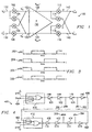
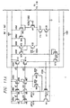
- Switches 102, 108 for example would be closed when the phii signal 202 is high and its complement, phiib 402, is low.
- the switches 102, 108 would be opened, on the other hand, when the phii signal 202 is low and its complement, phiib 402, is high.
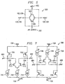
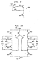
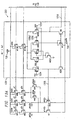
- Vout- 142 To output a low signal on Vout- 142 would similarly require current passing through three transistors (e.g., through M9, M11, and M2 or M10, M12, and M8).
- M9, M11, and M2 or M10, M12, and M8 the closest the voltage of the V out + signal 140 could reach to gnda 692 would be: gnda +V DS (M10) + V DS (M12) + V DS (M4) .
- the closest the V out . signal 142 could be to the Vdda reference voltage would be: Vdda-V DS (M14) -V DS (M16) -V DS (M7) .
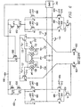
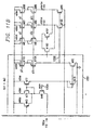
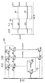
- the other amplifiers (An2', Ap1', Ap2') operate in a similar fashion with their associated transistor amplifiers, and the operation of the amplifiers will be coordinated to such that the output signals will be appropriated steered in unison with the input chopping.
- Bypass paths include hard-wired connections, RF connections, acoustic connections, or optical connections, and may include other elements interposed in the bypass paths.
- a given amplifier stage can include one or more than one sub-stages and/or one or more amplifying elements.
- a connection between amplifier stages or between other elements can include additional amplifiers or filtering elements, and therefore connections between elements recited in this application shall be inclusive of connections having additional elements interposed between such elements.
Landscapes
- Engineering & Computer Science (AREA)
- Power Engineering (AREA)
- Amplifiers (AREA)
Abstract
Description
| U.S. Patent No. | Filing Date |
| 6,002,299 | December 14, 1999 |
Claims (25)
- An amplifier circuit comprising:a) a first amplifier sub-circuit having a signal input and a clock input, said signal input operable to receive an input signal, and said clock input operable to receive a clock signal, said first amplifier sub-circuit operable to generate first and second output signals, each output signal including a clock component based on said clock signal input;b) a second amplifier sub-circuit having an input connected to said first output signal, a feedback path connected to said input signal, and an output, said second amplifier sub-circuit operable to be turned off when said clock component is in a first condition and to collectively form a gain-boosted cascode amplifier with said first sub-circuit to provide an amplified signal at its output when said clock component is in a second condition; andc) a third amplifier sub-circuit having an input connected to said second output signal, a feedback path connected to said input signal, and an output, said third amplifier sub-circuit operable to be turned off when said clock component is in said second condition and to collectively form a gain-boosted cascode amplifier with said first subcircuit to provide an amplified signal at its output, when said clock component is in said first condition
- The amplifier circuit of claim 1 wherein said first amplifier sub-circuit is an operational amplifier.
- The amplifier circuit of claim 1 wherein each of said second and third amplifier sub-circuits are transistor circuits.
- The amplifier circuit of claim 3 wherein each of said transistor circuits comprises multiple transistors.
- The amplifier circuit of claim 3 wherein each of said transistor circuits consists of single transistors.
- The amplifier circuit of claim 1 wherein said at least one transistor amplifier comprises more than one transistor.
- The amplifier circuit of claim 1 wherein said clock component comprises non-overlapping clock signals on said first and second outputs, whereby a first clock signal is provided on said first output and a second clock signal is provided on said second output, and wherein said clock signals are approximately non-overlapping.
- The amplifier circuit of claim 1 wherein the voltages of said clock component is such that when said second and third amplifier sub-circuits are substantially not saturated, whereby said second and third amplifiers are operating in a substantially in linear mode.
- The amplifier of claim 1 wherein said amplifier is connected to a positive and a negative supply rail, and wherein said second and third sub-circuits each comprise at least one transistor amplifier and wherein said clock component oscillates over a voltage range that lies substantially within said positive and negative supply rails.
- The amplifier circuit of claim 9 wherein the range of said output voltage of said second and third sub-circuits includes an output voltage that is removed from one of said positive and negative supply rails by less than three VDS voltage drops of a MOS transistor.
- The amplifier circuit of claim 1 wherein said clock component is derived from said chopper clock signal.
- A chopper stabilized amplifier comprising:a) first and second differential voltage inputs;b) an input chopper switch having a chopper clock signal input, having inputs connected to said first and second differential voltage inputs, and providing first and second signal path outputs, said input chopper switch operable during one phase of said chopper clock signal to connect said first differential voltage input to said first signal path output and said second differential voltage input to said second signal path output, and during the other phase of said chopper clock signal to connect said second differential voltage input to said first signal path output and said first differential voltage input to said second signal path output;c) at least one current-steering amplifier connected to each of said first and second signal path outputs, each of said current-steering amplifiers comprising:i) a first amplifier sub-circuit having a signal input for receiving the signal from the respective first or second signal path output and a clock input for receiving a clock signal based on said chopper clock, said first amplifier sub-circuit operable to generate first and second output signals, each output signal including a clock component based on said clock signal input;ii) a second amplifier sub-circuit having a signal input connected to said first output signal from said first amplifier sub-circuit, a feedback path connected to said signal input, and an output, said second amplifier sub-circuit operable to be turned off when said clock component is in a first condition and to collectively form a cascode amplifier with said first sub-circuit to provide an amplified signal at its output when said clock component is in a second condition; andiii) a third amplifier sub-circuit having an input connected to said second output signal from said first amplifier sub-circuit, a feedback path connected to said signal input, and an output, said third amplifier sub-circuit operable to be turned off when said clock component is in said second condition and to collectively form a cascode amplifier with said first sub-circuit to provide an amplified signal at its output when said clock component is in said first condition.
- The amplifier of claim 12 wherein said current-steering amplifier is connected to a positive and a negative supply rail, and wherein said second and third sub-circuits each comprises at least one transistor amplifier and wherein said clock component oscillates over a voltage range that lies substantially within said positive and negative supply rails.
- The amplifier circuit of claim 13 wherein the range of said output voltage of said second and third sub-circuits includes an output voltage that is removed from one of said positive and negative supply rails by less than three VDS voltage drops of a MOS transistor.
- The amplifier circuit of claim 12 wherein further circuitry is interposed between said input chopper switch and said at least one current-steering amplifier.
- The amplifier circuit of claim 12 wherein said clock component is derived from said chopper clock signal.
- The amplifier circuit of claim 12 wherein said second and third sub-circuits each comprise at least one transistor amplifier.
- The amplifier circuit of claim 17 wherein said at least one transistor amplifier comprises multiple transistors.
- The amplifier circuit of claim 17 wherein said at least one transistor amplifier consists of a single transistor.
- A method of amplifying a signal comprising:a) receiving Vin+ and Vin- differential signal inputs;b) providing an amplifier circuit having a first signal path and a second signal path, each signal path operable to amplify separately one of said differential signal inputs;c) providing input steering switches to alternatively switch which of said differential signal inputs is directed to said first signal path and which is directed to said second signal path;d) providing Vout+ and Vout- differential signal outputs; ande) providing a combination switching/amplifying circuit for amplifying each said differential signal inputs and for simultaneously switching said differential signal inputs to alternating ones of said Vout+ and Vout- differential signal outputs.
- The method of claim 20 and further comprising providing a clock signal which oscillates about a reference voltage, said reference voltage being less than a positive rail voltage provided to said amplifier circuit and greater than a negative rail voltage provided to said amplifier circuit.
- The method of claim 21 and further comprising modulating said combination amplifying/switching circuit with said analog clock signal.
- The method of claim 22 wherein said combination switching/amplifying circuit is a sub-amplifier circuit having at least one transistor amplifier whose base is driven by a gain-boosting amplifier that outputs a signal comprising a component which is an amplified signal based on the differential voltage between the Vin+ and Vin- signal inputs and a component which is said analog clock signal.
- The method of claim 21 wherein said analog clock signal is derived from said chopper clock signal.
- The method of claim 20 wherein said Vout+ and Vout- signals are capable of being driven to within three VDS voltage drops of a MOS transistor from the power supply voltages provided to the amplifier.
Applications Claiming Priority (2)
| Application Number | Priority Date | Filing Date | Title |
|---|---|---|---|
| US09/678,166 US6307430B1 (en) | 2000-10-02 | 2000-10-02 | Noise reduction technique in chopper stabilized amplifier |
| US678166 | 2000-10-02 |
Publications (2)
| Publication Number | Publication Date |
|---|---|
| EP1193859A2 true EP1193859A2 (en) | 2002-04-03 |
| EP1193859A3 EP1193859A3 (en) | 2004-06-30 |
Family
ID=24721669
Family Applications (1)
| Application Number | Title | Priority Date | Filing Date |
|---|---|---|---|
| EP01308383A Withdrawn EP1193859A3 (en) | 2000-10-02 | 2001-10-01 | Noise reduction technique in current steered chopper stabilized amplifier |
Country Status (2)
| Country | Link |
|---|---|
| US (1) | US6307430B1 (en) |
| EP (1) | EP1193859A3 (en) |
Families Citing this family (15)
| Publication number | Priority date | Publication date | Assignee | Title |
|---|---|---|---|---|
| CN1575542A (en) * | 2001-10-25 | 2005-02-02 | 皇家飞利浦电子股份有限公司 | Operational amplifier with chopped input transistor pair |
| US6636098B1 (en) * | 2001-12-05 | 2003-10-21 | Rambus Inc. | Differential integrator and related circuitry |
| US7091771B2 (en) * | 2003-01-21 | 2006-08-15 | Cirrus Logic, Inc. | Segmented chopping amplifier |
| US6961385B2 (en) * | 2003-01-21 | 2005-11-01 | Cirrus Logic, Inc. | Signal processing system with baseband noise modulation chopper circuit timing to reduce noise |
| SE0301927D0 (en) * | 2003-06-30 | 2003-06-30 | Infineon Technologies Ag | Bi-polar RNP chopper |
| US7295061B1 (en) | 2004-09-02 | 2007-11-13 | Marvell International Ltd. | Fully integrated programmable gain chopper amplifier with self DC offset suppression |
| US7202746B1 (en) | 2004-12-14 | 2007-04-10 | Cirrus Logic, Inc. | Multiple-stage operational amplifier and methods and systems utilizing the same |
| US7262654B2 (en) * | 2005-01-14 | 2007-08-28 | Cirrus Logic, Inc. | Circuits and methods for minimizing chopping artifacts at the output of a chopper-stabilized operational amplifier |
| US7170338B1 (en) | 2005-03-24 | 2007-01-30 | Cirrus Logic, Inc. | Chopper stabilization circuits and methods |
| US7310016B2 (en) * | 2005-07-13 | 2007-12-18 | Texas Instruments Incorporated | Chopper-stabilized operational amplifier and method |
| US7816988B2 (en) * | 2006-02-03 | 2010-10-19 | Honglei Wu | Amplifier |
| US8099073B1 (en) * | 2007-05-22 | 2012-01-17 | Marvell International Ltd. | Noise reduction in amplifier circuitry using single-sideband chopper stabilization |
| EP2109214B1 (en) * | 2008-04-10 | 2014-06-04 | ams AG | Amplifier arrangement and method for signal amplification |
| KR20140108363A (en) * | 2013-02-25 | 2014-09-11 | 삼성전자주식회사 | Operational amplifier and apparatus for sensing touch including operational amplifier |
| CN108494370B (en) * | 2018-05-31 | 2023-12-29 | 福州大学 | Chopper stabilized instrumentation amplifier |
Family Cites Families (35)
| Publication number | Priority date | Publication date | Assignee | Title |
|---|---|---|---|---|
| US3638130A (en) * | 1970-06-08 | 1972-01-25 | Honeywell Inc | High-speed amplifier for driving an inductive load |
| US3991730A (en) | 1975-01-30 | 1976-11-16 | Chrysler Corporation | Noise immune reset circuit for resetting the integrator of an electronic engine spark timing controller |
| US3989961A (en) | 1975-06-16 | 1976-11-02 | The Boeing Company | Bidirectional reset integrator converter |
| JPS6244597Y2 (en) | 1979-12-05 | 1987-11-26 | ||
| US4318613A (en) | 1980-04-10 | 1982-03-09 | The Nuarc Company, Inc. | Universal light integrator/timer for photographic equipment |
| US4384257A (en) | 1981-05-29 | 1983-05-17 | Nola William M | Storage stabilized integrator |
| US4509037A (en) | 1981-06-12 | 1985-04-02 | Gould Inc. | Enhanced delta modulation encoder |
| US4559634A (en) | 1982-08-16 | 1985-12-17 | Texas Instruments Incorporated | PSK Modem having dual-integrator voltage controlled oscillator |
| US4502020A (en) | 1983-10-26 | 1985-02-26 | Comlinear Corporation | Settling time reduction in wide-band direct-coupled transistor amplifiers |
| US4559502A (en) | 1984-04-19 | 1985-12-17 | Signetics Corporation | Multi-stage amplifier with capacitive nesting for frequency compensation |
| GB2182219B (en) | 1985-10-24 | 1990-07-04 | Stc Plc | High gain feed back amplifier |
| US4628279A (en) | 1985-12-26 | 1986-12-09 | Comlinear Corporation | Wideband feedback amplifier |
| US4713628A (en) | 1986-10-08 | 1987-12-15 | Comlinear Corporation | Compensation and biasing of wideband amplifiers |
| US4780689A (en) | 1987-07-20 | 1988-10-25 | Comlinear Corporation | Amplifier input circuit |
| US4766367A (en) | 1987-07-20 | 1988-08-23 | Comlinear Corporation | Current mirror with unity gain buffer |
| FR2619974B1 (en) | 1987-08-26 | 1991-10-18 | France Etat | FILTERING QUADRIPOLE WITH SWITCHED CAPACITIES TO LINEARIZE THE PHASE / FREQUENCY RESPONSE OF SAID FILTER |
| US4757275A (en) | 1987-11-20 | 1988-07-12 | Comlinear Corporation | Wideband closed loop amplifier |
| US4808942A (en) | 1988-04-04 | 1989-02-28 | General Electric Company | Continuous mode auto-zero offset amplifier or integrator |
| US4939516B1 (en) | 1988-06-13 | 1993-10-26 | Crystal Semiconductor Corporation | Chopper stabilized delta-sigma analog-to-digital converter |
| US4926178A (en) | 1988-07-13 | 1990-05-15 | Analog Devices, Inc. | Delta modulator with integrator having positive feedback |
| GB8818703D0 (en) | 1988-08-05 | 1988-09-07 | Gen Electric Co Plc | Delta sigma modulator arrangements |
| US4906944A (en) | 1988-08-17 | 1990-03-06 | Rockwell International Corporation | Integrator controlled time compensated clock oscillator |
| US5012244A (en) | 1989-10-27 | 1991-04-30 | Crystal Semiconductor Corporation | Delta-sigma modulator with oscillation detect and reset circuit |
| US5477481A (en) | 1991-02-15 | 1995-12-19 | Crystal Semiconductor Corporation | Switched-capacitor integrator with chopper stabilization performed at the sampling rate |
| US5115202A (en) * | 1991-04-10 | 1992-05-19 | Analog Devices, Inc. | Chopper-stabilized amplifier with spread-spectrum clocking |
| JP2520056B2 (en) | 1991-04-10 | 1996-07-31 | 東光株式会社 | Polarized Leapfrog Filter |
| JPH06164258A (en) | 1992-11-20 | 1994-06-10 | Fuji Xerox Co Ltd | Amplifier circuit with offset cancel circuit |
| US5317277A (en) | 1992-12-08 | 1994-05-31 | Doble Engineering Company | Power amplifying apparatus for supplying A.C. signals having a maximum loop gain at a desired frequency |
| US5635871A (en) | 1992-12-15 | 1997-06-03 | Doble Engineering Company | Low phase error amplifying |
| US5381112A (en) * | 1993-09-22 | 1995-01-10 | Motorola, Inc. | Fully differential line driver circuit having common-mode feedback |
| US5451901A (en) | 1994-07-01 | 1995-09-19 | Cirrus Logic Inc. | Transconductance amplifiers and exponential variable gain amplifiers using the same |
| JPH08279718A (en) | 1995-04-07 | 1996-10-22 | Nec Corp | Offset eliminating amplifier circuit |
| US5789981A (en) * | 1996-04-26 | 1998-08-04 | Analog Devices, Inc. | High-gain operational transconductance amplifier offering improved bandwidth |
| US5847607A (en) * | 1996-12-19 | 1998-12-08 | National Semiconductor Corporation | High speed fully differential operational amplifier with fast settling time for switched capacitor applications |
| US6002299A (en) * | 1997-06-10 | 1999-12-14 | Cirrus Logic, Inc. | High-order multipath operational amplifier with dynamic offset reduction, controlled saturation current limiting, and current feedback for enhanced conditional stability |
-
2000
- 2000-10-02 US US09/678,166 patent/US6307430B1/en not_active Expired - Lifetime
-
2001
- 2001-10-01 EP EP01308383A patent/EP1193859A3/en not_active Withdrawn
Also Published As
| Publication number | Publication date |
|---|---|
| EP1193859A3 (en) | 2004-06-30 |
| US6307430B1 (en) | 2001-10-23 |
Similar Documents
| Publication | Publication Date | Title |
|---|---|---|
| EP1193859A2 (en) | Noise reduction technique in current steered chopper stabilized amplifier | |
| EP1510000B1 (en) | Operational amplifier with independent input offset trim for high and low common mode input voltages | |
| KR100301332B1 (en) | Differential Amplifiers with Rail-to-Rail Common-Mode Ranges | |
| EP0649218B1 (en) | Gain enhancement technique for operational amplifiers | |
| US6529070B1 (en) | Low-voltage, broadband operational amplifier | |
| KR100284024B1 (en) | Low Voltage Seamos Op Amp Circuit and Sample and Hold Circuit With It | |
| KR100620662B1 (en) | Differential ab class amplifier circuit and drive circuit using the same | |
| US8063702B2 (en) | High frequency receiver preamplifier with CMOS rail-to-rail capability | |
| US4887048A (en) | Differential amplifier having extended common mode input voltage range | |
| US6573779B2 (en) | Duty cycle integrator with tracking common mode feedback control | |
| JP4564285B2 (en) | Semiconductor integrated circuit | |
| JPH09509019A (en) | Differential amplifier with high differential impedance and low common mode impedance | |
| EP0685126B1 (en) | Cmos operational amplifier with improved rail-to-rail performance | |
| US7126596B1 (en) | Rail-to-rail amplifier for use in line-inversion LCD grayscale reference generator | |
| JPH07288432A (en) | Continuous -time common mode feedback amplifier | |
| WO2009059185A2 (en) | Differential amplifier system | |
| JP4408715B2 (en) | Driving circuit and processing circuit | |
| JP4605601B2 (en) | Operational amplifier | |
| US5745007A (en) | CMOS differential amplifier having constant transconductance and slew rate | |
| US6208199B1 (en) | Pulse amplifier with low duty cycle errors | |
| US6194966B1 (en) | Cmos class ab operational amplifier operating from a single 1.5v cell | |
| US6781463B2 (en) | Low voltage amplifier | |
| US10270392B1 (en) | Low-power differential amplifier with improved unity gain frequency | |
| JP6338807B1 (en) | Class AB amplifier and operational amplifier | |
| JP2009517975A (en) | Small signal amplifier with large signal output boost stage |
Legal Events
| Date | Code | Title | Description |
|---|---|---|---|
| PUAI | Public reference made under article 153(3) epc to a published international application that has entered the european phase |
Free format text: ORIGINAL CODE: 0009012 |
|
| AK | Designated contracting states |
Kind code of ref document: A2 Designated state(s): AT BE CH CY DE DK ES FI FR GB GR IE IT LI LU MC NL PT SE TR |
|
| AX | Request for extension of the european patent |
Free format text: AL;LT;LV;MK;RO;SI |
|
| RAP1 | Party data changed (applicant data changed or rights of an application transferred) |
Owner name: CIRRUS LOGIC, INC. |
|
| PUAL | Search report despatched |
Free format text: ORIGINAL CODE: 0009013 |
|
| AK | Designated contracting states |
Kind code of ref document: A3 Designated state(s): AT BE CH CY DE DK ES FI FR GB GR IE IT LI LU MC NL PT SE TR |
|
| AX | Request for extension of the european patent |
Extension state: AL LT LV MK RO SI |
|
| 17P | Request for examination filed |
Effective date: 20040609 |
|
| 17Q | First examination report despatched |
Effective date: 20040920 |
|
| AKX | Designation fees paid |
Designated state(s): AT BE CH CY DE DK ES FI FR GB GR IE IT LI LU MC NL PT SE TR |
|
| 17Q | First examination report despatched |
Effective date: 20040920 |
|
| GRAP | Despatch of communication of intention to grant a patent |
Free format text: ORIGINAL CODE: EPIDOSNIGR1 |
|
| STAA | Information on the status of an ep patent application or granted ep patent |
Free format text: STATUS: THE APPLICATION IS DEEMED TO BE WITHDRAWN |
|
| 18D | Application deemed to be withdrawn |
Effective date: 20110726 |