BACKGROUND OF THE INVENTION
This application claims the benefit of a
Japanese Patent Application No.2000-301464 filed
September 29, 2000, in the Japanese Patent Office,
the disclosure of which is hereby incorporated by
reference.
1. Field of the Invention
The present invention generally relates to
rotation control methods and storage apparatuses,
and more particularly to a rotation control method
for controlling rotation of a recording medium such
as an optical disk when recording information on
and/or reproducing information from the recording
medium, and to a storage apparatus which employs
such a rotation control method.
Recording media such as optical disks
employ a zone constant angular velocity (ZCAV)
system or a zone constant linear velocity (ZCLV)
system. When the ZCAV system is employed, it is
possible to obtain a high random access performance
with respect to the recording medium, but a
recording and/or reproducing clock frequency becomes
low. For example, a data transfer rate at an inner
periphery of the optical disk becomes slow. On the
other hand, when the ZCLV system is employed, it is
possible to obtain a high data transfer rate, but
the random access performance with respect to the
recording medium becomes poor because the rotational
speed of the recording medium such as the optical
disk changes upon access thereto.
2. Description of the Related Art
Recently, due to the popular use of the
Internet, there are increased opportunities for
users to download data, such as music and video data,
via a communication line or the like, and to record
the downloaded data in recording media. In such
cases, magnetic disks of a hard disk drive (HDD),
and removable optical disks such as a digital
versatile disk random access memory (DVD-RAM) are
used as the recording media.
In the case of the video data, the size of
one file is relatively large. In addition, the
video data is a continuous data, and it is necessary
to continuously and stably maintain the data
transfer rate over a predetermined value during
recording to or reproduction from the optical disk,
in order not to generate an image distortion such as
frame dropout.
On the other hand, in personal computers
or the like, a disk management area is usually
provided in a portion of the optical disk for the
purposes of managing programs and files.
Accordingly, it becomes necessary to access the disk
management area every time an access is made to the
program or file. For this reason, in a case where
the size of each file is relatively small, the
access to the file and the access to the disk
management area are repeated, to thereby generate a
random access to the optical disk.
Therefore, the required data transfer rate
and the required random access performance differ
depending on the state of use of the recording
medium, such as the kind of data processed, the file
size and the usage of the recording medium.
As a result, there was a problem in that
it is conventionally impossible to appropriately set
the data transfer rate and the random access
performance depending on the state of use of the
recording medium, such as the kind of data processed,
the file size and the usage of the recording medium.
SUMMARY OF THE INVENTION
Accordingly, it is a general object of the
present invention to provide a novel and useful
rotation control method and storage apparatus, in
which the problems described above are eliminated.
Another and more specific object of the
present invention is to provide a rotation control
method and a storage apparatus, which can set an
optimum data transfer rate and an optimum random
access performance depending on the state of use of
the recording medium.
Still another object of the present
invention is to provide a rotation control method
for controlling rotation of a CAV system recording
medium which has a plurality of zones divided in a
radial direction thereof, comprising a detecting
step which detects a state within a memory which
temporarily stores write data to be written on the
recording medium and/or read data read from the
recording medium, and a controlling step which
switches and controls a rotational speed of the
recording medium based on the state detected by the
detecting step, depending on an area which is
accessed of a plurality of areas of the recording
medium dividing the recording medium in the radial
direction thereof. According to the rotation
control method of the present invention, it is
possible to set an optimum data transfer rate and an
optimum random access performance depending on the
state of use of the recording medium. In addition,
by detecting the state of use of the memory, a
rotational speed switching (changing) time becomes
inconspicuous when viewed from a host unit, thereby
making it possible to secure a desired data transfer
rate without deteriorating the data transfer rate
with respect to the host unit.
A further object of the present invention
is to provide a storage apparatus for recording
and/or reproducing information with respect to a CAV
system recording medium which has a plurality of
zones divided in a radial direction thereof,
comprising a memory which temporarily stores write
data to be written on the recording medium and/or
read data read from the recording medium, a detector
detecting a state within the memory, and a
controller switching and controlling a rotational
speed of the recording medium based on the state
detected by the detector, depending on an area which
is accessed of a plurality of areas of the recording
medium dividing the recording medium in the radial
direction thereof. According to the storage
apparatus of the present invention, it is possible
to set an optimum data transfer rate and an optimum
random access performance depending on the state of
use of the recording medium. In addition, by
detecting the state of use of the memory, a
rotational speed switching (changing) time becomes
inconspicuous when viewed from a host unit, thereby
making it possible to secure a desired data transfer
rate without deteriorating the data transfer rate
with respect to the host unit.
Other objects and further features of the
present invention will be apparent from the
following detailed description when read in
conjunction with the accompanying drawings.
BRIEF DESCRIPTION OF THE DRAWINGS
FIG. 1 is a system block diagram showing
the construction of a first embodiment of a storage
apparatus according to the present invention;
FIG. 2 is a cross sectional view showing
the general construction of an enclosure;
FIG. 3 is a diagram showing the
relationships of a zone on an optical disk, a data
transfer rate and a rotational speed of the optical
disk;
FIG. 4 is a diagram showing the
relationships of the data transfer rate and the
rotational speed of the optical disk with respect to
the zone on the optical disk;
FIG. 5 is a flow chart for explaining the
operation of a MPU of the first embodiment;
FIG. 6 is a flow chart for explaining the
operation of the MPU of the first embodiment;
FIG. 7 is a diagram showing the
relationships of the zone on the optical disk, a
recording or reproducing clock frequency and the
rotational speed of the optical disk;
FIG. 8 is a diagram showing the
relationships of the zone on the optical disk, a
recording or reproducing power and the rotational
speed of the optical disk;
FIG. 9 is a flow chart for explaining an
eccentric acceleration information switching
process;
FIG. 10 is a diagram for explaining the
eccentric acceleration information switching
process;
FIG. 11 is a diagram for explaining a
buffer region provided on the optical disk;
FIG. 12 is a diagram showing a
relationship of a physical block address and a
rotational speed for each zone;
FIG. 13 is a flow chart for explaining a
rotational speed control in the first embodiment;
FIG. 14 is a diagram for explaining a
rotational speed increasing process and a read data
flow in the first embodiment;
FIG. 15 is a diagram for explaining the
rotational speed increasing process and a write data
flow in the first embodiment;
FIG. 16 is a flow chart for explaining the
rotational speed control in a second embodiment;
FIG. 17 is a diagram showing read hit
target data and vacant regions of a DRAM;
FIG. 18 is a diagram showing a table for
managing the read hit target data;
FIG. 19 is a flow chart for explaining a
process of investigating an amount of read hit
target data in the DRAM;
FIG. 20 is a diagram for explaining the
rotational speed increasing process and the read hit
target data in the DRAM in the second embodiment;
FIG. 21 is a flow chart for explaining the
rotational speed control in a third embodiment;
FIG. 22 is a flow chart for explaining a
read statistical information updating process;
FIG. 23 is a diagram showing the read hit
target data and the vacant regions of the DRAM;
FIG. 24 is a diagram showing the table for
managing the read hit target data;
FIG. 25 is a flow chart for explaining the
process of investigating the amount of read hit
target data in the DRAM;
FIG. 26 is a diagram for explaining the
rotational speed increasing process and the read
data flow in the third embodiment;
FIG. 27 is a flow chart for explaining the
rotational speed control in a fourth embodiment;
FIG. 28 is a flow chart for explaining a
write statistical information updating process;
FIG. 29 is a diagram showing write data
and vacant regions in the DRAM;
FIG. 30 is a diagram showing a table for
managing the write data;
FIG. 31 is a flow chart for explaining a
process of investigating a vacant capacity in the
DRAM;
FIG. 32 is a diagram for explaining the
rotational speed increasing process and the write
data flow in the fourth embodiment;
FIG. 33 is a flow chart for explaining the
rotational speed control in a fifth embodiment;
FIG. 34 is a diagram for explaining a
continuation of high-speed rotation after the
rotational speed increasing process in the fifth
embodiment;
FIG. 35 is a diagram for explaining the
continuation of high-speed rotation after the
rotational speed increasing process in the fifth
embodiment;
FIG. 36 is a flow chart for explaining the
rotational speed control of a sixth embodiment;
FIG. 37 is a diagram for explaining the
continuation of high-speed rotation after the
rotational speed increasing process in the sixth
embodiment;
FIG. 38 is a diagram for explaining the
continuation of high-speed rotation after the
rotational speed increasing process in the sixth
embodiment;
FIG. 39 is a flow chart for explaining the
rotational speed control in a seventh embodiment;
FIG. 40 is a flow chart for explaining the
rotational speed control in the seventh embodiment;
FIG. 41 is a diagram for explaining a
priority write process at an existing rotational
speed and the rotational speed increasing process in
the seventh embodiment; and
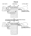
FIG. 42 is a diagram for explaining the
priority write process at the existing rotational
speed and the rotational speed increasing process in
the seventh embodiment.
DESCRIPTION OF THE PREFERRED EMBODIMENTS
A description will be given of embodiments
of a rotation control method according to the
present invention and a storage apparatus according
to the present invention, by referring to the
drawings.
First, a description will be given of a
first embodiment of the storage apparatus according
to the present invention, by referring to FIGS. 1
and 2. FIG. 1 is a system block diagram showing the
construction of this first embodiment of the storage
apparatus. In this first embodiment of the storage
apparatus, the present invention is applied to an
optical disk unit. In addition, this first
embodiment of the storage apparatus employs a first
embodiment of the rotation control method according
to the present invention.
As shown in FIG. 1, the optical disk unit
generally includes a control unit 10 and an
enclosure 11. The control unit 10 includes a
microprocessor unit (MPU) 12 which generally
controls the operation of the optical disk unit, an
interface 17 which exchanges commands and data
between a host unit (not shown), an optical disk
controller (ODC) 14 which carries out processes
required to read and write data with respect to an
optical disk (not shown), a digital signal processor
(DSP) 16, and a memory 18. The memory 18 is used in
common by the MPU 12, the ODC 14 and the interface
14, and for example, includes a dynamic random
access memory (DRAM), a nonvolatile memory which
stores control programs and flag information, or the
like. A crystal oscillator 101 is coupled to the
MPU 12.
The ODC 14 includes a formatter 14-1 and
an error correction code (ECC) processor 14-2. At
the time of a write access, the formatter 14-1
divides NRZ write data into sector units of the
optical disk and generates a recording format, and
the ECC processor 14-2 generates and adds an ECC
with respect to sector write data units and also
generates and adds if necessary a cyclic redundancy
check (CRC) code. Further, the ECC processor 14-2
converts the sector data with the encoded ECC into a
1-7 run length limited (RLL) code, for example.
At the time of a read access, a reverse
conversion of the 1-7 RLL is carried out with
respect to the sector data, and after carrying out
the CRC, the error detection and error correction
using the ECC are carried out in the ECC processor
14-2. Further, the NRZ data in sector units are
connected in the formatter 14-1 so as to transfer a
NRZ read data stream to the host unit.
A write large scale integrated (LSI)
circuit 20 is provided with respect to the ODC 14.
This write LSI circuit 20 includes a write modulator
21 and a laser diode control circuit 22. A control
output of the laser diode control circuit 22 is
supplied to a laser diode unit 30 which is provided
in an optical unit of the enclosure 11. The laser
diode unit 30 integrally includes a laser diode 30-1
and a monitoring detector 30-2. The write modulator
21 converts the write data into the data format of
the pit position modulation (PPM) recording (or mark
recording) or, a pulse width modulation (PWM)
recording (or edge recording).
When recording and reproducing data with
respect to the optical disk using the laser diode
unit 30, this embodiment uses a writable magneto-optical
(MO) cartridge medium employing the PWM
recording which records the data in correspondence
with the existence of mark edges on the optical disk.
In addition, the recording format used by the
optical disk is a 1.3 GB format using magnetic super
resolution (MSR) and the ZCAV system. When the
optical disk is loaded into the optical disk unit,
an identification (ID) portion of the optical disk
is first read, so as to recognize the type (storage
capacity and the like) of the optical disk in the
MPU 12 based on pit intervals of the ID portion.
The MPU 12 notifies the recognition result
indicating the type of optical disk to the ODC 14.
A read LSI circuit 24 is provided as a
read system with respect to the ODC 14. A read
demodulator 25 and a frequency synthesizer 26 are
provided in the read LSI circuit 24. An ID/MO
detector 32 of the enclosure 11 detects a laser beam
emitted from the laser diode 30-1 and returned via
the optical disk, and a detection signal from this
ID/MO detector 32 is input as an ID signal and a MO
signal to the read LSI circuit 24 via a head
amplifier 34.
The read demodulator 25 of the read LSI
circuit 24 includes the functions of circuits such
as an automatic gain control (AGC) circuit, a filter
and a sector mark detection circuit. Hence, the
read demodulator 25 generates a read clock and read
data from the input ID signal and MO signal, and
demodulates the PWM data back into the original NRZ
data. In addition, since the ZCAV system is
employed, the MPU 12 controls a setting of a
frequency dividing ratio with respect to the
frequency synthesizer 26 of the read LSI circuit 24
in order to generate a clock frequency in
correspondence with the zone.
The frequency synthesizer 26 is a phase
locked loop (PLL) circuit having a programmable
frequency divider, and generates as a read clock a
reproducing reference clock having a predetermined
specific frequency depending on the zone position on
the optical disk. In other words, the frequency
synthesizer 26 is formed by the PLL circuit having
the programmable frequency divider, and in a normal
mode, generates the recording and/or reproducing
reference clock having a frequency fo based on fo =
(m/n)fi according to a frequency dividing ratio m/n
which is set by the MPU 12 depending on a zone
number.
A denominator n of the frequency dividing
ratio m/n is a specific value depending on the type
of optical disk. In addition, a numerator m of the
frequency dividing ratio m/n is a value which
changes depending on the zone position on the
optical disk, and table information of the values
corresponding to the zone numbers are prepared in
advance with respect to each type of optical disk.
Moreover, fi denotes a recording and/or reproducing
reference clock frequency generated outside the
frequency synthesizer 26.
The read data demodulated in the read LSI
circuit 24 is supplied to the read system of the ODC
14, and after carrying out the reverse conversion of
the 1-7 RLL, the CRC and the ECC processes are
carried out by the encoding function of the ECC
processor 14-2 so as to restore the original NRZ
data. Next, the formatter 14-1 connects and
converts the NRZ sector data into the NRZ data
stream, and this NRZ read data stream is transferred
to the host unit via the memory 18 and the interface
17.
A detection signal from a temperature
sensor 36 provided in the enclosure 11 is supplied
with respect to the MPU 12 via the DSP 16. Based on
an environmental temperature within the optical disk
unit detected by the temperature sensor 36, the MPU
12 controls the light emission powers for the read,
write and erase in the laser diode control circuit
22.
The MPU 12 controls a spindle motor 40
provided in the enclosure 11 via the DSP 16 and a
driver 38. In this embodiment, since the ZCAV
system is employed as the recording format of the
optical disk, the spindle motor 40 is rotated at a
constant speed of 3637 rpm, for example.
In addition, the MPU 12 controls an
electromagnet 44 provided in the enclosure 11 via
the DSP 16 and a driver 42. The electromagnet 44 is
arranged on a side opposite to the side of the
optical disk on which the laser beam is irradiated
within the optical disk unit which is loaded with
this optical disk. This electromagnet 44 supplies
an external magnetic field on the optical disk at
the time of the recording and erasure. In the case
of the optical disk having the 1.3 GB format
employing the MSR, the electromagnet 44 also
supplies the external magnetic field on the optical
disk at the time of the MSR reproduction.
The DSP 16 is provided with a servo
function for positioning the laser beam from the
laser diode 30-1 with respect to the optical disk,
and functions as a seek controller and an on-track
controller which enable the laser beam to seek a
target track and to be positioned on the target
track. The seek control and the on-track control
may be carried out simultaneously in parallel with
the write access or the read access of the MPU 12
with respect to a host command.
In order to realize the servo function of
the DSP 16, a focus error signal (FES) detector 45
is provided in the optical unit of the enclosure 11
so as to detect the laser beam emitted from the
laser diode 30-1 and returned via the optical disk.
A FES detection circuit 46 generates a FES E1 from a
detection signal received from the FES detector 45,
and inputs this FES E1 to the DSP 16.
A tracking error signal (TES) detector 47
is also provided in the optical unit of the
enclosure 11 so as to detect the laser beam emitted
from the laser diode 30-1 and returned via the
optical disk. A TES detection circuit 48 generates
a TES E2 from a detection signal received from the
TES detector 47, and inputs this TES E2 to the DSP
16. The TES E2 is also input to a track zero
crossing (TZC) detection circuit 50, and this TZC
detection circuit 50 generates a TZC signal E3 which
is input to the DSP 16.
A lens position sensor 54 is provided in
the enclosure 11. This lens position sensor 54
detects a position of an object lens through which
the laser beam is irradiated on the optical disk. A
lens position detection signal (LPOS) E4 from the
lens position sensor 54 is input to the DSP 16. The
DSP 16 controls and drives a focus actuator 60, a
lens actuator 64 and a voice coil motor (VCM) 68 via
corresponding drivers 58, 62 and 66, so as to
control the position of a beam spot formed by the
laser beam on the optical disk.
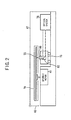
FIG. 2 is a cross sectional view showing
the general construction of the enclosure 11. As
shown in FIG. 2, the spindle motor 40 is provided
within a housing 67. By inserting a MO cartridge 70
into the housing 67 from the side of an inlet door
69, an optical disk (MO disk) 72 accommodated within
the MO cartridge 70 engages a rotary shaft of the
spindle motor 40, thereby loading the optical disk
72 with respect to the optical disk unit.
A carriage 76 is provided below the loaded
optical disk 72 within the MO cartridge 70. This
carriage 76 is freely movable in a direction which
traverses tracks on the optical disk 72 when driven
by the VCM 64. An objective lens 80 is mounted on
the carriage 76. The laser beam emitted from the
laser diode 30-1 which is provided within a fixed
optical system 78 is reflected by a mirror 82, and
is irradiated on the recording surface of the
optical disk 72 via the objective lens 80, thereby
forming a beam spot on the recording surface.
The movement of the objective lens 80
along an optical axis is controlled by the focus
actuator 60 of the enclosure shown in FIG. 1. In
addition, the objective lens 80 is movable in a
radial direction which traverses the tracks on the
optical disk 72 by the lens actuator 64, within a
range of several tens of tracks. The position of
the objective lens 80 mounted on the carriage 76 is
detected by the lens position sensor 54 shown in FIG.
1. The lens position sensor 54 outputs the lens
position detection signal E4 which takes a value
zero at a neutral position where the optical axis of
the objective lens 80 is perpendicular to the
recording surface of the optical disk 72, and has a
magnitude and a polarity depending on the amount the
optical axis of the objective lens 80 moves towards
the inner or outer peripheral side of the optical
disk 72.
Since the ZCAV system is employed, the
optical disk 72 is divided into a plurality of zones
in the radial direction thereof. In the normal mode,
the optical disk 72 is rotated at a constant
rotational speed by the spindle motor 40, and the
recording and/or reproducing reference clock has the
same frequency within each of the zones. In
addition, the frequency of the recording and/or
reproducing clock is set higher for the outer
peripheral side of the optical disk 72 than the
inner peripheral side of the optical disk 72. In
this embodiment, this optical disk 72 is divided
into a number of areas less than or equal to the
number of zones, from the outer peripheral side to
the inner peripheral side of the optical disk 72.
Furthermore, the spindle motor 40 is controlled so
that the rotational speed of the optical disk 72
becomes higher towards the inner peripheral side for
every area. In other words, in a high-speed mode,
the rotational speed of the optical disk 72 is
switched in each area by a number of times such that
undesirable effects on the random access performance
are suppressed, and the recording and/or reproducing
clock and the recording and/or reproducing power in
the laser diode control circuit 22 are switched
accordingly. Hence, in the normal mode, a high
random access performance is obtained because the
optical disk 72 which employs the ZCAV system is
used in conformance with the ZCAV system. On the
other hand, in the high-speed mode, a high data
transfer rate is obtained during the recording
and/or reproduction with respect to the optical disk
72 because the optical disk 72 which employs the
ZCAV system is used in conformance with a kind of
ZCLV system.
In the normal mode, the rotational speed
of the optical disk 72 is controlled to be constant.
On the other hand, the rotational speed of the
optical disk 72 is switched and controlled in a
plurality of stages.
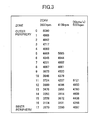
FIG. 3 is a diagram showing the
relationships of the zone on the optical disk 72,
the data transfer rate and the rotational speed of
the optical disk 72. For the sake of convenience,
FIG. 3 shows a case where one area is made up of
zone units, but as described above, the relationship
between the area and the zone is not limited to that
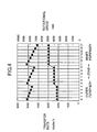
shown in FIG. 3. In addition, FIG. 4 is a diagram
showing the relationships of the data transfer rate
and the rotational speed of the optical disk 72 with
respect to the zone on the optical disk 72. In FIG.
4, a rectangular mark indicates the data transfer
rate, and a triangular mark indicates the rotational
speed of the optical disk 72. FIGS. 3 and 4 show
the relationships for a case where the optical disk
72 has a storage capacity of 1.3 GB and the
rotational speed of the optical disk 72 can be
switched among three rotational speeds in the high-speed
mode. Furthermore, it is assumed for the sake
of convenience that a zone 0 is located on the outer
peripheral side of the optical disk 72 and a zone 17
is located on the inner peripheral side of the
optical disk 72.
In the high-speed mode, in the zone 17
located at the innermost peripheral side of the
optical disk 72, for example, the rotational speed
of the optical disk 72 is switched to 5001 rpm, and
the data transfer rate is 4097 Kbyte/s. In the
normal mode, the rotational speed is 3637 rpm and
the data transfer rate is 2979 Kbyte/s in the zone
17, and it may be seen that the data transfer rate
is improved in the high-speed mode. Accordingly, it
is possible to obtain a desired data transfer rate
on the order of approximately 3700 to 3800 Kbyte/s.
In this embodiment, the upper limit of the data
transfer rate is restricted to 5121 Kbyte/s or less
due to a limit frequency of the circuit, and for
this reason, it is not possible to operate at the
rotational speed of 5001 rpm in the zones 0 through
10 located on the outer peripheral side of the zone
11. However, the rotational speeds and the data
transfer rates which are switched are of course not
limited to those shown in FIGS. 3 and 4, and the
number of switchable rotational speeds is not
limited to three.
In the case of a continuous data such as
video and music data amounting to a large amount of
data, the video or music stops during the recording
and/or reproduction to generate an image distortion,
frame dropout and the like, unless the data transfer
rate is maintained over a reference value. The data
transfer rate during the recording and/or
reproduction of a digital video (DV) format is 3700
to 3800 Kbyte/s, and the image and sound becomes
discontinuous if the data transfer rate is lower
than this data transfer rate range. In the case
shown in FIG. 3, the data transfer rate is lower
than 3700 Kbyte/s on the inner peripheral side of
the zones 12 through 17 when the rotational speed is
3637 rpm, and it may be seen that this data transfer
rate is not suited for the recording and/or
reproduction of the continuous data such as the
video and music data amounting to the large amount
of data. Hence, the rotational speed is switched to
5001 rpm, so that the data transfer rate of 3700 to
3800 Kbyte/s is guaranteed from the inner peripheral
side to the outer peripheral side of the optical
disk 72. Because of the limit frequency of the
circuit, it is not possible to set the rotational
speed to 5001 rpm or higher at all areas on the
optical disk 72, and for this reason, an area where
the rotational speed is set to 4138 rpm is also
provided on the optical disk 72. In this manner,
the rotational speed of the optical disk 72 is
changed depending on the area, so that the data
transfer rate becomes 3700 to 3800 Kbyte/s or
greater at all areas from the inner peripheral side
to the outer peripheral side of the optical disk 72.
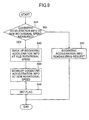
FIGS. 5 and 6 are flow charts for
explaining the operation of the MPU 12 of this
embodiment.
In FIG. 5, a step S1 decides whether or
not a recording or reproducing instruction is issued
from the host unit. If the decision result in the
step S1 is YES, a step S2 decides whether or not a
normal mode, that is, a low-speed rotation fixed
mode of the ZCAV system, is instructed. If the
decision result in the step S2 is YES, a step S3
sets a low-speed rotation request, and the process
advances to a step S21 shown in FIG. 6 which will be
described later.
On the other hand, if the decision result
in the step S2 is NO, a kind of mode of the ZCLV
system is instructed, and thus, a step S4 decides
whether or not the present recording or reproducing
position is located at a position recordable or
reproducible in the high-speed mode, that is,
whether or not the present recording or reproducing
position is located on the inner peripheral side of
a position where a high-speed rotation is possible.
If the decision result in the step S4 is NO, a step
S5 decides whether or not the present recording or
reproducing position is on the outermost peripheral
side of the optical disk 72, that is, in a vicinity
of a leading region of the optical disk 72. If the
decision result in the step S5 is NO, a step S6
initializes an inner access counter within the MPU
12, a step S7 initializes an inner access time
managed within the MPU 12, and the process advances
to the step S3. In addition, if the decision result
in the step S5 is YES, a step S8 decreases a value
of the inner access counter by α, a step S9
increases a value of the inner access time by β,
and the process advances to the step S3.
Therefore, in the leading region of the
optical disk 72, the conditions for judging
continuity of the access is relaxed, so that the
rotational speed increases more easily. Regions for
managing a state of use of the files, such as a FAT
region and a directory region, are provided in the
leading region of the optical disk 72. Even when
the host unit carries out a sequential process with
respect to a region on the inner peripheral side of
the optical disk 72, an access to the leading region
is generated since the directory region is
occasionally updated in order to update or add the
file information. Accordingly, by relaxing the
conditions for judging the continuity of the access,
even if the rotational speed decreases due to the
updating of only the directory information during
the sequential process, the rotational speed
increases before the random access so as to prevent
the random access performance from deteriorating.
If the decision result in the step S4 is
YES, a step S11 decides whether or not the
continuity of the access needs to be judged. The
process advances to a step S15 which will be
described later if the decision result in the step
S11 is NO. ON the other hand, if the decision
result in the step S11 is YES, a step S12 increments
the inner access counter by one, and a step S13
decides whether or not the value of the inner access
counter is greater than or equal to a prescribed
value. The process advances to the step S3 if the
decision result in the step S13 is NO, and the
process advances to a step S14 if the decision
result in the step S13 is YES. The step S14 decides
whether or not a prescribed time has elapsed from a
last outer access which is made in a low-speed mode,
and the process advances to the step S3 if the
decision result in the step S14 is NO. If the
decision result in the step S14 is YES or the
decision result in the step S11 is NO, the step S15
sets a high-speed rotation request for recording or
reproducing in the high-speed mode, and the process
advances to the step S21 shown in FIG. 6.
The prescribed time described above is set
so that the rotational speed of the optical disk 72
which once decreases does not easily increase again,
to thereby prevent deterioration of the random
access performance and the decrease of the data
transfer rate which would otherwise occur if the
rotational speed were frequently switched.
In FIG. 6, the step S21 decides whether or
not the high-speed rotation request exists, and the
process advances to a step S22 if the decision
result in the step S21 is NO. The step S22 decides
whether or not the present mode is the normal mode,
that is, the optical disk 72 is undergoing low-speed
rotation. If the decision result in the step S22 is
YES, a step S23 carries out a seek to a target track
on the optical disk 72, to carry out a recording or
reproduction. If the decision result in the step
S22 is NO, a step S24 sets a low-speed rotation
switching request, and the process advances to a
step S27 which will be described later.
If the decision result in the step S21 is
YES, a step S25 decides whether or not the present
mode is the high-speed mode, that is, the optical
disk 72 is undergoing a high-speed rotation. The
process advances to the step S23 if the decision
result in the step S21 is YES. If the decision
result in the step S25 is NO or after the step S24,
the step S27 turns OFF the tracking servo based on
the TES E2. A step S28 decides whether or not the
high-speed rotation request exists. If the decision
result in the step S28 is NO, a step S29 turns OFF
the focus servo based on the FES E1, and turns OFF
the laser diode 30-1, in order to prevent the data
on the optical disk 72 from being destroyed. If the
decision result in the step S28 is YES or after the
step S29, a step S30 starts switching of the
rotational speed. The switching of the rotational
speed may be carried out based on a table which
indicates the relationships shown in FIG. 3, for
example, by storing the table in the memory 18, for
example.
A step S31 changes eccentric acceleration
information depending on the new rotational speed of
the optical disk 72 after the switching of the
rotational speed. The eccentric acceleration
information is changed by replacing contents
(eccentric acceleration information) of an eccentric
acceleration table within the memory 18, for example,
or by recalculating the eccentric acceleration
information, depending on the new rotational speed.
The eccentric acceleration information relates to
the acceleration which is generated due to the
eccentricity of the optical disk 72, and will be
described later. A step S32 changes various
recording or reproducing parameters which are used
during the recording or reproduction, depending on
the new rotational speed. A step S33 confirms the
stabilized rotation of the optical disk 72. A step
S34 turns ON the laser diode 30-1 if the laser diode
30-1 is OFF. A step S35 turns ON the focus servo if
the focus servo is OFF. In addition, a step S36
turns ON the tracking servo if the tracking servo is
OFF, and the process advances to the step S23.
By the operation described above, it is
possible to carry out a process (1) which switches
and sets between the low-speed rotation fixed mode
and the rotational speed switching mode, and a
process (2) which switches and sets whether or not
to judge the continuity of the access in the
rotational speed switching mode. The process (1)
can be carried out by setting a flag which is used
for the decision in the step S2 shown in FIG. 5. In
addition, the process (2) can be carried out by
setting a flag which is used for the decision in the
step S11 shown in FIG. 5 in a state where the
process (1) sets the rotational speed switching mode.
Methods of setting these flags are not limited to
specific methods. For example, a method which sets
the mode from the host unit, a method which sets the
mode in a nonvolatile memory within the memory 18,
and a method which writes mode setting information
on the optical disk 72 from the host unit and sets
the mode based on the written mode setting
information may be used to set these flags.
The recording or reproducing parameters
set in the step S32 shown in FIG. 6 include the
recording or reproducing clock frequency and the
recording or reproducing power of the laser diode
30-1. FIGS. 7 and 8 are diagrams for explaining the
recording or reproducing parameters which are
changed.
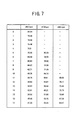
FIG. 7 is a diagram showing the
relationships of the zone on the optical disk 72,
the recording or reproducing clock frequency and the
rotational speed of the optical disk 72. In FIG. ,
the unit of the recording or reproducing clock
frequency is MHz.
FIG. 8 is a diagram showing the
relationships of the zone on the optical disk 72,
the recording or reproducing power and the
rotational speed of the optical disk 72. In FIG. 8,
a rectangular mark indicates a case where the
rotational speed is 3637 rpm, a triangular mark
indicates a case where the rotational speed is 4138
rpm, and a circular mark indicates a case where the
rotational speed is 5001 rpm.
For example, as proposed in a Japanese
Laid-Open Patent Application No.11-73669, a test
write obtains an error quantity of an optimum
recording or reproducing power with respect to a
default recording or reproducing power of a power
default table, so as to optimize the recording or
reproducing power. For this reason, this embodiment
does not need to carry out the test write every time
the rotational speed is switched. In other words,
when the rotational speed is switched, it is only
necessary to switch the power default table
corresponding to each rotational speed, and the
optimum recording or reproducing power at each
rotational speed can be optimized by correcting the
default recording or reproducing power of the
corresponding power default table by the same error
quantity.
Furthermore, this embodiment can minimize
the processing time, because the process of changing
the parameters dependent on the rotational speed of
the optical disk 72, such as the eccentric
acceleration information and the recording or
reproducing parameters, is carried out in parallel
with the process of switching the rotational speed.
FIG. 9 is a flow chart for explaining an
eccentric acceleration information switching process
of the step S31 shown in FIG. 6. In this embodiment,
it is assumed for the sake of convenience that the
eccentric acceleration information switching process
is carried out by the DSP 16 under the control of
the MPU 12. In FIG. 9, a step S41 decides whether
or not the eccentric acceleration information at the
new rotational speed of the optical disk 72 is
already measured in the past. If the decision
result in the step S41 is NO, a step S42 sets an
eccentric acceleration information remeasuring
request, and the process ends. Hence, the eccentric
acceleration information at the new rotational speed
is measured by a known method and is stored in the
eccentric acceleration table. For example, methods
of measuring and learning the eccentric acceleration
information are proposed in a Japanese Laid-Open
Patent Application No.2000-339729.
On the other hand, if the decision result
in the step S41 is YES, a step S43 provides a backup
for the eccentric acceleration information
corresponding to the old rotational speed and stored
in the memory within the DSP 16 or in the memory 18.
A step S44 develops the eccentric acceleration
information corresponding to the new rotational
speed in the memory within the DSP 16 or in the
memory 18. A step S45 sets a flag with respect to
the eccentric acceleration information corresponding
to the old rotational speed, and the process ends.
The eccentric acceleration information
changes when the rotational speed of the optical
disk 72 changes, and thus, it is necessary to obtain
the eccentric acceleration information depending on
the rotational speed. Because it takes time to
measure and store the eccentric acceleration
information, it is desirable not to carry out the
process of remeasuring the eccentric acceleration
information as much as possible when the rotational
speed is switched. Hence, this embodiment decides
whether or not the eccentric acceleration
information corresponding to the new rotational
speed is already measured, and if in the affirmative,
this embodiment merely replaces the contents of the
eccentric acceleration table, so as to minimize the
processing time by omitting the remeasuring process.
FIG. 10 is a diagram for explaining the
eccentric acceleration information switching process
of the step S31 shown in FIG. 6. More particularly,
FIG. 10 is a diagram for explaining a case where the
eccentric acceleration information is switched by
calculation. In FIG. 10, the ordinate indicates the
eccentric acceleration in arbitrary units, and the
abscissa indicates a memory cell number in the
memory within the DSP 16 or in the memory 18. In
addition, a rectangular mark indicates the eccentric
acceleration corresponding to a case where the
rotational speed is 5001 rpm, and a diamond mark
indicates the eccentric acceleration corresponding
to a case where the rotational speed is 3637 rpm.
In the DSP 16, a reference signal
indicating one rotation of the optical disk 72 is
generated based on a signal obtained via the read
LSI circuit 24 and the ODC 14. This reference
signal maintains the relationship with respect to a
position along a circumferential direction of the
optical disk 72 even when the rotational speed of
the optical disk 72 changes. Accordingly, the DSP
16 calculates the eccentric acceleration information
(eccentric acceleration transition) amounting to one
rotation based on the reference signal, and
successively stores the eccentric acceleration
information in the memory cell numbers of the memory
within the DSP 16 or within the memory 18. For the
sake of convenience, FIG. 10 shows a case where the
eccentric acceleration information of the eccentric
acceleration table corresponding to the rotational
speed of 5001 rpm is calculated from the eccentric
acceleration information of the eccentric
acceleration table corresponding to the rotational
speed of 3637 rpm. Accordingly, the eccentric
acceleration in this case becomes (5001/3637)2 times
when the rotational speed of the optical disk 72
changes, and an eccentric acceleration table is
calculated in which the eccentric acceleration
information stored in the memory cell numbers is
multiplied by (5001/3637)2. Furthermore, since the
elapsed time corresponding to one memory cell is
multiplied by (3637/5001), if an updating time of
the memory cells for the case where the rotational
speed is 3637 rpm is denoted by 1, the parameters
are set with respect to the DSP 16 so that the
memory cells are updated 1 x (3637/5001) at a time
for the case where the rotational speed is 5001 rpm.
Therefore, according to this embodiment,
it is possible to an optimum random access
performance or data transfer rate depending on the
needs, by switching the table of the recording or
reproducing parameters, such as the recording or
reproducing clock frequency, the recording or
reproducing power and the eccentric acceleration
information, when the rotational speed of the
optical disk 72 is switched.
FIG. 11 is a diagram for explaining a
buffer region provided on the optical disk 72. As
indicated by a rectangular surrounding mark in FIG.
11, the buffer region may be provided at a boundary
portion of the optical disk 72 between a region
which is accessible in the normal mode and a region
which is accessible in the high-speed mode. In this
case, when an access request to the region which is
accessible in the high-speed mode is generated in
the normal mode, it is detected that the access is
generated with respect to the region located on the
inner peripheral side of the buffer region on the
optical disk 72, and the optical disk 82 is rotated
at the high rotational speed to switch the mode to
the high-speed mode. In other words, the operation
of the MPU 12 in this case is substantially the same
as the operation of the first embodiment, except
that the buffer region is recognized.
When an access request to a certain region
on the outer peripheral side of the optical disk 72
is generated in the high-speed mode, and this
certain region is the buffer region, it is possible
not to immediately switch to the normal mode, but to
switch to the normal mode when an access request to
a region on the outer peripheral side of the buffer
region is generated. In addition, when an access
request to a region of the optical disk 72
accessible in the high-speed mode is generated, it
is possible not to immediately switch the rotational
speed of the optical disk 72 to the high rotational
speed, but to measure the state of the access and to
switch the rotational speed to the high rotational
speed only when an access to a region located on the
inner peripheral side of the buffer region of the
optical disk 72 is consecutively generated.
Moreover, when an access request to a region on the
outer peripheral side of the optical disk 72 is
generated during access to a region on the inner
peripheral side of the optical disk 72 in the high-speed
mode, it is also possible to immediately
switch the rotational speed of the optical disk 72
to the rotational speed of the region on the outer
peripheral side of the optical disk 72.
Accordingly, by providing the buffer
region on the optical disk 72 and switching the
rotational speed of the optical disk 72 in a
hysteresis manner, frequent occurrences of the
consecutive access and switching of the rotational
speed can be suppressed, so that it is possible to
prevent deterioration of the random access
performance and the data transfer rate.
As a modification of the first embodiment
described above, it is possible to disable the mode
switching operation, so that the mode is fixed to
the normal mode or the high-speed mode. In this
case, the MPU 12 can disable the mode switching
operation in response to a mode fixing request from
the host unit. Such a mode fixing request may be
generated based on an instruction from the user who
uses the host unit or, generated by linking with an
application software of the host unit.
During a time when the rotational speed of
the optical disk 72 is being switched, the data
transfer stops and the data transfer rate decreases.
Hence, in order to minimize the effects of the
switching of the rotational speed on the data
transfer rate, it is desirable to secure a
predetermined amount of read data in a DRAM within
the memory 18 by a preread in the case of a
sequential access by a read command, and to secure a
predetermined amount of vacant regions for write
data in the DRAM in the case of a sequential access
by a write command, as will be described later. By
taking such measures, it is possible to carry out an
access process by maintaining the rotational speed
constant in the case of the random access and
increasing the rotational speed in the case of the
sequential access, based on an access pattern and a
data occupied capacity or vacant capacity within the
DRAM.
FIG. 12 is a diagram showing a
relationship between a physical block (track)
address (or LBA: logical block address) and the
rotational speed for each zone of the optical disk
72. In the following description, hexadecimal
numbers are indicated by adding "h". A zone 0
includes LBAs 0 to FFFh, a zone 1 includes LBAs
1000h to 1FFFh, ..., and a zone n includes LBAs n x
1000h to (n x 1000 + FFFh). In addition, it is
assumed that the ZCAV system is normally employed,
and the optical disk 72 is rotated at a constant
rotational speed for all zones.
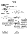
FIG. 13 is a flow chart for explaining a
rotational speed control based on a state within the
DRAM in this first embodiment. The process shown in
FIG. 13 is carried out by the MPU 12, and is related
to the step S11 shown in FIG. 5 which decides
whether or not the continuity of the access needs to
be judged.
In FIG. 13, a step S51 decides whether or
not a command issued from the host unit is a read
command #A1 with respect to the zone 1. If the
decision result in the step S51 is YES, a step S52
decides whether or not read data exist in the DRAM.
Initially, the data with respect to the read command
#A1 does not exist in the DRAM, and the data of the
read command #A1 is read from the optical disk 72,
and then, the optical disk unit carries out a
preread to read data following the read command #A1
into the DRAM. In other words, if the decision
result in the step S52 is NO, a step S56 decides
whether or not a preread is being carried out, and a
step S57 stops the preread if the decision result in
the step S56 is YES. If the decision result in the
step S56 is NO or after the step S57, a step S58
judges that the rotational speed is not changed
(switched), and the process advances to a read
process.
Next, when a read command #A2 is issued
from the host unit, the step S52 decides whether or
not the read data of the read command #A2 exist in
the DRAM. This time, the read data of the read
command #A2 is already read into the DRAM by the
preread, and thus, the read data of the read command
#A2 can be transferred from the DRAM without having
to read the read data from the optical disk 72.
Hence, if the decision result in the step S52 is YES,
a step S53 transfers the read data of the read
command #A2 from the DRAM to the host unit, and a
step S54 reports a normal end of the transfer to the
host unit. In this case, the operation on the
optical disk 72 and the operation with respect to
the host unit do not need to match, and for this
reason, the operation on the optical disk 72 becomes
inconspicuous from the point of view of the
operation of the host unit. Accordingly, a step S55
increases the rotational speed at this timing, and
the process then advances to the read process.
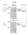
FIG. 14 is a diagram for explaining a
rotational speed increasing process and a read data
flow in this first embodiment. In FIG. 14, RD
denotes a read, CMD denotes a command, and a shaded
portion denotes a preread data. In addition, the
initial state of the DRAM is indicated by 1 ○, and a
next state of the DRAM is indicated by 2 ○.
Accordingly, during the read process, the
rotational speed for each zone is not switched
immediately. Instead, read hit target data in the
DRAM are monitored, and the rotational speed is
increased only when the hit target exists, while the
rotational speed is not increased if no hit target
exists. As a result, even when the read command is
received during the change of the rotational speed,
the read data in the DRAM are transferred so that
the change in the rotational speed does not affect
the host unit.
For example, the read commands from the
host unit include the following.
Next, when a write command #B1 with
respect to the zone 1 is received from the host unit,
the decision result in the step S51 becomes NO. In
this case, a step S59 transfers write data from the
host unit to the DRAM, and a step S60 decides
whether or not data to be transferred remains. If
the decision result in the step S60 is NO, a step
S63 judges that there is no change (switching) of
the rotational speed, and the process advances to a
write process. On the other hand, if the decision
result in the step S60 is YES, a step S61 reports a
normal end of the transfer to the host unit. In
addition, a step S62 increases the rotational speed,
and the process advances to the write process.
In other words, although a confirmation is
made to determine whether or not the write data
exist in the DRAM, no write is being made initially,
and thus, no write data exist in the DRAM. Hence,
the-write data of the write command #B1 are
transferred to the DRAM and are also written on the
optical disk 72. Then, the normal end of the
transfer is reported to the host unit at the same
time as when the transfer ends. In this state, the
operation on the optical disk 72 and the operation
with respect to the host unit do not need to match,
and for this reason, the operation on the optical
disk 72 becomes inconspicuous from the point of view
of the operation of the host unit. Accordingly, the
rotational speed is changed at this timing.
FIG. 15 is a diagram for explaining the
rotational speed increasing process and a write data
flow in this first embodiment. In FIG. 15, WRT
denotes a write, CMD denotes a command, and a shaded
portion denotes a vacant region. In addition, the
initial state of the DRAM is indicated by 1 ○, and a
next state of the DRAM is indicated by 2 ○.
Accordingly, during the write process, the
rotational speed for each zone is not switched
immediately. Instead, a vacant capacity in the DRAM
is monitored, and the rotational speed is increased
only when the vacant capacity exists, while the
rotational speed is not increased if no vacant
capacity exists. As a result, even when the write
command is received during the change of the
rotational speed, the write data are transferred to
the vacant regions of the DRAM so that the change in
the rotational speed does not affect the host unit.
For example, the write commands from the
host unit include the following.
... #Bn. Write Command: LBA=(1100h + 10h x n)/No.
of Blocks=10h
Next, a description will be given of
second through seventh embodiments of the storage
apparatus according to the present invention. The
construction of each of the second through seventh
embodiments of the storage apparatus is the same as
the construction of the first embodiment of the
storage apparatus described above in conjunction
with FIGS. 1 and 2, and an illustration thereof will
be omitted. In the second through seventh
embodiments of the storage apparatus, the present
invention is applied to an optical disk unit. In
addition, the second through seventh embodiments of
the storage apparatus respectively employ second
through seventh embodiments of the rotation control
method according to the present invention.
FIG. 16 is a flow chart for explaining the
rotational speed control based on a state within the
DRAM in the second embodiment. The process shown in
FIG. 16 is carried out by the MPU 12, and is related
to the step S11 shown in FIG. 5 which decides
whether or not the continuity of the access needs to
be judged. In FIG. 16, those steps which are the
same as those corresponding steps in FIG. 13 are
designated by the same reference numerals, and a
description thereof will be omitted. In addition,
an illustration of those steps carried out when the
command is the write command will be omitted in FIG.
16.
In this embodiment, a DRAM region is
regarded as one section, where one section is made
up of 200h blocks, as will be described later in
conjunction with FIG. 20. Furthermore, it is
assumed that the data transfer rate required by the
host unit is 0.4 Mbyte/s. In the following
description, BC denotes a block.
In FIG. 16, after the step S54, a step S60
decides whether or not the read hit target data in
the DRAM amounts to 80% or more of the DRAM region.
The process advances to the step S58 if the decision
result in the step S60 is NO, and the process
advances to the step S55 if the decision result in
the step S60 is YES.
In other words, when a read command #C1
with respect to the zone 1 is issued from the host
unit, a confirmation is made to determine whether or
not the read data exists in the DRAM. Initially,
the data with respect to the read command #C1 do not
exist in the DRAM, and thus, the data of the read
command #C1 are read from the optical disk 72. Then,
in optical disk unit, a preread is carried out to
read the data following the read command #C1 into
the DRAM.
Next, it is assumed for the sake of
convenience that a read command #C2 is issued from
the host unit. In this case, a confirmation is made
to determine whether or not the read data exists in
the DRAM, similarly as described above. This time,
however, data amounting to 30h blocks are already
read into the DRAM by the preread, and the data of
the read command #C2 can be transferred from the
DRAM to the host unit without having to read the
data from the optical disk 72. In the first
embodiment described above, the rotational speed is
changed at this timing, but there is a possibility
that only the data of LBA = 1100h to LBA = 113Fh
exist in the DRAM and a read command with respect to
the data which have not yet been read into the DRAM
may be received from the host unit during the
changing of the rotational speed. In such a
situation, it becomes necessary to read the data
from the optical disk 72 after the rotational speed
is changed, thereby delaying the transfer of the
data with respect to the host unit.
If a large amount of read data is held in
the DRAM region, it is possible to positively
transfer the data to the host unit from the DRAM.
Hence, in this second embodiment, the rotational
speed is changed when the read commands amounting to
W % or more of the DRAM region are held in the DRAM.
For example, when W = 80 %, the rotational speed is
changed if the read data amounting to 190h or more
are held in the DRAM, since the DRAM region amounts
to 200h.
FIG. 17 is a diagram showing read hit
target data and vacant regions of the DRAM. In FIG.
17, #1, ... denote read commands, and "vacant"
denotes the vacant region of the DRAM. In addition,
FIG. 18 is a diagram showing a table for managing
the read hit target data. In FIG. 18, #1, ...
denote read commands, a "BC Number" denotes the
number of blocks, and "ADR of First LBA" denotes an
address of the DRAM where the first LBA is stored.
The table shown in FIG. 18 may be stored in an
internal memory of the MPU 12 or, in a SRAM or the
like within the memory 18.
In the description of the third and
subsequent embodiments which will be given later,
the same designations are used as in FIGS. 17 and 18.
FIG. 19 is a flow chart for explaining a
process of investigating an amount of read hit
target data in the DRAM in the step S60 shown in FIG.
16. In FIG. 19, a step S61 sets the number of read
hit target blocks (BC number E0h of the read hit
target) to a sum of the BC number of the read
command #1, the BC number of the read command #2,
the BC number of the read command #3, and the BC
number of the read command #4, for example. A step
S62 decides whether or not the BC number (E0h) of
the read hit target is 80 % (190h) or more of the
total capacity of the DRAM, for example. If the
decision result in the step S62 is YES, it is judged
that the rotational speed can be changed, and the
process advances to the step S55 shown in FIG. 16.
On the other hand, if the decision result in the
step S62 is NO, it is judged that the rotational
speed cannot be changed, and the process advances to
the step S58 shown in FIG. 16.
When the read commands are processed
similarly up to a read command #C15, the read hit
target data in the DRAM amounts to 190h or more as
shown in FIG. 20, and the rotational speed is
changed at this timing. FIG. 20 is a diagram for
explaining a rotational speed increasing process and
the read hit target data in the DRAM in this second
embodiment. In FIG. 20, RD denotes a read, CMD
denotes a command, and a shaded portion denotes a
preread data.
Hence, during the read process, even if
the read hit target data exist in the DRAM, the
rotational speed is not switched immediately for
each zone, and the rotational speed is not increased
unless the read hit target data within the DRAM
amounts to W % or more of the total capacity of the
DRAM. Accordingly, even when the read command is
received during the change of the rotational speed,
the read data in the DRAM are transferred to the
host unit, so that the change of the rotational
speed will not affect the host unit.
For example, the read commands from the
host unit include the following.
... #Cn-1.Read Command: LBA=1130h/No. of Blocks=10h #Cn. Read Command: LBA=1190h/No. of Blocks=10h
...
FIG. 21 is a flow chart for explaining a
rotation control based on a state within the DRAM in
a third embodiment. The process shown in FIG. 21 is
carried out by the MPU 12, and is related to the
step S11 shown in FIG. 5 which decides whether or
not the continuity of the access needs to be judged.
In FIG. 21, those steps which are the same as those
corresponding steps in FIG. 13 are designated by the
same reference numerals, and a description thereof
will be omitted. Furthermore, an illustration of
those steps carried out when the command is the
write command will be omitted in FIG. 21.
In this embodiment, a DRAM region is
regarded as one section, where one section is made
up of 200h blocks, as will be described later in
conjunction with FIG. 26. Furthermore, it is
assumed that the data transfer rate required by the
host unit is 0.4 Mbyte/s. It is also assumed that a
time required for the change of the rotational speed
of the optical disk 72, that is, a time required for
the rotational speed to stabilize after the
rotational speed is switched, is 0.5 seconds (s),
for example. Moreover, the read hit target data in
the DRAM are limited to the sequential data, and the
rotational speed is changed when the amount of data
stored in the DRAM becomes greater than or equal to
a predetermined value, similarly as in the case of
the second embodiment described above.
In FIG. 21, when the command issued from
the host unit is a read command, a step S69 carries
out a read statistical information updating process
so as to update a total number T of sequential
blocks which will be described later, and the
process advances to the step S52. In addition,
after the step S54, a step S70 decides whether or
not the total number T of sequential blocks is
greater than or equal to a statistical information
reference value k. The process advances to the step
S58 if the decision result in the step S70 is NO,
and the process advances to a step S71 if the
decision result in the step S70 is YES. The step
S71 decides whether or not the read hit target data
in the DRAM amounts to 80 % or more of the total
capacity of the DRAM. The process advances to the
step S58 if the decision result in the step S71 is
NO, and the process advances to the step S55 if the
decision result in the step S71 is YES.
In other words, when a read command #D1
with respect to the zone 1 is first issued from the
host unit, access pattern information of the LBA and
the number of blocks is stored in the DRAM or the
SRAM within the memory 18, as the read statistical
information. Initially, the data with respect to
the read command #D1 do not exist in the DRAM, and
thus, the data of the read command #D1 are read from
the optical disk 72. Then, the optical disk unit
carries out a preread to read the data following the
read command #D1 into the DRAM. Next, when a read
command #D2 is issued from the host unit, the access
pattern information of the LBA and the number of
blocks is stored as the read statistical information,
and a confirmation is made to determine whether or
not the read data exist in the DRAM, similarly as
described above. This time, since the data
amounting to 40h blocks are already read into the
DRAM by the preread, the data of the read command
#D2 are transferred from the DRAM to the host unit,
without having to read the data from the optical
disk 72.
Next, when a read command #D3 is issued
from the host unit, a process is carried out
similarly as described above. Thereafter, when
similar processes are carried out with respect to
the read commands up to a read command #D10, the
read statistical information reaches the reference
value k. Various settings are possible for the
reference value k, but in this case, it is
determined that the access is a sequential read
access when the read commands are sequential and the
total number of processed blocks becomes 100h or
greater. In this state, the rotational speed is
changed when the read hit target data in the DRAM
amount to X % or more of the total capacity of the
DRAM, that is, the DRAM region. In this embodiment,
when X = 80 %, the rotational speed is changed when
the read hit target data in the DRAM amount to 190h
or more, but since the read hit target data only
amount to 120h in this state, the rotational speed
is not changed. When a read command #D23 is
received, sequential read hit target data amounting
to 190h or more exist in the DRAM as shown in FIG.
26, and the rotational speed is changed at this
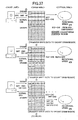
timing. FIG. 26 is a diagram for explaining the
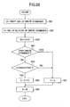
rotational speed increasing process and the read
data flow in this third embodiment. In FIG. 26, RD
denotes a read, CMD denotes a command, and a shaded
portion denotes a preread data. In addition, 1 ○
through 5 ○ respectively indicate the states of the
DRAM from the initial state to the state where the
read data are transferred.
FIG. 22 is a flow chart for explaining the
read statistical information updating process of the
step S69 shown in FIG. 21. In FIG. 22, R denotes a
last LBA of the read command, S denotes a last LBA
of the previous read command, and T denotes a total
number of sequential blocks.
In FIG. 22, a step S72 sets P to a first
LBA of the read command, and a step S73 sets Q to
the number of blocks of the read command. A step
S74 sets P + Q to R. A step S75 decides whether or
not the first read command is received. The process
advances to a step S76 if the decision result in the
step S75 is NO. The step S76 decides whether or not
P and S are consecutive. If the decision result in
the step S76 is YES, a step S77 increases the value
of T by setting T + Q to T. On the other hand, if
the decision result in the step S75 is YES or, if
the decision result in the step S76 is NO, a step
S78 clears the value of T by setting 0 to T. After
the step S77 or S78, a step S79 updates the value of
S by setting R to S, and the process ends.
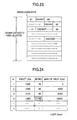
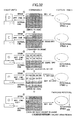
FIG. 23 is a diagram showing the read hit
target data and the vacant regions of the DRAM. In
addition, FIG. 24 is a diagram showing a table for
managing the read hit target data.
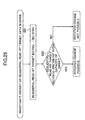
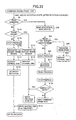
FIG. 25 is a flow chart for explaining the
process of investigating the amount of read hit
target data in the DRAM carried out by the step S71
shown in FIG. 21. In FIG. 25, a step S81 sets the
number of read hit target blocks (BC number 70h of
the read hit target) to the BC number of the read
command #4, for example. A step S82 decides whether
or not the BC number (70h) of the read hit target is
80 % (190h) or more of the total capacity of the
DRAM, for example. If the decision result in the
step S82 is YES, it is judged that the rotational
speed can be changed, and the process advances to
the step S55 shown in FIG. 16. On the other hand,
if the decision result in the step S82 is NO, it is
judged that the rotational speed cannot be changed,
and the process advances to the step S58 shown in
FIG. 16.
Accordingly, the command which is received
from the host unit while the rotational speed is
being changed is specified by detecting the
sequential read access, during the read process.
The change of the rotational speed will not affect
the host unit, by increasing the rotational speed
when the specified read data amount to X % or more
of the total capacity of the DRAM.
For example, the read commands from the
host unit include the following.
... #Dn. Read Command: LBA=(1100h + 20h x n)/No. of
Blocks=20h
FIG. 27 is a flow chart for explaining a
rotation control based on a state within the DRAM in
a fourth embodiment. The process shown in FIG. 27
is carried out by the MPU 12, and is related to the
step S11 shown in FIG. 5 which decides whether or
not the continuity of the access needs to be judged.
In FIG. 27, those steps which are the same as those
corresponding steps in FIG. 13 are designated by the
same reference numerals, and a description thereof
will be omitted. Furthermore, an illustration of
those steps carried out when the command is the read
command will be omitted in FIG. 21.
In this embodiment, a DRAM region is
regarded as one section, where one section is made
up of 200h blocks, as will be described later in
conjunction with FIG. 32. Furthermore, it is
assumed that the data transfer rate required by the
host unit is 0.4 Mbyte/s. It is also assumed that a
time required for the change of the rotational speed
of the optical disk 72, that is, a time required for
the rotational speed to stabilize after the
rotational speed is switched, is 0.5 seconds (s),
for example. Moreover, the read hit target data in
the DRAM are limited to the sequential data, and the
rotational speed is changed when the amount of
vacant regions in the DRAM becomes greater than or
equal to a predetermined value, similarly as in the
case of the first embodiment described above.
In FIG. 27, when the command issued from
the host unit is a write command, a step S85 carries
out a write statistical information updating process
to update a total number Y of sequential blocks
which will be described later, and the process
advances to the step S59. In addition, after the
step S61, a step S86 decides whether or not the
total number Y of sequential blocks is greater than
or equal to a statistical information reference
value 1. The process advances to the step S63 if
the decision result in the step S86 is NO, and the
process advances to a step S87 if the decision
result in the step S86 is YES. The step S87 decides
whether or not the vacant regions in the DRAM amount
to 80 % or more of the total capacity of the DRAM.
The process advances to the step S63 if the decision
result in the step S87 is NO, and the process
advances to the step S62 if the decision result in
the step S87 is YES.
In other words, when a write command #E1
with respect to the zone 1 is first issued from the
host unit, access pattern information of the LBA and
the number of blocks is stored in the DRAM or the
SRAM within the memory 18, as the write statistical
information. Initially, the write data with respect
to the write command #E1 do not exist in the DRAM,
and thus, the write data of the write command #E1
are transferred to the DRAM and a normal end of the
data transfer is reported to the host unit. In the
first embodiment which does not take into account
the sequential access, the rotational speed is
changed at this timing. However, in this fourth
embodiment, the rotational speed is changed only in
the case of the sequential write access, and thus,
the rotational speed is not changed in this state.
Then, when a write command #E2 is issued
from the host unit, the access pattern information
of the LBA and the number of blocks is stored as the
write statistical information, similarly as
described above. In addition, since the vacant
regions in the DRAM amount to 1F0h, the write data
of the write command #E2 are transferred to the DRAM,
and the normal end of the data transfer is reported
to the host unit. Thereafter, when similar
processes are carried out with respect to the write
commands up to a write command #E10, the write
statistical information reaches the reference value
1. Various settings are possible for the reference
value 1, but in this case, it is determined that the
access is a sequential write access when the write
commands are sequential and the total number of
processed blocks becomes 100h or greater. In this
state, the rotational speed is changed when the
vacant regions in the DRAM amount to X % or more of
the total capacity of the DRAM, that is, the DRAM
region. In this embodiment, when X = 80 %, the
rotational speed is changed when the vacant regions
in the DRAM amount to 190h or more, but since the
vacant regions only amount to E0h in this state, the
rotational speed is not changed. When a write
command #E23 is received, vacant regions amounting
to 190h or more exist in the DRAM as shown in FIG.
32, and the rotational speed is changed at this
timing. FIG. 32 is a diagram for explaining the
rotational speed increasing process and the write
data flow in this fourth embodiment. In FIG. 32,
WRT denotes a write, CMD denotes a command, and a
shaded portion denotes a vacant region of the DRAM.
In addition, 1 ○ through 5 ○ respectively indicate the
states of the DRAM from the initial state to the
state where the vacant regions amounting to 1E0h
exist in the DRAM.
FIG. 28 is a flow chart for explaining the
write statistical information updating process of
the step S85 shown in FIG. 27. In FIG. 28, W
denotes a last LBA of the write command, X denotes a
last LBA of the previous write command, and Y
denotes a total number of sequential blocks.
In FIG. 28, a step S91 sets U to a first
LBA of the write command, and a step S92 sets V to
the number of blocks of the write command. A step
S93 sets U + V to W. A step S94 decides whether or
not the first write command is received. The
process advances to a step S95 if the decision
result in the step S94 is NO. The step S95 decides
whether or not W and U are consecutive. If the
decision result in the step S95 is YES, a step S96
increases the value of Y by setting Y + V to Y. On
the other hand, if the decision result in the step
S94 is YES or, if the decision result in the step
S95 is NO, a step S97 clears the value of Y by
setting 0 to Y. After the step S96 or S97, a step
S98 updates the value of X by setting W to X, and
the process ends.
FIG. 29 is a diagram showing the write
data and the vacant regions of the DRAM. In
addition, FIG. 30 is a diagram showing a table for
managing the write data.
FIG. 31 is a flow chart for explaining the
process of investigating the amount of vacant
regions in the DRAM carried out by the step S87
shown in FIG. 27. In FIG. 31, a step S101 sets the
total number of blocks of the write data(BC number
E0h of the write data) to a sum of the BC number of
the write command #1, the BC number of the write
command #2, the BC number of the write command #3,
and the BC number of the write command #4, for
example. A step S102 sets the amount (120h) of
vacant regions in the DRAM to a value which is
obtained by subtracting the BC number (E0h) of the
write data from the total capacity (200h) of the
DRAM, for example. A step S103 decides whether or
not the vacant regions in the DRAM amounts to 80 %
(190h) or more of the total capacity of the DRAM,
for example. If the decision result in the step
S103 is YES, it is judged that the rotational speed
can be changed, and the process advances to the step
S62 shown in FIG. 27. On the other hand, if the
decision result in the step S103 is NO, it is judged
that the rotational speed cannot be changed, and the
process advances to the step S63 shown in FIG. 27.
Accordingly, it is possible to obtain the
effects of the change of the rotational speed by
detecting the sequential write access, during the
write process. The change of the rotational speed
will not affect the host unit, by changing the
rotational speed when the vacant regions in the DRAM
amount to X % or more of the total capacity of the
DRAM.
For example, the write commands from the
host unit include the following.
... #En. Write Command: LBA=(1100h + 20h x n)/No.
of Blocks=20h
When the rotational speed of the optical
disk 72 is changed, it takes a predetermined time
until the rotational speed stabilizes. Hence, in an
embodiment which will be described hereinafter, the
switching of the rotational speed is suppressed to a
minimum, so as to further improve the data transfer
efficiency.
FIG. 33 is a flow chart for explaining the
rotational speed control based on a state within the
DRAM in a fifth embodiment. The process shown in
FIG. 33 is carried out by the MPU 12, and is related
to the step S11 shown in FIG. 5 which decides
whether or not the continuity of the access needs to
be judged. In FIG. 33, those steps which are the
same as those corresponding steps in FIGS. 13 and 21
are designated by the same reference numerals, and a
description thereof will be omitted.
In this embodiment, the DRAM region
amounting to 400h is sectioned into two sections,
where each section is made up of 200h blocks, as
shown in FIGS. 34 and 35. Further, in this
embodiment, the high-speed rotation state is
continued after the rotational speed is increased by
one of the first through third embodiments described
above. In the first through third embodiments, only
one DRAM is used, but in this embodiment, one DRAM
is used by dividing the DRAM region into two regions
DRAM#1 and DRAM#2 or, two DRAMs, one having the
region DRAM#1 and the other having the region DRAM#2,
are used.
FIGS. 34 and 35 are diagrams for
explaining the continuation of the high-speed
rotation after the rotational speed increasing
process in the fifth embodiment. In FIGS. 34 and 35,
RD denotes a read, WRT denotes a write, CMD denotes
a command, a shaded portion denotes an preread data
in the DRAM, and a hatching portion denotes an
vacant region in the DRAM. Furthermore, 1 ○ through
5 ○ respectively indicate the states of the DRAM from
the initial state where the write data are
transferred to the vacant regions of the DRAM to the
state where the preread data amounting to 190h or
more are read into the DRAM.
In FIG. 33, after the step S57, a step
S111 decreases the rotational speed, and the process
advances to the read process. On the other hand, if
the decision result in the step S51 is NO, a step
S112 decides whether or not a vacant region exists
in the DRAM. If the decision result in the step
S112 is YES, a step S113 transfers the write data
from the host unit to the vacant region of the DRAM.
In addition, a step S114 reports a normal end of the
data transfer to the host unit, and the write
process assumes a standby state.
If the decision result in the step S112 is
NO, a step S115 stops the preread, and a step S116
transfers the write data from the host unit to the
vacant region of the DRAM. In addition, a step S117
reports a normal end of the data transfer to the
host unit. A step S118 decreases the rotational
speed, and the process advances to the write process.
When the preread is stopped, a step S120
decides whether or not unwritten data exist. If the
decision result in the step S120 is NO, the write
process assumes a command wait state which waits for
a command from the host unit. On the other hand, if
the decision result in the step S120 is YES, the
write process assumes a standby state.
When the write process assumes the standby
state and a waiting time of two seconds, for example,
elapses in a step S119, the process advances to the
write process.
In other words, after the rotational speed
is increased according to the third embodiment, for
example, the vacant regions of the DRAM are
confirmed when a write command #F1 with respect to
the zone 0 is issued form the host unit. Since the
preread is being made with respect to the zone 1 at
the high-speed rotation using the region DRAM#1, the
write data are transferred to the region DRAM#2.
After the data transfer, the normal end of the data
transfer is reported to the host unit, but the write
process is not carried out immediately, and the
preread of the region DRAM#1 is continued.
Next, when a read command #F2 is issued
from the host unit, the read statistical information
is updated, and a confirmation is thereafter made to
determine whether or not the read data exist in the
DRAM. In this case, the read data amounting to 40h
blocks are already read into the region DRAM#1 by
the preread, and thus, the read data are transferred
from the region DRAM#1 to the host unit.
Thereafter, when similar processes are
carried out with respect to the received commands up
to a write command #F61, no more vacant regions
exist in the DRAM. Hence, the preread is stopped,
the rotational speed is switched to that for the
zone 0, and the write data of the region DRAM#2 are
written on the optical disk 72.
When the writing of the write data in the
region DRAM#2 onto the optical disk 72 ends, a
vacant region is formed in the region DRAM#2, and
the write data of the write command #F61 are
transferred to the region DRAM#2. After the write
data of the write command #F61 are transferred, the
normal end of the data transfer is reported to the
host unit, but the write process is not carried out
immediately, and a command from the host unit is
waited for m seconds. In this embodiment, m = 2.
Accordingly, if a read command #F62 is issued from
the host unit within two seconds, the read
statistical information is updated since the read
data exist in the region DRAM#1, and then the read
data are transferred from the region DRAM#1 to the
host unit.
Thereafter, similar processes are carried
out with respect to the received commands up to a
read command #F65, and since no read data of a read
command #F66 exist in the DRAM, the data are read
from the optical disk 72 with respect to the read
command #F66. Then, the preread of the data
following the read command #F66 is carried out.
When similar processes are carried out with respect
to the commands following the read command #F66, the
read hit target data in the region DRAM#1 amounts to
120h or more, and since a sequential access is being
made, the rotational speed is changed again
similarly as in the case of the third embodiment
described above.
When processes similar to the above are
carried out thereafter and no command is received
from the host unit within two seconds, the write
data in the DRAM are written on the optical disk 72.
When the rotational speed is increased in response
to the read command and a command with respect to a
zone, other than the present zone, and in which the
rotational speed is to be decreased in particular is
received subsequently, the actual operation with
respect to the subsequent command is processed later
as much as possible, so as to continue the rotation
at the increased rotational speed. As a result, it
is possible to prevent the random access performance
and the data transfer rate from deteriorating due to
the change in the rotational speed, and the data
transfer efficiency can further be improved.
For example, the commands from the host
unit include the following.
... #Fn. Write Command: LBA=(100h + 20 x nh)/No. of
Blocks=20h
... #Fm. Read Command: LBA=(1120h + 20 x mh)/No. of
Blocks=20h #Fm+1. Read Command: LBA=(1120h + 40 x nh)/No.
of Blocks=20h
FIG. 36 is a flow chart for explaining the
rotational speed control based on a state within the
DRAM in a sixth embodiment. The process shown in
FIG. 36 is carried out by the MPU 12, and is related
to the step S11 shown in FIG. 5 which decides
whether or not the continuity of the access needs to
be judged. In FIG. 36, those steps which are the
same as those corresponding steps in FIGS. 27 and 33
are designated by the same reference numerals, and a
description thereof will be omitted.
In this embodiment, the DRAM region
amounting to 400h is sectioned into two sections,
where each section is made up of 200h blocks, as
shown in FIGS. 37 and 38. Further, in this
embodiment, the high-speed rotation state is
continued after the rotational speed is increased by
the first or fourth embodiment described above. In
the first and fourth embodiments, only one DRAM is
used, but in this embodiment, one DRAM is used by
dividing the DRAM region into two regions DRAM#1 and
DRAM#2 or, two DRAMs, one having the region DRAM#1
and the other having the region DRAM#2, are used.
FIGS. 37 and 38 are diagrams for
explaining the continuation of the high-speed
rotation after the rotational speed increasing
process in the sixth embodiment. In FIGS. 37 and 38,
WRT denotes a write, CMD denotes a command, and a
hatching portion denotes an vacant region in the
DRAM. Furthermore, 1 ○ through 5 ○ respectively
indicate the states of the DRAM from the initial
state where the write data are transferred to the
vacant regions of the DRAM to the state where the
data are written to the zone 0 of the optical disk
72.
In FIG. 36, when a write command is issued
from the host unit, the step S85 carries out the
write statistical information updating process, and
the process advances to the step S112. On the other
hand, when the write process ends, a step S120
decides whether or not unwritten data exist, and the
write process assumes a command wait state which
waits for a command from the host unit if the
decision result in the step S120 is NO. If the
decision result in the step S120 is YES, a step S122
decides whether or not the write data of the zone
identical to the zone of the previous write exist.
The write process ends if the decision result in the
step S122 is YES. If the decision result in the
step S122 is NO, the write process assumes the
command wait state which waits for the command from
the host unit. When the write process assumes the
wait state and a write waiting time of two seconds,
for example, elapses in a step S119, the write
process ends.
In other words, when a write command #G1
with respect to the zone 0 is issued from the host
unit after the rotational speed is increased
according to the fourth embodiment, for example, the
write statistical information is updated before
confirming the vacant regions of the DRAM. Since
the write with respect to the zone 1 (LBA = 13C0h to
161Fh) is carried out at the high-speed rotation
from the region DRAM#1, the write data are
transferred to the region DRAM#2. After this data
transfer ends, the normal end of the data transfer
is reported to the host unit. Then, when a write
command #G2 with respect to the zone 1 is issued
from the host unit, the write statistical
information is updated similarly as described above,
the write data are transferred to the vacant region
DRAM#2, and the normal end of the data transfer is
reported to the host unit. Thereafter, similar
processes are carried out with respect to the write
commands up to a write command #G7.
When the write from the region DRAM#1 ends,
the write with respect to the zone 1 in which the
write process can be continued at the high-speed
rotation is carried out with priority for the write
command #G2. Next, when a write command #G8 with
respect to the zone 0 is issued from the host unit,
the write statistical information is updated
similarly as described above, the write data are
transferred to the region DRAM#1 from which the
write is ended, and the normal end of the data
transfer is reported to the host unit. Thereafter,
similar processes are carried out with respect to
the write commands up to a write command #G13.
After the write with respect to the write
command #G2 ends, the write of the write data (of
the write commands #G4, #G6, #G8, #G10 and #G10)
with respect to the zone 1 is continuously carried
out with priority, and the high-speed rotation is
maintained. When all of the write with respect to
the zone 1 ends, the write with respect to the zone
0 is not carried out immediately, but a command from
the host unit is waited for a time of m seconds. In
this embodiment, m = 2, for example. Accordingly,
if a write command with respect to the zone 1 is
issued from the host unit within two seconds, the
write with respect to the zone 1 is continued and
carried out with priority. On the other hand, if a
write command with respect to a zone other than the
zone 1 is issued from the host unit, the write data
are transferred to the vacant regions of the DRAM,
the rotational speed is changed after waiting for
two seconds similarly as described above, and the
write with respect to the zone 0 is carried out
thereafter. In addition, when a write command with
respect to the zone 1 or other zones is issued from
the host unit and the rotational speed can be
changed, the rotational speed is increased depending
on the write statistical information and the vacancy
state of the DRAM region as in the fourth embodiment
described above.
Accordingly, when the rotational speed is
increased in response to the write command and a
command is received with respect to a zone which is
other than the present zone and in which the
rotational speed is to be decreased, the actual
operation with respect to this command is postponed,
so as to continue the rotation at the increased
rotational speed. As a result, it is possible to
prevent the random access performance and the data
transfer speed from deteriorating due to the change
in the rotational speed, to thereby further improve
the data transfer efficiency.
For example, the write commands from the
host unit include the following.
...
FIGS. 39 and 40 are flow charts for
explaining the rotational speed control based on a
state within the DRAM in a seventh embodiment. The
process shown in FIGS. 39 and 40 is carried out by
the MPU 12, and is related to the step S11 shown in
FIG. 5 which decides whether or not the continuity
of the access needs to be judged. In FIGS. 39 and
40, those steps which are the same as those
corresponding steps in FIGS. 27 and 36 are
designated by the same reference numerals, and a
description thereof will be omitted.
In this embodiment, the DRAM region
amounting to 400h is sectioned into two sections,
where each section is made up of 200h blocks, as
shown in FIGS. 37 and 38. Further, in this
embodiment, the high-speed rotation state is
continued after the rotational speed is increased by
the first or fourth embodiment described above. In
the first and fourth embodiments, only one DRAM is
used, but in this embodiment, one DRAM is used by
dividing the DRAM region into two regions DRAM#1 and
DRAM#2 or, two DRAMs, one having the region DRAM#1
and the other having the region DRAM#2, are used.
FIGS. 41 and 42 are diagrams for
explaining the continuation of the high-speed
rotation after the rotational speed increasing
process in the seventh embodiment. In FIGS. 41 and
42, WRT denotes a write, and CMD denotes a command.
Furthermore, 1 ○ through 4 ○ respectively indicate the
states of the DRAM from the initial state where the
write data of write commands #H1, ... are received
from the host unit while holding the write data of
write commands #I1 through #I3 in the DRAM, to the
state where the rotational speed is increased and
the write data of the write commands #H1, ... are
written to the optical disk 72. In addition, a
reference numeral 501 denotes the write data of the
write commands #H1, ... presently received from the
host unit and transferred to the DRAM, and a
reference numeral 502 denotes the write data of the
write commands #I1 through #I3 already transferred
to and held in the DRAM. It is assumed for the sake
of convenience that the write data of the write
commands #I1 and #I2 are written in the zone 0, the
write data of the write command #I3 are written in a
zone 2, and the write data of the write commands
#H1, ... are written in a zone 5.
The process shown in FIG. 39 is basically
the same as the process shown in FIG. 36, except
that the rotational speed of the optical disk 72 is
that of the normal mode, which has not been
increased, when the write command is issued from the
host unit and the step S85 carries out the write
statistical information updating process.
In addition, the process shown in FIG. 40
is essentially the same as the process shown in FIG.
27, except that the rotational speed of the optical
disk 72 is that of the normal mode, which has not
been increased, when the write process ends and the
step S86 is carried out. In the case of the process
shown in FIG. 40, however, if the decision result in
the step S87 is NO, a step S131 judges that the
rotational speed cannot be changed, before the
process advances to the step S63. Moreover, if the
decision result in the step S87 is YES, a step S132
judges that the rotational speed can be changed,
before the process advances to the step S122. In
addition, the process advances to the step S63 if
the decision result in the step S122 is NO, and the
process advances to the step S62 if the decision
result in the step S122 is YES.
In other words, the write commands from
the host unit include the following, for example.
... #Hn. Write Command: LBA=(1100h + 20h x n)/No.
of Blocks=20h: Zone 5
...
In this case, when the conditions for
changing the rotational speed are satisfied by the
write commands #H1, ..., the rotational speed is not
changed when the DRAM holds the write data for the
zones other than the zone in which the rotational
speed is to be changed, and the write data for the
zones other than the zone in which the rotational
speed is to be changed are written to the optical
disk 72 with priority at the existing rotational
speed. In other words, the write data of the write
commands #I1 and #I2 are written in the zone 0, and
the write data of the write command #I3 are written
in the zone 2. After all of the write data for the
zones other than the zone in which the rotational
speed is to be changed are written to the optical
disk 72, the write data for the zone in which the
rotational speed is to be changed are written to the
optical disk 72 after increasing the rotational
speed. As a result, the write data of the write
commands #H1, ... are written in the zone 5 after
increasing the rotational speed.
Therefore, when consecutive write commands
are received from the host unit in the fourth
embodiment described above, for example, the write
with respect to the other zones is carried out with
priority at the existing (present) rotational speed,
if the write data of the write commands with respect
to the other zones are held in the DRAM and the
conditions for changing the rotational speed are
satisfied by the consecutive write commands.
Consequently, it is possible to reduce the number of
times the rotational speed is changed, so as to
prevent the deterioration of the performance caused
by the change of the rotational speed.
In the embodiments described above, the
present invention is applied to an optical disk unit
which uses a magneto-optical disk. However, the
present invention is of course similarly applicable
to apparatuses which use disk-shaped recording media
such as phase-change type optical disks and magnetic
disks. In addition, the shape of the recording
medium is not limited to the disk-shape, and the
recording medium may have a card-shape or the like
with a spiral track or concentric tracks formed
similarly to the optical disk of the above described
embodiments.
Further, the present invention is not
limited to these embodiments, but various variations
and modifications may be made without departing from
the scope of the present invention.