EP1193678A2 - Driving method for electro-optical device, electro-optical device, and electronic apparatus - Google Patents

Driving method for electro-optical device, electro-optical device, and electronic apparatus Download PDF

Info

Publication number
EP1193678A2
EP1193678A2 EP01308340A EP01308340A EP1193678A2 EP 1193678 A2 EP1193678 A2 EP 1193678A2 EP 01308340 A EP01308340 A EP 01308340A EP 01308340 A EP01308340 A EP 01308340A EP 1193678 A2 EP1193678 A2 EP 1193678A2
Authority
EP
European Patent Office
Prior art keywords
electro
transistor
optical device
driving
signal
Prior art date
Legal status (The legal status is an assumption and is not a legal conclusion. Google has not performed a legal analysis and makes no representation as to the accuracy of the status listed.)
Withdrawn
Application number
EP01308340A
Other languages
German (de)
French (fr)
Other versions
EP1193678A3 (en
Inventor
Mutsumi Kimura
Current Assignee (The listed assignees may be inaccurate. Google has not performed a legal analysis and makes no representation or warranty as to the accuracy of the list.)
Seiko Epson Corp
Original Assignee
Seiko Epson Corp
Priority date (The priority date is an assumption and is not a legal conclusion. Google has not performed a legal analysis and makes no representation as to the accuracy of the date listed.)
Filing date
Publication date
Application filed by Seiko Epson Corp filed Critical Seiko Epson Corp
Publication of EP1193678A2 publication Critical patent/EP1193678A2/en
Publication of EP1193678A3 publication Critical patent/EP1193678A3/en
Withdrawn legal-status Critical Current

Links

Images

Classifications

    • GPHYSICS
    • G09EDUCATION; CRYPTOGRAPHY; DISPLAY; ADVERTISING; SEALS
    • G09GARRANGEMENTS OR CIRCUITS FOR CONTROL OF INDICATING DEVICES USING STATIC MEANS TO PRESENT VARIABLE INFORMATION
    • G09G3/00Control arrangements or circuits, of interest only in connection with visual indicators other than cathode-ray tubes
    • G09G3/20Control arrangements or circuits, of interest only in connection with visual indicators other than cathode-ray tubes for presentation of an assembly of a number of characters, e.g. a page, by composing the assembly by combination of individual elements arranged in a matrix no fixed position being assigned to or needed to be assigned to the individual characters or partial characters
    • G09G3/22Control arrangements or circuits, of interest only in connection with visual indicators other than cathode-ray tubes for presentation of an assembly of a number of characters, e.g. a page, by composing the assembly by combination of individual elements arranged in a matrix no fixed position being assigned to or needed to be assigned to the individual characters or partial characters using controlled light sources
    • G09G3/30Control arrangements or circuits, of interest only in connection with visual indicators other than cathode-ray tubes for presentation of an assembly of a number of characters, e.g. a page, by composing the assembly by combination of individual elements arranged in a matrix no fixed position being assigned to or needed to be assigned to the individual characters or partial characters using controlled light sources using electroluminescent panels
    • GPHYSICS
    • G09EDUCATION; CRYPTOGRAPHY; DISPLAY; ADVERTISING; SEALS
    • G09GARRANGEMENTS OR CIRCUITS FOR CONTROL OF INDICATING DEVICES USING STATIC MEANS TO PRESENT VARIABLE INFORMATION
    • G09G3/00Control arrangements or circuits, of interest only in connection with visual indicators other than cathode-ray tubes
    • G09G3/20Control arrangements or circuits, of interest only in connection with visual indicators other than cathode-ray tubes for presentation of an assembly of a number of characters, e.g. a page, by composing the assembly by combination of individual elements arranged in a matrix no fixed position being assigned to or needed to be assigned to the individual characters or partial characters
    • G09G3/22Control arrangements or circuits, of interest only in connection with visual indicators other than cathode-ray tubes for presentation of an assembly of a number of characters, e.g. a page, by composing the assembly by combination of individual elements arranged in a matrix no fixed position being assigned to or needed to be assigned to the individual characters or partial characters using controlled light sources
    • G09G3/30Control arrangements or circuits, of interest only in connection with visual indicators other than cathode-ray tubes for presentation of an assembly of a number of characters, e.g. a page, by composing the assembly by combination of individual elements arranged in a matrix no fixed position being assigned to or needed to be assigned to the individual characters or partial characters using controlled light sources using electroluminescent panels
    • G09G3/32Control arrangements or circuits, of interest only in connection with visual indicators other than cathode-ray tubes for presentation of an assembly of a number of characters, e.g. a page, by composing the assembly by combination of individual elements arranged in a matrix no fixed position being assigned to or needed to be assigned to the individual characters or partial characters using controlled light sources using electroluminescent panels semiconductive, e.g. using light-emitting diodes [LED]
    • G09G3/3208Control arrangements or circuits, of interest only in connection with visual indicators other than cathode-ray tubes for presentation of an assembly of a number of characters, e.g. a page, by composing the assembly by combination of individual elements arranged in a matrix no fixed position being assigned to or needed to be assigned to the individual characters or partial characters using controlled light sources using electroluminescent panels semiconductive, e.g. using light-emitting diodes [LED] organic, e.g. using organic light-emitting diodes [OLED]
    • G09G3/3225Control arrangements or circuits, of interest only in connection with visual indicators other than cathode-ray tubes for presentation of an assembly of a number of characters, e.g. a page, by composing the assembly by combination of individual elements arranged in a matrix no fixed position being assigned to or needed to be assigned to the individual characters or partial characters using controlled light sources using electroluminescent panels semiconductive, e.g. using light-emitting diodes [LED] organic, e.g. using organic light-emitting diodes [OLED] using an active matrix
    • G09G3/3258Control arrangements or circuits, of interest only in connection with visual indicators other than cathode-ray tubes for presentation of an assembly of a number of characters, e.g. a page, by composing the assembly by combination of individual elements arranged in a matrix no fixed position being assigned to or needed to be assigned to the individual characters or partial characters using controlled light sources using electroluminescent panels semiconductive, e.g. using light-emitting diodes [LED] organic, e.g. using organic light-emitting diodes [OLED] using an active matrix with pixel circuitry controlling the voltage across the light-emitting element
    • GPHYSICS
    • G09EDUCATION; CRYPTOGRAPHY; DISPLAY; ADVERTISING; SEALS
    • G09GARRANGEMENTS OR CIRCUITS FOR CONTROL OF INDICATING DEVICES USING STATIC MEANS TO PRESENT VARIABLE INFORMATION
    • G09G2300/00Aspects of the constitution of display devices
    • G09G2300/04Structural and physical details of display devices
    • G09G2300/0404Matrix technologies
    • G09G2300/0417Special arrangements specific to the use of low carrier mobility technology
    • GPHYSICS
    • G09EDUCATION; CRYPTOGRAPHY; DISPLAY; ADVERTISING; SEALS
    • G09GARRANGEMENTS OR CIRCUITS FOR CONTROL OF INDICATING DEVICES USING STATIC MEANS TO PRESENT VARIABLE INFORMATION
    • G09G2300/00Aspects of the constitution of display devices
    • G09G2300/08Active matrix structure, i.e. with use of active elements, inclusive of non-linear two terminal elements, in the pixels together with light emitting or modulating elements
    • G09G2300/0809Several active elements per pixel in active matrix panels
    • G09G2300/0842Several active elements per pixel in active matrix panels forming a memory circuit, e.g. a dynamic memory with one capacitor
    • GPHYSICS
    • G09EDUCATION; CRYPTOGRAPHY; DISPLAY; ADVERTISING; SEALS
    • G09GARRANGEMENTS OR CIRCUITS FOR CONTROL OF INDICATING DEVICES USING STATIC MEANS TO PRESENT VARIABLE INFORMATION
    • G09G2310/00Command of the display device
    • G09G2310/02Addressing, scanning or driving the display screen or processing steps related thereto
    • G09G2310/0243Details of the generation of driving signals
    • G09G2310/0251Precharge or discharge of pixel before applying new pixel voltage
    • GPHYSICS
    • G09EDUCATION; CRYPTOGRAPHY; DISPLAY; ADVERTISING; SEALS
    • G09GARRANGEMENTS OR CIRCUITS FOR CONTROL OF INDICATING DEVICES USING STATIC MEANS TO PRESENT VARIABLE INFORMATION
    • G09G3/00Control arrangements or circuits, of interest only in connection with visual indicators other than cathode-ray tubes
    • G09G3/20Control arrangements or circuits, of interest only in connection with visual indicators other than cathode-ray tubes for presentation of an assembly of a number of characters, e.g. a page, by composing the assembly by combination of individual elements arranged in a matrix no fixed position being assigned to or needed to be assigned to the individual characters or partial characters
    • GPHYSICS
    • G09EDUCATION; CRYPTOGRAPHY; DISPLAY; ADVERTISING; SEALS
    • G09GARRANGEMENTS OR CIRCUITS FOR CONTROL OF INDICATING DEVICES USING STATIC MEANS TO PRESENT VARIABLE INFORMATION
    • G09G3/00Control arrangements or circuits, of interest only in connection with visual indicators other than cathode-ray tubes
    • G09G3/20Control arrangements or circuits, of interest only in connection with visual indicators other than cathode-ray tubes for presentation of an assembly of a number of characters, e.g. a page, by composing the assembly by combination of individual elements arranged in a matrix no fixed position being assigned to or needed to be assigned to the individual characters or partial characters
    • G09G3/2007Display of intermediate tones
    • G09G3/2018Display of intermediate tones by time modulation using two or more time intervals
    • G09G3/2022Display of intermediate tones by time modulation using two or more time intervals using sub-frames

Definitions

  • the driving method includes: a setting step of supplying an on-signal for causing the switching transistor to be in an on-state to the switching transistor via the scanning line, and of supplying a set signal for selecting a conducting state or a non-conducting state of the driving transistor to the driving transistor via the data line and the switching transistor in accordance with a period for which the on-signal is supplied; and a resetting step of supplying an on-signal for causing the reset transistor to be in an on-state to the reset transistor via the scanning line so as to reset the driving transistor to the non-conducting state.
  • a gray-scale may be obtained by performing a plurality of set-reset operations, each set-reset operation including the setting step and the resetting step.
  • the setting step the state of the electro-optical element is selected, and in the resetting step, the period for which the selected state is retained is determined.
  • the set-reset operation is defined as the operation including the setting step and the resetting step.
  • the electro-optical element may be an organic electro-luminescence element.
  • a basic circuit used in an embodiment of the present invention includes a poly-crystal silicon thin-film transistor formed by a low-temperature process at 600°C or lower (low-temperature poly-Si TFT).
  • the low-temperature poly-Si TFT can be formed on a large, inexpensive glass substrate, and can integrate a driving circuit on a panel. Accordingly, it is suitable for manufacturing an electro-optical device, such as a luminescence display device. Additionally, the low-temperature poly-Si TFT is small, but has a high current supplying power. Accordingly, it is suitable for use in a high-precision current luminescence display device.
  • the present invention is also applicable to an electro-optical device driven by other types of transistors, such as an amorphous silicon thin-film transistor (a-Si TFT), a silicon-based transistor, and an organic thin-film transistor using an organic semiconductor.
  • An impurity such as phosphorus or boron, is implanted into the poly-crystalline silicon layer 2 by using the gate electrodes 4 according to a self-alignment process so as to form MOS transistors 5a and 5b.
  • the MOS transistors 5a and 5b are a p-type transistor and an n-type transistor, respectively.
  • the reset transistor is not shown in Fig. 5.
  • contact holes are formed, and a source electrode and a drain electrode 7 are formed (Fig. 5(c)).
  • a second interlayer insulating film 8 contact holes are formed, and a pixel electrode 9 comprising ITO is formed (Fig. 5(d)).
  • an organic electro-luminescence element is manufactured (Fig. 6(b)).
  • the roles of the adhesion layer 10 are to improve the adhesion between the substrate and the interlayer 11 and also to obtain an accurate luminescence area.
  • the roles of the interlayer 11 are to reduce the parasitic capacitance by separating the gate electrodes 4, the source electrodes, and the drain electrodes 7 from the anode 14, and also to perform precise patterning by controlling the surface wettability when forming the electron-hole implantation layer 12 and the luminescent layer 13 by a liquid-phase process.
  • Fig. 7 is a perspective view illustrating the configuration of a mobile personal computer to which the above-described electro-optical device is applied.
  • a personal computer 1100 includes a main unit 1104 provided with a keyboard 1102, and a display unit 1106.
  • the display unit 1106 is provided with the above-described electro-optical device 100.

Landscapes

  • Engineering & Computer Science (AREA)
  • Physics & Mathematics (AREA)
  • Computer Hardware Design (AREA)
  • General Physics & Mathematics (AREA)
  • Theoretical Computer Science (AREA)
  • Control Of Indicators Other Than Cathode Ray Tubes (AREA)
  • Electroluminescent Light Sources (AREA)
  • Control Of El Displays (AREA)

Abstract

The invention seeks to provide a method for implementing a gray-scale display of an electro-optical device according to a time ratio gray-scale method without providing reset lines. In an electro-optical device comprising, at an intersection of a scanning line and a data line, an electro-optical element, a driving transistor for driving the electro-optical element, a switching transistor for controlling the driving transistor, and a reset transistor having the function of resetting the driving transistor to a non-conducting state, a gray-scale is obtained by performing a plurality of set-reset operations, each set-reset operation comprising: a setting step of supplying an on-signal to the switching transistor via the scanning line, and of supplying a set signal for selecting a conducting state or a non-conducting state of the driving transistor to the driving transistor via the data line and the switching transistor in accordance with the on-signal; and a resetting step of supplying an on-signal for the reset transistor via the scanning line so as to reset the driving transistor to the non-conducting state.

Description

The present invention relates to a driving method for an organic electro-luminescence display device, a driving method for an electro-optical device suitable for use with a display device, such as an organic electro-luminescence display device, an electro-optical device, and an electronic apparatus provided with such an electro-optical device.
Attention is being given to organic electro-luminescence display devices using organic materials as luminescent materials of luminescent elements since they have a wide viewing angle, and will potentially meet market demands, i.e., demands for thinner, lighter, smaller, and lower power-consuming display devices.
Unlike conventional liquid crystal display devices, in organic electro-luminescence display devices, a luminescence state of the luminescent element must be controlled by a current. One such control method is the conductance control method (T. Shimoda, M. Kimura, et al., Proc. Asia Display 98, 217; M. Kimura, et al., IEEE Trans. Ele. Dev. 46, 2282 (1999); M. Kimura, et al., Proc. IDW 99, 171; and M. Kimura et al., Dig. AM-LCD 2000, to be published). In this method, the luminescence state of the luminescent element is controlled by a current value, which is an analog value, and more specifically, it is controlled by changing the potential applied to a gate electrode of a driving transistor for driving the luminescent element. When thin-film transistors having different current characteristics are used, however, the difference in the current characteristics of the individual transistors may sometimes directly result in non-uniformity in the luminescence state of the luminescent elements.
Accordingly, the area ratio gray-scale method (M. Kimura, et al., Proc. Euro Display '99 Late-News Papers, 71, Japanese Unexamined Patent Application Publication No.9-233107, M. Kimura, et al., Proc. IDW 99,171, M. Kimura, et al, J. SID, to be published; and M. Kimura, et al., Dig. AM-LCD 2000 to be published) has been proposed. In the area ratio gray-scale method, unlike the above-mentioned conductance control method, the luminescence state of the luminescent elements is controlled without using a luminescence state at an intermediate luminance. More specifically, in this method, the gray-scale is displayed as follows. Pixels disposed in a matrix are divided into a plurality of sub-pixels, and it is determined whether the luminescent elements contained in the sub-pixels are either in a complete luminescence state or a complete non-luminescence state. Then, among the plurality of sub-pixels, the total area of the sub-pixels in the complete luminescence state is changed. In the area ratio gray-scale method, it is not necessary to set an intermediate current value corresponding to the luminescence state of the intermediate luminance. Accordingly, the influence of the current characteristics of the transistors for driving the luminescent elements can be reduced, thereby achieving a uniform image quality. In this method, however, the number of gray-scale levels is restricted by the number of sub-pixels. For a greater number of gray-scale levels, pixels must be divided into a greater number of sub-pixels, which makes the pixel structure complicated.
Accordingly, the time ratio gray-scale method (M. Kimura, et al., Proc. IDW 99, 171; M. Kimura, et al., Dig. AM-LCD 2000, to be published; M. Mizukami, et al., Dig. SID 2000, 912; and K. Inukai, et al., Dig. SID 2000,924) has been proposed. In the time ratio gray-scale method, the representation of the gray-scale is implemented by changing the period for which the luminescent elements in one frame are in the complete luminescence state. Accordingly, unlike the area ratio gray-scale method, it is not necessary to provide many sub-pixels for obtaining a greater number of gray-scale levels, and also, the time ratio gray-scale method can be used together with the area ratio gray-scale method. Thus, it is expected that the time ratio gray-scale method will be a promising method for digitally displaying a gray-scale.
However, in the SES (Simultaneous-Erasing-Scan) time ratio gray-scale method, which is reported in "K. Inukai, et al., Dig. SID 2000,924", in addition to the scanning lines, reset lines are required, and thus, the luminescence area is disadvantageously reduced.
Accordingly, a first object of the present invention is to provide a method for implementing the representation of a gray-scale of an electro-optical device without reset lines, and in particular, to provide a method for implementing the representation of the gray-scale of an electro-optical device, such as an organic electro-luminescence display device, according to the time ratio gray-scale method. A second object of the present invention is to provide an electro-optical device driven by the above-described driving method.
In order to achieve the first object, a first driving method for an electro-optical device according to the present invention is a driving method for an electro-optical device which includes, at an intersection of a scanning line and a data line, an electro-optical element, a driving transistor for driving the electro-optical element, a switching transistor for controlling the driving transistor, and a reset transistor for resetting the driving transistor to a non-conducting state. The driving method includes: a setting step of supplying an on-signal for causing the switching transistor to be in an on-state to the switching transistor via the scanning line, and of supplying a set signal for selecting a conducting state or a non-conducting state of the driving transistor to the driving transistor via the data line and the switching transistor in accordance with a period for which the on-signal is supplied; and a resetting step of supplying an on-signal for causing the reset transistor to be in an on-state to the reset transistor via the scanning line so as to reset the driving transistor to the non-conducting state. Accordingly, by supplying the on-signal for the switching transistor and the on-signal for the reset transistor via the same scanning line, the luminescence period can suitably be set without a reset line. In this specification, the electro-optical element and the electro-optical device respectively indicate an element and a device in which the luminescence state or the optical characteristic is electrically controlled. Specific examples of the electro-optical device include display devices, such as luminescence display devices, liquid crystal display devices, and electrophoretic display devices.
Throughout the specification, the "step of supplying an on-signal to the switching transistor via the scanning line, and of supplying a set signal for selecting a conducting state or a non-conducting state of the driving transistor to the driving transistor via the data line and the switching transistor in accordance with the on-signal" is defined as the "setting step". The "step of resetting the driving transistor to the non-conducting state by supplying an on-signal for causing the reset transistor to be in the on-state to the reset transistor via the scanning line" is defined as the "resetting step".
According to a second driving method for an electro-optical device of the present invention, in the above-described driving method for an electro-optical device, the electro-optical device may further include a power line for supplying a current to the electro-optical element via the driving transistor, and one end of the reset transistor may be connected to the power line.
According to a third driving method for an electro-optical device of the present invention, the conductivity type of the switching transistor and the conductivity type of the reset transistor may be different from each other. More specifically, for example, if the switching transistor is n-type, the reset transistor is p-type. If the switching transistor is p-type, the reset transistor is n-type. Accordingly, by suitably selecting a high-potential signal or a low-potential signal, the switching transistor and the reset transistor can be complementarily operated.
According to a fourth driving method for an electro-optical device of the present invention, in the above-described driving method for an electro-optical device, the conductivity types of the switching transistor, the driving transistor, and the reset transistor may be respectively n-type, p-type, and p-type. That is, when a high-potential scanning signal is supplied, the switching transistor enters the on-state. When a low-potential scanning signal is supplied, the reset transistor enters the on-state. Thus, the switching transistor and the reset transistor can be complementarily operated.
According to a fifth driving method for an electro-optical device of the present invention, in the above-described driving method for an electro-optical device, a voltage VS corresponding to the on-signal for causing the switching transistor to be in the on-state, a voltage VR corresponding to the on-signal for causing the reset transistor to be in the on-state, and a voltage V0 corresponding to an off-signal for causing both the switching transistor and the reset transistor to be in an off-state may satisfy a relational expression: VS > V0 > VR.
According to a sixth driving method for an electro-optical device of the present invention, in the above-described driving method for an electro-optical device, the voltage VS, the voltage VR, and the voltage V0 may satisfy relational expressions: -VS ≈ VR, and V0 = 0 V (voltages). According to the driving methods for electro-optical devices set forth in claims 5 and 6, only by setting three voltage values, such as VS, V0, and VR, the on-off operation of the switching transistor and the on-off operation of the reset transistor can be performed.
According to a seventh driving method for an electro-optical device of the present invention, in the above-described driving method for an electro-optical device, while the switching transistor is in the on-state, the reset transistor is in the off-state, and, while the reset transistor is in the on-state, the switching transistor is in the off-state. With this arrangement, the state of the electro-optical element and the period for which the selected state is retained can precisely be set.
According to an eighth driving method for an electro-optical device of the present invention, in the above-described driving method for an electro-optical device, a gray-scale may be obtained by setting a time interval between the setting step and the resetting step. That is, the time interval between the setting step and the resetting step corresponds to the period for which the selected state of the electro-optical element is retained. Thus, by suitably setting this time interval, a gray-scale can be obtained.
According to a ninth driving method for an electro-optical device of the present invention, in the above-described driving method for an electro-optical device, a gray-scale may be obtained by performing a plurality of set-reset operations, each set-reset operation including the setting step and the resetting step. In the setting step, the state of the electro-optical element is selected, and in the resetting step, the period for which the selected state is retained is determined. Thus, by repeating a plurality of above-described set-reset operations, a multi-level gray-scale can be obtained. Throughout this specification, the set-reset operation is defined as the operation including the setting step and the resetting step.
According to a tenth driving method for an electro-optical device of the present invention, in the above-described driving method for an electro-optical device, the time interval between the setting step and the resetting step may be different for each of the plurality of set-reset operations.
According to an eleventh driving method for an electro-optical device of the present invention, in the above-described driving method for an electro-optical device, the time interval between the setting step and the resetting step for each of the plurality of set-reset operations may be completely different from the others, and the ratio of time intervals for the plurality of set-reset operations may be about 1:2: .. :2n (n is an integer of one or more) based on the minimum time interval. For example, if two set-reset operations with a time interval ratio of 1:2 are performed, four gray-scale levels, i.e., 0, 1, 2, 3, can be displayed. If two set-reset operations with a time interval ratio of 1:1 are performed, three gray-scale levels, i.e., 0, 1, and 2 can be displayed. That is, in this driving method for an electro-optical device, a maximum number of gray-scale levels can be obtained by a minimum number of set-reset operations. The time interval ratio does not have to precisely be 1:2: .. :2n (n is an integer of one or more), and may be sufficient to such a degree to satisfy a required gray-scale precision.
According to a twelfth driving method for an electro-optical device of the present invention, in the above-described driving method for an electro-optical device, the set signal may be a signal for setting the driving transistor to be in the conducting state rather than the signal for selecting the conducting state or the non-conducting state of the driving transistor. This means that an intermediate conducting state other than the two states, i.e., the conducting state and the non-conducting state, of the driving transistor is selectable. This can be implemented by supplying the set signal as a signal having three or more consecutive or discrete values. This driving method is effective for implementing many gray-scale levels.
According to a thirteenth driving method for an electro-optical device of the present invention, in the above-described driving method for an electro-optical device, the electro-optical element may be an organic electro-luminescence element. The organic electro-luminescence element is a luminescent element using an organic material as an electric-field luminescent material.
A first electro-optical device of the present invention is driven by the above-described driving method for an electro-optical device. That is, in this electro-optical device, by supplying the on-signal for the switching transistor and the on-signal for the reset transistor via the same scanning line, the period for which the state of the electro-optical element selected in the setting step can suitably be set without a reset line.
A second electro-optical device of the present invention is an electro-optical device including, at an intersection of a scanning line and a data line, an electro-optical element, a driving transistor for driving the electro-optical element, a switching transistor for controlling the driving transistor, and a reset transistor for resetting the driving transistor to a non-conducting state. The electro-optical device includes at least one drive circuit for generating a signal for setting the switching transistor and the reset transistor to be in an on-state or an off-state, and for generating a signal for setting the driving transistor in accordance with the signal for setting the switching transistor to be in the on-state. It is not essential that only the single drive circuit is used for "generating a signal for setting the switching transistor and the reset transistor to be in an on-state or an off-state, and for generating a signal for setting the driving transistor in accordance with the signal for setting the switching transistor to be in the on-state". A plurality of drive circuits may be used.
A third electro-optical device of the present invention is an electro-optical device including, at an intersection of a scanning line and a data line, an electro-optical element, a driving transistor for driving the electro-optical element, a switching transistor for controlling the driving transistor, and a reset transistor for resetting the driving transistor to a non-conducting state. The electro-optical device includes: a scanning line driver for supplying a signal for setting the switching transistor and the reset transistor to be in an on-state or an off-state to the scanning line; and a data line driver for supplying a signal for setting the driving transistor to the data line in accordance with an operation of the scanning line driver.
A fourth electro-optical device of the present invention is an electro-optical device including, at an intersection of a scanning line and a data line, an electro-optical element, a driving transistor for driving the electro-optical element, a switching transistor for controlling the driving transistor, and a reset transistor for resetting the driving transistor to a non-conducting state. An on-signal for performing a setting step of setting a display condition of the electro-optical element is supplied to the switching transistor via the scanning line, and an on-signal for performing a resetting step of resetting a display condition of the electro-optical element is supplied to the reset transistor via the scanning line. In the above description, the definitions of the "setting step" and the "resetting step" are substantially similar to those of the setting step and the resetting step set forth in claim 1.
In the above-described electro-optical device, a fifth electro-optical device of the present invention may further include a power line for supplying a current to the electro-optical element via the driving transistor, and one end of the reset transistor may be connected to the power line. Accordingly, the first through fifth electro-optical devices of the present invention do not require a reset line for performing the time ratio gray-scale method. Advantageously, therefore, it is possible to ensure a sufficient display area. If more gray-scale levels are required, the time ratio gray-scale method can be employed with the area ratio gray-scale method by providing sub pixels in the pixels of the electro-optical device.
According to a sixth electro-optical device of the present invention, in the above-described electro-optical device, the electro-optical element may be an organic electro-luminescence element.
A first electronic apparatus of the present invention is an electronic apparatus in which the above-described electro-optical device is installed.
Embodiments of the present invention will now be described by way of further example only and with reference to the accompanying drawings, in which:-
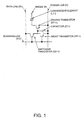
  • Fig. 1 illustrates a pixel equivalent circuit of an electro-optical device according to an embodiment of the present invention.
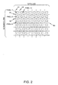
  • Fig. 2 illustrates a pixel arrangement of an electro-optical device according to an embodiment of the present invention.
  • Fig. 3 illustrates a driving method for an electro-optical apparatus according to an embodiment of the present invention.
  • Fig. 4 illustrates current characteristics of a luminescent element according to an embodiment of the present invention.
  • Fig. 5 illustrates part of a manufacturing process for an electro-optical device according to an embodiment of the present invention.
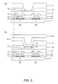
  • Fig. 6 illustrates part of a manufacturing process for an electro-optical device according to an embodiment of the present invention.
  • Fig. 7 illustrates an example of an electro-optical device of an embodiment of the present invention applied to a mobile personal computer.
  • Fig. 8 illustrates an example of an electro-optical device of an embodiment of the present invention applied to a display unit of a cellular telephone.
  • Fig. 9 is a perspective view illustrating a digital still camera having a finder to which an electro-optical device of an embodiment of the present invention is applied.
  • Preferable embodiments of the present invention are described below.
    A basic circuit used in an embodiment of the present invention includes a poly-crystal silicon thin-film transistor formed by a low-temperature process at 600°C or lower (low-temperature poly-Si TFT). The low-temperature poly-Si TFT can be formed on a large, inexpensive glass substrate, and can integrate a driving circuit on a panel. Accordingly, it is suitable for manufacturing an electro-optical device, such as a luminescence display device. Additionally, the low-temperature poly-Si TFT is small, but has a high current supplying power. Accordingly, it is suitable for use in a high-precision current luminescence display device. The present invention is also applicable to an electro-optical device driven by other types of transistors, such as an amorphous silicon thin-film transistor (a-Si TFT), a silicon-based transistor, and an organic thin-film transistor using an organic semiconductor.
    The equivalent circuit of one pixel of an electro-optical device according to an embodiment of the present invention is shown in Fig. 1. In this electro-optical device, a scanning line (S1), a data line (D1), and a power line (V) are formed, and a luminescent element (L11), a driving transistor (DT11) for driving the luminescent element (L11), a switching transistor (ST11) for controlling the driving transistor (DT11), a reset transistor (RT11) for resetting the driving transistor (DT11), and a capacitor (C11) are provided at the intersection of the scanning line (S1) and the data line (D1). One end of the luminescent element (L11) is connected to an anode (A). The driving transistor (DT11) is p-type. Accordingly, the driving transistor (DT11) enters a conducting state selected by a low-potential data signal to cause the luminescent element (L11) to be in the luminescence state. In contrast, the driving transistor (DT11) enters a non-conducting state by a selected high-potential data signal to cause the luminescent element (L11) to be in the non-luminescence state. In the pixel equivalent circuit shown in Fig. 1, the switching transistor (ST11), the driving transistor (DT11), and the reset transistor (RT11) are n-type, p-type, and p-type; respectively. However, this is not a limitation to implement the present invention.
    Fig. 2 illustrates the wiring and the pixel arrangement of an electro-optical device according to an embodiment of the present invention. Pixels are arranged in a matrix by a plurality of scanning lines (S1, S2, ....) and a plurality of data lines (D1, D2, ....), and a plurality of pixels are formed at corresponding intersections of the scanning lines and the data lines. For example, a pixel 11 is provided at the intersection of S1 and D1. Basically, the pixel includes a switching transistor (ST11), a reset transistor (RT11), a capacitor (C11), a driving transistor (DT11), and a luminescent element (L11), such as those shown in Fig. 1. However, the pixel may include a plurality of sub-pixels. A power line (V) is not shown in Fig. 2.
    Fig. 3 illustrates a driving method for an electro-optical device which includes the circuit shown in Fig. 1 and the pixel arrangement shown in Fig. 2 according to an embodiment of the present invention. A first scanning signal SS(S1) is supplied to the first scanning line (S1). A second scanning signal SS(S2) is supplied to the second scanning line (S2). A third scanning signal SS(S3) is supplied to the third scanning line (S3). A first data signal DS(D1) is supplied to the first data line (D1). A second data signal DS(D2) is supplied to the second data line (D2). A third data signal DS(D3) is supplied to the third data line (D3).
    In this embodiment, the switching transistor (ST11), the driving transistor (D11), and the reset transistor (RT11) are n-type, p-type, and p-type, respectively. Accordingly, a high-potential scanning signal serves as an on-signal for causing the switching signal to enter the conducting state. Then, a low-potential set signal indicated by the hatched portions in Fig. 3 is supplied in accordance with the on-signal for the switching transistor. According to this setting step, the driving transistor enters the conducting state so as to cause the luminescent element to emit light. In contrast, the low-potential scanning signal serves as an on-signal for the reset transistor. According to this resetting step, a high potential is applied to the p-type driving transistor from the power line via the reset transistor so as to cause the driving transistor to enter the non-conducting state. Thus, the luminescence element enters the non-luminescence state.
    The luminescence periods E1, E2, and E3 are defined by the time interval between the setting step and the resetting step. The ratio of the luminescence periods E1, E2, and E3 is set to be about 1:2:4. As a result, eight gray-scale levels, such as 0, 1, 2, 3, 4, 5, 6, and 7, are obtained. In this embodiment, the set-reset operations are sequentially performed such that the time interval between the setting step and the resetting step is increased. However, the set-reset operations do not have to be performed in this order, and it can be performed according to the circumstances of the use or the specifications. It may take some time for the transistor or the luminescent element to respond to the corresponding signal. Accordingly, as shown in Fig. 3, the start time and the end time of the luminescence period may be displaced from the start of the setting step and the start of the resetting step, respectively. In Fig. 3, the period for which the on-signal for the switching transistor is supplied coincides with the period for which the set signal is supplied. However, depending on the circumstances of the use or the specifications, the on-signal does not always have to coincide with the set signal.
    Fig. 4 illustrates the current characteristics of the luminescent element according to an embodiment of the present invention. The horizontal axis represents the control potential (Vsig) supplied to the gate electrode of the driving transistor, and the vertical axis designates the current value (IIep) of the organic electro-luminescence element. The current value and the luminance of the organic electro-luminescence element are substantially proportional to each other. Thus, it can be considered that the vertical axis also indicates the luminance. In this embodiment, it is preferable that the organic electro-luminescence element is unambiguously controlled to be in either the on state or the off state. When the electro-luminescence element is unambiguously in the on state or in the off state, the current value (IIep) is substantially constant even if the transistor characteristics are changed. Thus, the current value of the luminescent element does not change, and accordingly, the luminance substantially becomes uniform. Therefore, the image quality can be uniform.
    Fig. 5 illustrates a manufacturing process for a thin-film transistor for use in the electro-optical device according to an embodiment of the present invention. Amorphous silicon is first formed on a glass substrate 1 by PECVD using SiH4 or by LPCVD using Si2H6. The amorphous silicon is poly-crystallized by a laser, such as an excimer laser, or by solid-phase growth, thereby forming a poly-crystalline silicon layer 2 (Fig. 5(a)). After the poly-crystalline silicon layer 2 is patterned, a gate insulating film 3 is formed, and gate electrodes 4 are further formed (Fig. 5(b)). An impurity, such as phosphorus or boron, is implanted into the poly-crystalline silicon layer 2 by using the gate electrodes 4 according to a self-alignment process so as to form MOS transistors 5a and 5b. The MOS transistors 5a and 5b are a p-type transistor and an n-type transistor, respectively. The reset transistor is not shown in Fig. 5. After a first interlayer insulating film 6 is formed, contact holes are formed, and a source electrode and a drain electrode 7 are formed (Fig. 5(c)). Then, after a second interlayer insulating film 8 is formed, contact holes are formed, and a pixel electrode 9 comprising ITO is formed (Fig. 5(d)).
    Fig. 6 illustrates a manufacturing process for pixels used in the electro-optical device according to an embodiment of the present invention. First, an adhesion layer 10 is formed, and an opening corresponding to a luminescent region is formed. An interlayer 11 is then formed, and an opening is formed (Fig. 6(a)). Then, the wettability of the substrate surface is controlled by performing plasma processing using, for example, oxygen plasma or CF4 plasma. Subsequently, an electron-hole implantation layer 12 and a luminescent layer 13 are formed by a liquid-phase process, such as a spin coating, squeegee, or ink-jet process, or a vacuum process, such as sputtering or deposition. An anode 14 containing metal, such as aluminum, is then formed. Finally, a sealing layer 15 is formed. Thus, an organic electro-luminescence element is manufactured (Fig. 6(b)). The roles of the adhesion layer 10 are to improve the adhesion between the substrate and the interlayer 11 and also to obtain an accurate luminescence area. The roles of the interlayer 11 are to reduce the parasitic capacitance by separating the gate electrodes 4, the source electrodes, and the drain electrodes 7 from the anode 14, and also to perform precise patterning by controlling the surface wettability when forming the electron-hole implantation layer 12 and the luminescent layer 13 by a liquid-phase process.
    Some examples of electronic apparatuses using the above-described electro-optical device are described below. Fig. 7 is a perspective view illustrating the configuration of a mobile personal computer to which the above-described electro-optical device is applied. In Fig. 7, a personal computer 1100 includes a main unit 1104 provided with a keyboard 1102, and a display unit 1106. The display unit 1106 is provided with the above-described electro-optical device 100.
    Fig. 8 is a perspective view illustrating a configuration of a cellular telephone having a display unit to which the aforementioned electro-optical device 100 is applied. In Fig. 8, a cellular telephone 1200 includes, not only a plurality of operation buttons 1202, but also the above-described electro-optical device 100 together with an earpiece 1204 and a mouthpiece 1206.
    Fig. 9 is a perspective view illustrating a configuration of a digital still camera having a finder to which the above-described electro-optical device 100 is applied. Fig. 9 also schematically illustrates the connection of the digital still camera with external devices. In a regular camera, a film is exposed to light by an optical image of a subject. In a digital still camera 1300, however, an optical image of a subject is photoelectrically converted by an image pickup device, such as a CCD (Charge Coupled Device), so as to generate an imaging signal. On the rear surface of a casing 1302 of the digital still camera 1300, the aforementioned electro-optical device 100 is provided to display the subject based on the imaging signal obtained by the CCD. That is, the electro-optical device 100 serves as a finder for displaying the subject. On the observation side (on the reverse surface in Fig. 9) of the casing 1302, a photodetector unit 1304 including an optical lens and a CCD is disposed.
    A photographer checks the subject displayed on the electro-optical device 100 and presses a shutter button 1306. Then, an imaging signal obtained by the CCD is transferred to and stored in a memory of a circuit board 1308. In this digital still camera 1300, a video signal output terminal 1312 and a data communication input/output terminal 1314 are provided on the side surface of the casing 1302. Then, as shown in Fig. 9, a television monitor 1430 and a personal computer 1440 are connected to the video signal output terminal 1312 and the data communication input/output terminal 1314, respectively, as required. The imaging signal stored in the memory of the circuit board 1308 is output to the television monitor 1430 or the personal computer 1440 by a predetermined operation.
    Electronic apparatuses to which the electro-optical device 100 of the present invention is applicable include, not only the personal computer shown in Fig. 7, the cellular telephone shown in Fig. 8, and the digital still camera shown in Fig. 9, but also a liquid crystal television, a view-finder-type or direct-view-type video cassette recorder, a car navigation system, a pager, an electronic diary, a calculator, a word processor, a workstation, a videophone, a POS terminal, a device provided with a touch panel, for example. It is needless to say that the above-described electro-optical device 100 is applicable to the display units of these electronic apparatuses.

    Claims (20)

    1. A driving method for an electro-optical device which comprises, at an intersection of a scanning line and a data line, an electro-optical element, a driving transistor for driving the electro-optical element, a switching transistor for controlling the driving transistor, and a reset transistor for resetting the driving transistor to a non-conducting state, the driving method comprising:
      a setting step of supplying an on-signal for causing the switching transistor to be in an on-state to the switching transistor via the scanning line, and of supplying a set signal for selecting a conducting state or a non-conducting state of the driving transistor to the driving transistor via the data line and the switching transistor in accordance with a period for which the on-signal is supplied; and
      a resetting step of supplying an on-signal for causing the reset transistor to be an on-state to the reset transistor via the scanning line so as to reset the driving transistor to the non-conducting state.
    2. A driving method for an electro-optical device according to claim 1, wherein the electro-optical device further comprises a power line for supplying a current to the electro-optical element via the driving transistor, and one end of the reset transistor is connected to the power line.
    3. A driving method for an electro-optical device according to claim 1 or 2, wherein a conductivity type of the switching transistor and a conductivity type of the reset transistor are different from each other.
    4. A driving method for an electro-optical device according to any one of claims 1 to 3, wherein conductivity types of the switching transistor, the driving transistor, and the reset transistor are respectively n-type, p-type, and p-type.
    5. A driving method for an electro-optical device according to claim 4, wherein a voltage VS corresponding to the on-signal for causing the switching transistor to be in the on-state, a voltage VR corresponding to the on-signal for causing the reset transistor to be in the on-state, and a voltage V0 corresponding to an off-signal for causing the switching transistor and the reset transistor to be in an off-state satisfy a relational expression: VS > V0 > VR.
    6. A driving method for an electro-optical device according to claim 5, wherein the voltage VS, the voltage VR, and the voltage V0 satisfy relational expressions: -VS ≈ VR, and V0 = 0 V (voltages).
    7. A driving method for an electro-optical device according to any one of claims 1 to 6, wherein, while the switching transistor is in the on-state, the reset transistor is in the off-state, and, while the reset transistor is in the on-state, the switching transistor is in the off-state.
    8. A driving method for an electro-optical device according to any one of claims 1 to 7, wherein a gray-scale is obtained by setting a time interval between the setting step and the resetting step.
    9. A driving method for an electro-optical device according to any one of claims 1 to 8, wherein a gray-scale is obtained by performing a plurality of set-reset operations, each set-reset operation comprising the setting step and the resetting step.
    10. A driving method for an electro-optical device according to claim 9, wherein the time interval between the setting step and the resetting step is different for each of the plurality of set-reset operations.
    11. A driving method for an electro-optical device according to claim 9 or 10, wherein the time interval between the setting step and the resetting step for each of the plurality of set-reset operations is completely different fromthe others, and the ratio of time intervals for the plurality of set-reset operations is about 1:2: .. :2n (n is an integer of one or more) based on the minimum time interval.
    12. A driving method for an electro-optical device according to any one of claims 1 to 11, wherein the set signal is a signal for setting the driving transistor to the conducting state rather than the signal for selecting the conducting state or the non-conducting state of the driving transistor.
    13. A driving method for an electro-optical device according to any one of claims 1 to 12, wherein the electro-optical element comprises an organic electro-luminescence element.
    14. An electro-optical device driven by the driving method set forth in any one of claims 1 to 13.
    15. An electro-optical device including, at an intersection of a scanning line and a data line, an electro-optical element, a driving transistor for driving the electro-optical element, a switching transistor for controlling the driving transistor, and a reset transistor for resetting the driving transistor to a non-conducting state, the electro-optical device comprising at least one drive circuit for generating a signal for setting the switching transistor and the reset transistor to be in an on-state or an off-state, and for generating a signal for setting the driving transistor in accordance with the signal for setting the switching transistor to be in the on-state.
    16. An electro-optical device including, at an intersection of a scanning line and a data line, an electro-optical element, a driving transistor for driving the electro-optical element, a switching transistor for controlling the driving transistor, and a reset transistor for resetting the driving transistor to a non-conducting state, the electro-optical device comprising:
      a scanning line driver for supplying a signal for setting the switching transistor and the reset transistor to be in an on-state or an off-state to the scanning line; and
      a data line driver for supplying a signal for setting the driving transistor to the data line in accordance with an operation of the scanning line driver.
    17. An electro-optical device comprising, at an intersection of a scanning line and a data line, an electro-optical element, a driving transistor for driving the electro-optical element, a switching transistor for controlling the driving transistor, and a reset transistor for resetting the driving transistor to a non-conducting state,
         wherein an on-signal for performing a setting step of setting the electro-optical element is supplied to the switching transistor via the scanning line, and an on-signal for performing a resetting step of resetting the electro-optical element is supplied to the reset transistor via the scanning line.
    18. An electro-optical device according to any one of claims 15 to 17, wherein the electro-optical device further comprises a power line for supplying a current to the electro-optical element via the driving transistor, and one end of the reset transistor is connected to the power line.
    19. An electro-optical device according to any one of claims 15 to 18, wherein the electro-optical element comprises an organic electro-luminescence element.
    20. An electronic apparatus in which the electro-optical device set forth in any one of claims 14 to 19 is installed.
    EP01308340A 2000-09-29 2001-09-28 Driving method for electro-optical device, electro-optical device, and electronic apparatus Withdrawn EP1193678A3 (en)

    Applications Claiming Priority (4)

    Application Number Priority Date Filing Date Title
    JP2000300859 2000-09-29
    JP2000300859 2000-09-29
    JP2001294718A JP2002175048A (en) 2000-09-29 2001-09-26 Driving method of electro-optical device, electro-optical device, and electronic apparatus
    JP2001294718 2001-09-26

    Publications (2)

    Publication Number Publication Date
    EP1193678A2 true EP1193678A2 (en) 2002-04-03
    EP1193678A3 EP1193678A3 (en) 2002-08-28

    Family

    ID=26601259

    Family Applications (1)

    Application Number Title Priority Date Filing Date
    EP01308340A Withdrawn EP1193678A3 (en) 2000-09-29 2001-09-28 Driving method for electro-optical device, electro-optical device, and electronic apparatus

    Country Status (4)

    Country Link
    EP (1) EP1193678A3 (en)
    JP (1) JP2002175048A (en)
    KR (1) KR100457832B1 (en)
    TW (1) TWI271117B (en)

    Cited By (4)

    * Cited by examiner, † Cited by third party
    Publication number Priority date Publication date Assignee Title
    EP1372136A1 (en) * 2002-06-12 2003-12-17 Seiko Epson Corporation Scan driver and a column driver for active matrix display device and corresponding method
    WO2004109644A1 (en) * 2003-06-05 2004-12-16 Koninklijke Philips Electronics N.V. Display device addressing method
    US7928945B2 (en) 2003-05-16 2011-04-19 Semiconductor Energy Laboratory Co., Ltd. Display device and driving method thereof
    US9093571B2 (en) 2005-04-15 2015-07-28 Semiconductor Energy Laboratory Co., Ltd. Display device and electronic device using the same

    Families Citing this family (11)

    * Cited by examiner, † Cited by third party
    Publication number Priority date Publication date Assignee Title
    JP2004095671A (en) * 2002-07-10 2004-03-25 Seiko Epson Corp Thin film transistor, switching circuit, active element substrate, electro-optical device, electronic device, thermal head, droplet discharge head, printing device, thin film transistor driven light emitting display device
    JP2004139042A (en) * 2002-09-24 2004-05-13 Seiko Epson Corp Electronic circuit, electro-optical device, method of driving electro-optical device, and electronic apparatus
    JP4172250B2 (en) * 2002-11-01 2008-10-29 セイコーエプソン株式会社 Electro-optical device, driving method of electro-optical device, and electronic apparatus
    JP4618986B2 (en) * 2003-05-16 2011-01-26 株式会社半導体エネルギー研究所 Display device
    JP4646187B2 (en) * 2004-02-12 2011-03-09 東北パイオニア株式会社 Light emitting display device and drive control method thereof
    DE102005056255A1 (en) * 2005-11-25 2007-06-06 Patent-Treuhand-Gesellschaft für elektrische Glühlampen mbH Circuit device with overhead buck transistor
    EP1806724A3 (en) 2006-01-07 2009-10-07 Semiconductor Energy Laboratory Co., Ltd. Semiconductor device, display device and electronic device
    JP4994022B2 (en) * 2006-01-07 2012-08-08 株式会社半導体エネルギー研究所 Semiconductor device
    JP5151172B2 (en) * 2007-02-14 2013-02-27 ソニー株式会社 Pixel circuit and display device
    JP5244879B2 (en) * 2010-09-24 2013-07-24 株式会社半導体エネルギー研究所 Display device
    JP6041286B2 (en) * 2011-08-25 2016-12-07 株式会社Joled Display device and driving method thereof

    Family Cites Families (7)

    * Cited by examiner, † Cited by third party
    Publication number Priority date Publication date Assignee Title
    JP2571614B2 (en) * 1988-10-12 1997-01-16 シャープ株式会社 Display device drive circuit
    US5798746A (en) * 1993-12-27 1998-08-25 Semiconductor Energy Laboratory Co., Ltd. Liquid crystal display device
    JPH08201769A (en) * 1995-01-24 1996-08-09 Canon Inc Liquid crystal display
    JP3834086B2 (en) * 1995-11-06 2006-10-18 シャープ株式会社 Matrix type display device and driving method thereof
    US6489952B1 (en) * 1998-11-17 2002-12-03 Semiconductor Energy Laboratory Co., Ltd. Active matrix type semiconductor display device
    US7193594B1 (en) * 1999-03-18 2007-03-20 Semiconductor Energy Laboratory Co., Ltd. Display device
    JP3838063B2 (en) * 2000-09-29 2006-10-25 セイコーエプソン株式会社 Driving method of organic electroluminescence device

    Cited By (6)

    * Cited by examiner, † Cited by third party
    Publication number Priority date Publication date Assignee Title
    EP1372136A1 (en) * 2002-06-12 2003-12-17 Seiko Epson Corporation Scan driver and a column driver for active matrix display device and corresponding method
    CN100423060C (en) * 2002-06-12 2008-10-01 精工爱普生株式会社 Electronic device, driving method of electronic device, and electronic instrument
    US7928945B2 (en) 2003-05-16 2011-04-19 Semiconductor Energy Laboratory Co., Ltd. Display device and driving method thereof
    US8643591B2 (en) 2003-05-16 2014-02-04 Semiconductor Energy Laboratory Co., Ltd. Display device and driving method thereof
    WO2004109644A1 (en) * 2003-06-05 2004-12-16 Koninklijke Philips Electronics N.V. Display device addressing method
    US9093571B2 (en) 2005-04-15 2015-07-28 Semiconductor Energy Laboratory Co., Ltd. Display device and electronic device using the same

    Also Published As

    Publication number Publication date
    JP2002175048A (en) 2002-06-21
    EP1193678A3 (en) 2002-08-28
    KR20020025775A (en) 2002-04-04
    TWI271117B (en) 2007-01-11
    KR100457832B1 (en) 2004-11-18

    Similar Documents

    Publication Publication Date Title
    US6781567B2 (en) Driving method for electro-optical device, electro-optical device, and electronic apparatus
    EP1193677B1 (en) Driving method for electro-optical device, electro-optical device, and electronic apparatus
    US7315295B2 (en) Driving method for electro-optical device, electro-optical device, and electronic apparatus
    EP1291841B1 (en) Unit circuit, electronic circuit, electronic apparatus, electro-optic apparatus, driving method, and electronic equipment
    EP1193678A2 (en) Driving method for electro-optical device, electro-optical device, and electronic apparatus
    US8269698B2 (en) Electro-luminescence display device and driving method thereof
    US20040233143A1 (en) System and methods for providing a driving circuit for active matrix type displays
    US20040217928A1 (en) Adhesion type area sensor and display device having adhesion type area sensor
    US7460093B2 (en) Electronic circuit, driving method thereof, electro-optical device, and electronic apparatus
    US20020043991A1 (en) Current driving circuit
    KR20020029317A (en) Driving circuit, electronic equipment and electrooptic device including organic electro luminescence element
    CN1892774A (en) Current sampling circuit for organic electroluminescent display
    US7019763B2 (en) Display device, driving method therefor, electro-optical device, driving method therefor, and electronic apparatus
    US7180244B2 (en) Electro-luminescence display device and driving method thereof
    JP3767292B2 (en) Driving method of display device
    US20020097350A1 (en) Thin film transistors suitable for use in flat panel displays
    JP2001125526A (en) Display device
    JP2003186436A (en) Electronic circuit and driving method thereof, electro-optical device, and electronic apparatus
    JP2002311924A (en) Display device, display device driving method, electro-optical device, electro-optical device driving method, and electronic apparatus

    Legal Events

    Date Code Title Description
    PUAI Public reference made under article 153(3) epc to a published international application that has entered the european phase

    Free format text: ORIGINAL CODE: 0009012

    AK Designated contracting states

    Kind code of ref document: A2

    Designated state(s): AT BE CH CY DE DK ES FI FR GB GR IE IT LI LU MC NL PT SE TR

    AX Request for extension of the european patent

    Free format text: AL;LT;LV;MK;RO;SI

    PUAL Search report despatched

    Free format text: ORIGINAL CODE: 0009013

    AK Designated contracting states

    Kind code of ref document: A3

    Designated state(s): AT BE CH CY DE DK ES FI FR GB GR IE IT LI LU MC NL PT SE TR

    AX Request for extension of the european patent

    Free format text: AL;LT;LV;MK;RO;SI

    17P Request for examination filed

    Effective date: 20030127

    17Q First examination report despatched

    Effective date: 20030228

    AKX Designation fees paid

    Designated state(s): DE FR GB

    STAA Information on the status of an ep patent application or granted ep patent

    Free format text: STATUS: THE APPLICATION IS DEEMED TO BE WITHDRAWN

    18D Application deemed to be withdrawn

    Effective date: 20090624