EP1193332A1 - Method for producing silicon single crystal - Google Patents
Method for producing silicon single crystal Download PDFInfo
- Publication number
- EP1193332A1 EP1193332A1 EP01906146A EP01906146A EP1193332A1 EP 1193332 A1 EP1193332 A1 EP 1193332A1 EP 01906146 A EP01906146 A EP 01906146A EP 01906146 A EP01906146 A EP 01906146A EP 1193332 A1 EP1193332 A1 EP 1193332A1
- Authority
- EP
- European Patent Office
- Prior art keywords
- seed crystal
- tip end
- melt
- crystal
- silicon
- Prior art date
- Legal status (The legal status is an assumption and is not a legal conclusion. Google has not performed a legal analysis and makes no representation as to the accuracy of the status listed.)
- Granted
Links
- 239000013078 crystal Substances 0.000 title claims abstract description 307
- XUIMIQQOPSSXEZ-UHFFFAOYSA-N Silicon Chemical compound [Si] XUIMIQQOPSSXEZ-UHFFFAOYSA-N 0.000 title claims abstract description 145
- 229910052710 silicon Inorganic materials 0.000 title claims abstract description 145
- 239000010703 silicon Substances 0.000 title claims abstract description 145
- 238000004519 manufacturing process Methods 0.000 title claims abstract description 15
- 238000000034 method Methods 0.000 claims abstract description 31
- 238000002844 melting Methods 0.000 claims description 62
- 230000008018 melting Effects 0.000 claims description 62
- 239000000155 melt Substances 0.000 claims description 52
- 230000003247 decreasing effect Effects 0.000 claims description 18
- 230000001174 ascending effect Effects 0.000 claims description 8
- 238000010899 nucleation Methods 0.000 abstract description 13
- 239000007787 solid Substances 0.000 description 6
- KRHYYFGTRYWZRS-UHFFFAOYSA-N Fluorane Chemical compound F KRHYYFGTRYWZRS-UHFFFAOYSA-N 0.000 description 4
- 238000002474 experimental method Methods 0.000 description 3
- 230000008569 process Effects 0.000 description 3
- GRYLNZFGIOXLOG-UHFFFAOYSA-N Nitric acid Chemical compound O[N+]([O-])=O GRYLNZFGIOXLOG-UHFFFAOYSA-N 0.000 description 2
- 238000004854 X-ray topography Methods 0.000 description 2
- 241000209149 Zea Species 0.000 description 2
- 235000005824 Zea mays ssp. parviglumis Nutrition 0.000 description 2
- 235000002017 Zea mays subsp mays Nutrition 0.000 description 2
- 239000002253 acid Substances 0.000 description 2
- 238000007796 conventional method Methods 0.000 description 2
- 235000005822 corn Nutrition 0.000 description 2
- 230000000694 effects Effects 0.000 description 2
- 238000011835 investigation Methods 0.000 description 2
- 229910017604 nitric acid Inorganic materials 0.000 description 2
- 230000002035 prolonged effect Effects 0.000 description 2
- 230000002123 temporal effect Effects 0.000 description 2
- OKTJSMMVPCPJKN-UHFFFAOYSA-N Carbon Chemical compound [C] OKTJSMMVPCPJKN-UHFFFAOYSA-N 0.000 description 1
- 230000001133 acceleration Effects 0.000 description 1
- 229910002804 graphite Inorganic materials 0.000 description 1
- 239000010439 graphite Substances 0.000 description 1
- 230000006872 improvement Effects 0.000 description 1
- 239000000463 material Substances 0.000 description 1
- 230000007246 mechanism Effects 0.000 description 1
- 238000010309 melting process Methods 0.000 description 1
- 229910021421 monocrystalline silicon Inorganic materials 0.000 description 1
- 238000011160 research Methods 0.000 description 1
- 230000035939 shock Effects 0.000 description 1
- 238000012360 testing method Methods 0.000 description 1
Images
Classifications
-
- C—CHEMISTRY; METALLURGY
- C30—CRYSTAL GROWTH
- C30B—SINGLE-CRYSTAL GROWTH; UNIDIRECTIONAL SOLIDIFICATION OF EUTECTIC MATERIAL OR UNIDIRECTIONAL DEMIXING OF EUTECTOID MATERIAL; REFINING BY ZONE-MELTING OF MATERIAL; PRODUCTION OF A HOMOGENEOUS POLYCRYSTALLINE MATERIAL WITH DEFINED STRUCTURE; SINGLE CRYSTALS OR HOMOGENEOUS POLYCRYSTALLINE MATERIAL WITH DEFINED STRUCTURE; AFTER-TREATMENT OF SINGLE CRYSTALS OR A HOMOGENEOUS POLYCRYSTALLINE MATERIAL WITH DEFINED STRUCTURE; APPARATUS THEREFOR
- C30B15/00—Single-crystal growth by pulling from a melt, e.g. Czochralski method
-
- C—CHEMISTRY; METALLURGY
- C30—CRYSTAL GROWTH
- C30B—SINGLE-CRYSTAL GROWTH; UNIDIRECTIONAL SOLIDIFICATION OF EUTECTIC MATERIAL OR UNIDIRECTIONAL DEMIXING OF EUTECTOID MATERIAL; REFINING BY ZONE-MELTING OF MATERIAL; PRODUCTION OF A HOMOGENEOUS POLYCRYSTALLINE MATERIAL WITH DEFINED STRUCTURE; SINGLE CRYSTALS OR HOMOGENEOUS POLYCRYSTALLINE MATERIAL WITH DEFINED STRUCTURE; AFTER-TREATMENT OF SINGLE CRYSTALS OR A HOMOGENEOUS POLYCRYSTALLINE MATERIAL WITH DEFINED STRUCTURE; APPARATUS THEREFOR
- C30B15/00—Single-crystal growth by pulling from a melt, e.g. Czochralski method
- C30B15/36—Single-crystal growth by pulling from a melt, e.g. Czochralski method characterised by the seed, e.g. its crystallographic orientation
-
- C—CHEMISTRY; METALLURGY
- C30—CRYSTAL GROWTH
- C30B—SINGLE-CRYSTAL GROWTH; UNIDIRECTIONAL SOLIDIFICATION OF EUTECTIC MATERIAL OR UNIDIRECTIONAL DEMIXING OF EUTECTOID MATERIAL; REFINING BY ZONE-MELTING OF MATERIAL; PRODUCTION OF A HOMOGENEOUS POLYCRYSTALLINE MATERIAL WITH DEFINED STRUCTURE; SINGLE CRYSTALS OR HOMOGENEOUS POLYCRYSTALLINE MATERIAL WITH DEFINED STRUCTURE; AFTER-TREATMENT OF SINGLE CRYSTALS OR A HOMOGENEOUS POLYCRYSTALLINE MATERIAL WITH DEFINED STRUCTURE; APPARATUS THEREFOR
- C30B15/00—Single-crystal growth by pulling from a melt, e.g. Czochralski method
- C30B15/20—Controlling or regulating
- C30B15/22—Stabilisation or shape controlling of the molten zone near the pulled crystal; Controlling the section of the crystal
-
- C—CHEMISTRY; METALLURGY
- C30—CRYSTAL GROWTH
- C30B—SINGLE-CRYSTAL GROWTH; UNIDIRECTIONAL SOLIDIFICATION OF EUTECTIC MATERIAL OR UNIDIRECTIONAL DEMIXING OF EUTECTOID MATERIAL; REFINING BY ZONE-MELTING OF MATERIAL; PRODUCTION OF A HOMOGENEOUS POLYCRYSTALLINE MATERIAL WITH DEFINED STRUCTURE; SINGLE CRYSTALS OR HOMOGENEOUS POLYCRYSTALLINE MATERIAL WITH DEFINED STRUCTURE; AFTER-TREATMENT OF SINGLE CRYSTALS OR A HOMOGENEOUS POLYCRYSTALLINE MATERIAL WITH DEFINED STRUCTURE; APPARATUS THEREFOR
- C30B29/00—Single crystals or homogeneous polycrystalline material with defined structure characterised by the material or by their shape
- C30B29/02—Elements
- C30B29/06—Silicon
Definitions
- the present invention relates to a method for producing a silicon single crystal by the Czochralski method (CZ method).
- a single crystal silicon is used as a seed crystal, and it is brought into contact with a silicon melt for seeding and slowly pulled with rotation to grow a single crystal ingot.
- the so-called necking is performed, in which the diameter of the single crystal is once decreased to about 3 mm to form a neck portion, in order to eliminate dislocations produced by propagation of slip dislocations generated in the seed crystal at a high density by thermal shock, and then the diameter of the crystal is increased to a desired diameter to pull a dislocation-free silicon single crystal.
- Such necking is widely known as Dash Necking method, and considered a commonsense technique in pulling of a silicon single crystal ingot by the CZ method.
- a conventionally used seed crystal is, for example, in a shape of cylinder or prism having a diameter or side of about 8 to 20 mm provided with a notch for setting it on a seed holder, and it has a flat surface for the bottom end, which is first brought into contact with the silicon melt. Because it must bear a large weight of the crystal ingot to pull it safely, it is difficult to further decrease the diameter of the seed crystal from the above-specified range in view of the strength of the material.
- a seed crystal in such a shape has a large thermal capacity at its tip end to be brought into contact with the melt, a temperature difference is rapidly generated in the crystal at the instant of contact of the seed crystal with the melt and thus slip dislocations are generated at a high density. Therefore, the aforementioned necking becomes necessary in order to grow a single crystal while eliminating the slip dislocations.
- the crystal must be necked at least to a minimum diameter of about 3 to 5 mm in order to make it dislocation-free, even if the necking conditions are variously controlled.
- a diameter invites insufficient strength for supporting a single crystal ingot of which weight recently becomes heavier with use of a larger diameter of silicon single crystal, and there may be caused a problem that such a neck portion having a small diameter is broken and the single crystal ingot falls during the pulling of the single crystal ingot and so forth.
- a crystal of about 250 kg is considered the upper limit for pulling considering safety factor, and it is difficult to efficiently produce a crystal having a large diameter.
- the necking process can be shortened and the diameter of the neck portion can be made larger. Therefore, there can be obviated the problem that the neck portion is broken and the single crystal ingot falls during the pulling of the single crystal ingot and so forth.
- a problem of such seeding methods utilizing a seed crystal having a special shape of its tip end portion is their success ratio in making a crystal dislocation-free.
- the present invention was accomplished in view of such a problem of conventional techniques, and its object is to provide a method for safely and efficiently producing a silicon single crystal having a large diameter and a heavy weight with markedly improved success ratio in making a crystal dislocation-free.
- the method for producing a silicon single crystal according to the present invention is a method for producing a silicon single crystal by the Czochralski method, in which a seed crystal having a shape of a pointed tip end or a truncated pointed tip end as a shape of its tip end portion to be brought into contact with a silicon melt is used, the tip end of the seed crystal is first carefully brought into contact with the silicon melt, then the seed crystal is descended at a low speed or a surface of the silicon melt is ascended at a low speed to melt the tip end portion of the seed crystal to a desired diameter, and subsequently the seed crystal is slowly ascended or the surface of the silicon melt is slowly descended to grow a silicon single crystal ingot without performing necking, wherein after the tip end of the seed crystal is carefully brought into contact with the silicon melt, the seed crystal is maintained at that state for 5 minutes or more to reserve heat in the seed crystal.
- the temperature of the seed crystal is sufficiently increased and therefore probability that slip dislocations are generated in the subsequent melting process can be decreased.
- the success ratio in making a crystal dislocation-free can be markedly improved, and a silicon single crystal having a large diameter and a heavy weight can be safely and efficiently produced.
- the method for producing a silicon single crystal according to the present invention is also a method for producing a silicon single crystal by the Czochralski method, in which a seed crystal having a shape of a pointed tip end or a truncated pointed tip end as a shape of its tip end portion to be brought into contact with a silicon melt is used, the tip end of the seed crystal is first carefully brought into contact with the silicon melt, then the seed crystal is descended at a low speed or a surface of the silicon melt is ascended at a low speed to melt the tip end portion of the seed crystal to a desired diameter, and subsequently the seed crystal is slowly ascended or the surface of the silicon melt is slowly descended to grow a silicon single crystal ingot without performing necking, wherein the tip end of the seed crystal is carefully brought into contact with the silicon melt to melt the tip end portion of the seed crystal for a length of 5 mm or less, and then the seed crystal is maintained for 5 minutes or more to reserve heat in the seed crystal.
- the temperature of tip end portion of the seed crystal can be made approximately equal to the temperature of the silicon melt surface. Further, it was found that, since the tip end portion of the seed crystal is melt at instant of contact with the silicon melt thanks to the use of a pointed shape of the tip end so long as the melted length is 5 mm or less, slip dislocations are not generated.
- the diameter of the crystal is decreased by 0.3 mm or more but 2 mm or less from a diameter at the time when the melting is finished and then the diameter is increased within a section of at least 3 mm from the position at which the melting of the tip end portion of the seed crystal to the desired diameter is finished.
- the tip end portion of the seed crystal should have a temperature at which it is rapidly melted in the step of melting the seed crystal and therefore the seed crystal can be melted to the desired diameter without generating slip dislocations.
- the above characteristics are employed for the following reasons.
- the amount of silicon melt in a crucible also becomes to have a heavy weight and hence a large thermal capacity and thus the temperature of the silicon melt cannot be lowered in a short period of time. Therefore, in order to increase the diameter immediately after finishing the melting, decrease of the silicon melt temperature must be started during the step of melting the seed crystal.
- the silicon melt does not have a sufficiently high temperature, the tip end of the seed crystal cannot be rapidly melted at the melt surface and thus it sinks into the silicon melt in the state of solid. Thus, slip dislocations are generated.
- a sufficient diameter can be secured in the subsequent diameter increasing step even after the diameter is decreased by 0.3 mm or more but 2 mm or less within the section of 3 mm after the melting is finished.
- strength does not become insufficient even when a crystal having a large diameter and a heavy weight is produced.
- the rate of melting the tip end portion of the seed crystal to a desired diameter by descending the seed crystal at a low speed or ascending the silicon melt surface at a low speed can be determined as a speed changing continuously or stepwise so that the volume of the tip end portion of the seed crystal melting per minute should become 50 mm 3 or less.
- such conditions can be selected that the tip end portion of the seed crystal should be rapidly melted at the melt surface and thus it should be prevented from sinking into the silicon melt in the state of solid.
- the conditions are adjusted only by lowering the rate of melting the tip end portion of the seed crystal, time required for the melting becomes longer.
- slip dislocations may also be generated due to temperature fluctuation of the silicon melt contacting with the tip end portion of the seed crystal.
- a horizontal magnetic field of 1000 G or more is preferably applied to the melt surface in a crucible accommodating the silicon melt.
- a high success ratio in making a crystal dislocation-free can be attained in the dislocation-free seeding method in which seeding is performed without necking, and it enables production of dislocation-free silicon single crystals having a heavy weight with higher productivity, higher yield and lower cost compared with conventional methods.
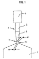
- Fig. 1 is an explanatory view showing the dislocation-free seeding method of the present invention.
- Fig. 1 is an enlarged view of the neighborhood of a seed crystal of a single crystal grown by the method of the present invention for growing a single crystal without performing necking.
- temperature of the atmosphere immediately above the silicon melt surface has a temperature gradient of about 1°C/mm within the range of 50 mm from the melt surface, and about 2°C/mm within the range of 20 mm from the melt surface, although it depends on the structure of graphite members keeping the heat in the furnace. Therefore, it was considered that, if the position of the seed crystal held immediately above the melt was deviated, the temperature of the tip end portion of the seed crystal during the heat reservation was decreased and thus the success ratio in making a crystal dislocation-free was markedly decreased. Further, it is expected that the seed crystal is not heated to a sufficiently high temperature only by heat reservation at a position above the melt surface, since the seed crystal is not brought into contact with the melt once during such heat reservation and hence there is not heat reservation by heat conduction.
- a silicon seed crystal for pulling a single crystal having a diameter of 150 mm, there was used a silicon seed crystal in a shape of square pole that a silicon seed crystal straight body had a side length of 15 mm and a tip end portion tapered into a corn shape having a vertical angle of 15°, of which surface had been etched for 200 ⁇ m or more with a mixed acid of hydrofluoric acid and nitric acid.
- the seed crystal was set on a seed crystal holder and the tip end of the seed crystal was brought into contact with a silicon melt. Then, the seed crystal was immediately pulled upwardly from a position above the silicon melt. And then, the seed crystal was sliced parallel to the length direction, and presence or absence of dislocation was investigated by X-ray topography.
- the aforementioned silicon seed crystal was first descended to a position about 20 cm above the silicon melt surface at a speed of 300 mm/min, and from that position, the seed crystal was descended at a speed of 5 mm/min to perform the operation.
- the position at which the seed crystal was brought into contact with the silicon melt was determined by applying an alternating current between the seed crystal and the silicon melt and detecting conduction.
- the investigated factors were (A) the distance between the tip end portion of the seed crystal and the silicon melt surface during heat reservation before the seed crystal is brought into contact with the silicon melt or (B) the length of the seed crystal melted in the first stage seed crystal melting step for further melting the tip end portion of the seed crystal after the tip end portion of the seed crystal is brought into contact with the silicon melt, (C) heat reservation time for heat reservation of the seed crystal before the seed crystal is brought into contact with the silicon melt or heat reservation of the seed crystal after the first stage seed crystal melting step is finished and melting is stopped, (D) melting rate of the seed crystal in the seed crystal tip end melting step after the heat reservation of the seed crystal is completed, (E) difference of the diameter M of the seed crystal tip end after the melting is completed and the minimum diameter N in a section where the diameter is increased to a desired diameter (hereinafter, also referred to as "diameter after decrease of diameter”) in the step of pulling the seed crystal after the melting of the seed crystal is completed (also referred to as diameter decreasing width), and (F
- the magnetic field intensity (F) used herein indicates a value of magnetic field intensity observed at an interface at which the tip end portion of the seed crystal and the melt surface are contacted, when a horizontal magnetic field is applied to the silicon melt in the crucible.
- FIG. 1 A state of the seed crystal during the growth of a silicon crystal pulled in the manner described above is shown in Fig. 1.
- a silicon seed crystal 1 there was used a silicon seed crystal in a shape of square pole that a silicon seed crystal straight body 2 had a side length of 15 mm and a silicon seed crystal tip end portion 3 tapered into a corn shape having a vertical angle of 15°, of which surface had been etched for 200 ⁇ m or more with a mixed acid of hydrofluoric acid and nitric acid.
- the seed crystal was set on a seed crystal holder 6 and a single crystal ingot 7 having a diameter of 150 mm was grown to investigate the success ratio in making a crystal dislocation-free.
- the aforementioned silicon seed crystal 1 was first approached to the silicon melt at a speed of 5 mm/min and the seed crystal was maintained at a position where the distance between the silicon seed crystal tip end and the silicon melt surface became A mm to perform heat reservation for C minutes, or without performing this operation, the silicon seed crystal was approached to the silicon melt at a speed of 5 mm/min so that the tip end portion of the seed crystal should be directly brought into contact with the melt surface to melt the seed crystal tip end portion for a length of B mm (B may be 0 mm), and then the melting was stopped to perform heat reservation for C minutes. Then, the tip end portion of the seed crystal is melt at a rate of D mm 3 /min.
- the diameter M of the melting completed portion 4 of the seed crystal was set to be 8 mm.
- the success ratios in making a crystal dislocation-free of the crystals in the growth of the silicon single crystals pulled as described above are shown in Table 1.
- the success ratio in making a crystal dislocation-free used herein is a value representing a ratio of the number of single crystal ingots not suffering form generation of dislocation to the number of the pulled single crystal ingots in terms of percentage.
- the present invention was explained with reference to the example in which a silicon single crystal having a diameter of 6 inches (150 mm) was grown in the aforementioned embodiment, the present invention is not limited to such a case and can be applied to a silicon single crystal having a diameter of 8 to 16 inches or more, so long as a seed crystal in a shape having a pointed tip end or a truncated pointed tip end is used and the seeding conditions according to the present invention are used to perform the seeding and pull a single crystal.
- the present invention is not limited to such a case, and a vertical magnetic field or cusp magnetic field having an effect of suppressing convection of the silicon melt can of course be used for the present invention.
Landscapes
- Chemical & Material Sciences (AREA)
- Engineering & Computer Science (AREA)
- Crystallography & Structural Chemistry (AREA)
- Materials Engineering (AREA)
- Metallurgy (AREA)
- Organic Chemistry (AREA)
- Crystals, And After-Treatments Of Crystals (AREA)
Abstract
Description

Claims (5)
- A method for producing a silicon single crystal by the Czochralski method, in which a seed crystal having a shape of a pointed tip end or a truncated pointed tip end as a shape of its tip end portion to be brought into contact with a silicon melt is used, the tip end of the seed crystal is first carefully brought into contact with the silicon melt, then the seed crystal is descended at a low speed or a surface of the silicon melt is ascended at a low speed to melt the tip end portion of the seed crystal to a desired diameter, and subsequently the seed crystal is slowly ascended or the surface of the silicon melt is slowly descended to grow a silicon single crystal ingot without performing necking, wherein after the tip end of the seed crystal is carefully brought into contact with the silicon melt, the seed crystal is maintained at that state for 5 minutes or more to reserve heat in the seed crystal.
- A method for producing a silicon single crystal by the Czochralski method, in which a seed crystal having a shape of a pointed tip end or a truncated pointed tip end as a shape of its tip end portion to be brought into contact with a silicon melt is used, the tip end of the seed crystal is first carefully brought into contact with the silicon melt, then the seed crystal is descended at a low speed or a surface of the silicon melt is ascended at a low speed to melt the tip end portion of the seed crystal to a desired diameter, and subsequently the seed crystal is slowly ascended or the surface of the silicon melt is slowly descended to grow a silicon single crystal ingot without performing necking, wherein the tip end of the seed crystal is carefully brought into contact with the silicon melt to melt the tip end portion of the seed crystal for a length of 5 mm or less, and then the seed crystal is maintained for 5 minutes or more to reserve heat in the seed crystal.
- The method for producing a silicon single crystal according to Claim 1 or 2, wherein, in the steps of melting the tip end portion of the seed crystal to a desired diameter and then slowly ascending the seed crystal or slowly descending the silicon melt surface to grow a single crystal ingot, the diameter of the crystal is decreased by 0.3 mm or more but 2 mm or less from a diameter at the time when the melting is finished and then the diameter is increased within a section of at least 3 mm from the position at which the melting of the tip end portion of the seed crystal to the desired diameter is finished.
- The method for producing a silicon single crystal according to any one of Claims 1-3, wherein, as for the rate of melting the tip end portion of the seed crystal to a desired diameter by descending the seed crystal at a low speed or ascending the silicon melt surface at a low speed, the descending speed of the seed crystal or the ascending speed of the silicon melt surface is determined as a speed changing continuously or stepwise so that the volume of the tip end portion of the seed crystal melting per minute should become 50 mm3 or less.
- The method for producing a silicon single crystal according to any one of Claims 1-4, wherein a horizontal magnetic field of 1000 G or more is applied to the melt surface in a crucible accommodating the silicon melt.
Applications Claiming Priority (3)
| Application Number | Priority Date | Filing Date | Title |
|---|---|---|---|
| JP2000049553 | 2000-02-25 | ||
| JP2000049553 | 2000-02-25 | ||
| PCT/JP2001/001224 WO2001063026A1 (en) | 2000-02-25 | 2001-02-21 | Method for producing silicon single crystal |
Publications (3)
| Publication Number | Publication Date |
|---|---|
| EP1193332A1 true EP1193332A1 (en) | 2002-04-03 |
| EP1193332A4 EP1193332A4 (en) | 2007-10-31 |
| EP1193332B1 EP1193332B1 (en) | 2009-04-22 |
Family
ID=18571477
Family Applications (1)
| Application Number | Title | Priority Date | Filing Date |
|---|---|---|---|
| EP01906146A Expired - Lifetime EP1193332B1 (en) | 2000-02-25 | 2001-02-21 | Method for producing silicon single crystal |
Country Status (7)
| Country | Link |
|---|---|
| US (1) | US6506251B1 (en) |
| EP (1) | EP1193332B1 (en) |
| JP (1) | JP4165068B2 (en) |
| KR (1) | KR100799362B1 (en) |
| DE (1) | DE60138443D1 (en) |
| TW (1) | TW546426B (en) |
| WO (1) | WO2001063026A1 (en) |
Cited By (3)
| Publication number | Priority date | Publication date | Assignee | Title |
|---|---|---|---|---|
| EP1321544A3 (en) * | 2001-12-20 | 2003-09-03 | Wacker Siltronic AG | Seed crystal for production of slicon single crystal and method for production of silicon single crystal |
| EP1498517A4 (en) * | 2002-04-24 | 2008-09-17 | Shinetsu Handotai Kk | Method for producing silicon single crystal and, silicon single crystal and silicon wafer |
| EP4428272A1 (en) * | 2023-03-10 | 2024-09-11 | Siltronic AG | Method of drawing a single crystal ingot of semiconductor material and a wafer of semiconductor material |
Families Citing this family (14)
| Publication number | Priority date | Publication date | Assignee | Title |
|---|---|---|---|---|
| US7396406B2 (en) * | 2004-02-09 | 2008-07-08 | Sumco Techxiv Corporation | Single crystal semiconductor manufacturing apparatus and method |
| JP2007223814A (en) * | 2004-02-09 | 2007-09-06 | Sumco Techxiv株式会社 | Single crystal semiconductor manufacturing method |
| EP2021279A2 (en) * | 2006-04-13 | 2009-02-11 | Cabot Corporation | Production of silicon through a closed-loop process |
| CN101148777B (en) * | 2007-07-19 | 2011-03-23 | 任丙彦 | Method and device for growing gallium-mixing silicon monocrystal by czochralski method |
| JP5083001B2 (en) * | 2008-04-08 | 2012-11-28 | 株式会社Sumco | Pulling method of silicon single crystal |
| JP4862884B2 (en) * | 2008-05-21 | 2012-01-25 | 信越半導体株式会社 | Method for producing silicon single crystal |
| JP5125983B2 (en) * | 2008-10-20 | 2013-01-23 | 信越半導体株式会社 | Method for producing silicon single crystal |
| KR101022918B1 (en) | 2009-02-18 | 2011-03-16 | 주식회사 엘지실트론 | Single crystal manufacturing method using the no-necking process |
| JP5491483B2 (en) * | 2011-11-15 | 2014-05-14 | 株式会社タムラ製作所 | Method for growing β-Ga 2 O 3 single crystal |
| JP5660020B2 (en) | 2011-12-16 | 2015-01-28 | 信越半導体株式会社 | Method for producing silicon single crystal |
| JP5805527B2 (en) * | 2011-12-28 | 2015-11-04 | グローバルウェーハズ・ジャパン株式会社 | Method for producing silicon single crystal |
| JP5756075B2 (en) | 2012-11-07 | 2015-07-29 | 株式会社タムラ製作所 | Method for growing β-Ga 2 O 3 single crystal |
| CN112567006A (en) | 2019-08-21 | 2021-03-26 | 眉山博雅新材料有限公司 | Method and apparatus for growing oxide crystal without annealing |
| CN115110146A (en) * | 2022-06-30 | 2022-09-27 | 西安奕斯伟材料科技有限公司 | Seed crystal and crystal pulling method and device |
Family Cites Families (10)
| Publication number | Priority date | Publication date | Assignee | Title |
|---|---|---|---|---|
| JPH04104988A (en) | 1990-08-20 | 1992-04-07 | Fujitsu Ltd | Growth of single crystal |
| JPH04139092A (en) | 1990-09-28 | 1992-05-13 | Fujitsu Ltd | Production of silicon single crystal and seed crystal |
| JP2937115B2 (en) * | 1996-03-15 | 1999-08-23 | 住友金属工業株式会社 | Single crystal pulling method |
| JP3387364B2 (en) | 1997-05-21 | 2003-03-17 | 信越半導体株式会社 | Silicon seed crystal, method for producing the same, and method for producing silicon single crystal using these seed crystals |
| US5885344A (en) | 1997-08-08 | 1999-03-23 | Memc Electronic Materials, Inc. | Non-dash neck method for single crystal silicon growth |
| US5932002A (en) * | 1997-08-28 | 1999-08-03 | Sumitomo Sitix Corporation | Seed crystals for pulling a single crystal and methods using the same |
| JP3267225B2 (en) * | 1997-12-26 | 2002-03-18 | 住友金属工業株式会社 | Single crystal pulling method and single crystal pulling apparatus |
| JP3402210B2 (en) * | 1997-12-27 | 2003-05-06 | 信越半導体株式会社 | Method for producing silicon single crystal |
| JP3440819B2 (en) * | 1998-04-07 | 2003-08-25 | 信越半導体株式会社 | Method for producing silicon single crystal |
| JP3065076B1 (en) * | 1999-05-13 | 2000-07-12 | 住友金属工業株式会社 | Single crystal pulling method and single crystal pulling apparatus |
-
2001
- 2001-02-21 JP JP2001561828A patent/JP4165068B2/en not_active Expired - Fee Related
- 2001-02-21 DE DE60138443T patent/DE60138443D1/en not_active Expired - Lifetime
- 2001-02-21 KR KR1020017013579A patent/KR100799362B1/en not_active Expired - Fee Related
- 2001-02-21 US US09/959,302 patent/US6506251B1/en not_active Expired - Lifetime
- 2001-02-21 EP EP01906146A patent/EP1193332B1/en not_active Expired - Lifetime
- 2001-02-21 WO PCT/JP2001/001224 patent/WO2001063026A1/en not_active Ceased
- 2001-02-23 TW TW090104216A patent/TW546426B/en not_active IP Right Cessation
Cited By (4)
| Publication number | Priority date | Publication date | Assignee | Title |
|---|---|---|---|---|
| EP1321544A3 (en) * | 2001-12-20 | 2003-09-03 | Wacker Siltronic AG | Seed crystal for production of slicon single crystal and method for production of silicon single crystal |
| EP1498517A4 (en) * | 2002-04-24 | 2008-09-17 | Shinetsu Handotai Kk | Method for producing silicon single crystal and, silicon single crystal and silicon wafer |
| EP4428272A1 (en) * | 2023-03-10 | 2024-09-11 | Siltronic AG | Method of drawing a single crystal ingot of semiconductor material and a wafer of semiconductor material |
| WO2024188617A1 (en) * | 2023-03-10 | 2024-09-19 | Siltronic Ag | Method for pulling a single crystal ingot of semiconductor material, and wafer of semiconductor material |
Also Published As
| Publication number | Publication date |
|---|---|
| JP4165068B2 (en) | 2008-10-15 |
| US6506251B1 (en) | 2003-01-14 |
| KR20020006710A (en) | 2002-01-24 |
| WO2001063026A1 (en) | 2001-08-30 |
| TW546426B (en) | 2003-08-11 |
| DE60138443D1 (en) | 2009-06-04 |
| KR100799362B1 (en) | 2008-01-30 |
| EP1193332B1 (en) | 2009-04-22 |
| EP1193332A4 (en) | 2007-10-31 |
Similar Documents
| Publication | Publication Date | Title |
|---|---|---|
| EP1193332B1 (en) | Method for producing silicon single crystal | |
| US5911822A (en) | Method of manufacturing silicon monocrystal, and seed crystal used in the method | |
| US6869477B2 (en) | Controlled neck growth process for single crystal silicon | |
| JPWO2001063026A1 (en) | Silicon single crystal manufacturing method | |
| JP2937115B2 (en) | Single crystal pulling method | |
| JP2973917B2 (en) | Single crystal pulling method | |
| EP0949361A2 (en) | Silicon seed crystal for the Czochralski method and method for producing a silicon single crystal | |
| US9476142B2 (en) | Method for manufacturing silicon single crystal | |
| WO2001063022A2 (en) | Controlled neck growth process for single crystal silicon | |
| EP0930381B1 (en) | Method of producing a silicon monocrystal | |
| JPH09249492A (en) | Seed crystal for pulling single crystal and method for pulling single crystal using the seed crystal | |
| JPH09235186A (en) | Seed crystal for pulling single crystal and method for pulling single crystal using the seed crystal | |
| JP3402210B2 (en) | Method for producing silicon single crystal | |
| EP0949359B1 (en) | Process for producing a silicon single crystal by Czochralski method | |
| JPH04139092A (en) | Production of silicon single crystal and seed crystal | |
| US6171392B1 (en) | Method for producing silicon single crystal | |
| JP3473477B2 (en) | Method for producing silicon single crystal | |
| JPH09249495A (en) | Seed crystal for pulling single crystal and method for pulling single crystal using the seed crystal | |
| JPH11209197A (en) | Production of silicon single crystal | |
| JPH11322492A (en) | Production of silicon single crystal | |
| JPH09249493A (en) | Seed crystal for pulling single crystal and method for pulling single crystal using the seed crystal | |
| JPH09227279A (en) | Single crystal growth method | |
| JPH09227280A (en) | Single crystal growth method | |
| JP2005281018A (en) | Silicon single crystal pulling method | |
| JP2006069874A (en) | Method for producing silicon single crystal |
Legal Events
| Date | Code | Title | Description |
|---|---|---|---|
| PUAI | Public reference made under article 153(3) epc to a published international application that has entered the european phase |
Free format text: ORIGINAL CODE: 0009012 |
|
| 17P | Request for examination filed |
Effective date: 20011108 |
|
| AK | Designated contracting states |
Kind code of ref document: A1 Designated state(s): AT BE CH CY DE DK ES FI FR GB GR IE IT LI LU MC NL PT SE TR |
|
| AX | Request for extension of the european patent |
Free format text: AL;LT;LV;MK;RO;SI |
|
| RBV | Designated contracting states (corrected) |
Designated state(s): DE |
|
| A4 | Supplementary search report drawn up and despatched |
Effective date: 20071004 |
|
| 17Q | First examination report despatched |
Effective date: 20080205 |
|
| GRAP | Despatch of communication of intention to grant a patent |
Free format text: ORIGINAL CODE: EPIDOSNIGR1 |
|
| GRAP | Despatch of communication of intention to grant a patent |
Free format text: ORIGINAL CODE: EPIDOSNIGR1 |
|
| RIC1 | Information provided on ipc code assigned before grant |
Ipc: C30B 29/06 20060101AFI20081010BHEP Ipc: C30B 15/36 20060101ALI20081010BHEP |
|
| GRAS | Grant fee paid |
Free format text: ORIGINAL CODE: EPIDOSNIGR3 |
|
| GRAA | (expected) grant |
Free format text: ORIGINAL CODE: 0009210 |
|
| RAP1 | Party data changed (applicant data changed or rights of an application transferred) |
Owner name: SHIN-ETSU HANDOTAI CO., LTD. |
|
| AK | Designated contracting states |
Kind code of ref document: B1 Designated state(s): DE |
|
| REF | Corresponds to: |
Ref document number: 60138443 Country of ref document: DE Date of ref document: 20090604 Kind code of ref document: P |
|
| PLBE | No opposition filed within time limit |
Free format text: ORIGINAL CODE: 0009261 |
|
| STAA | Information on the status of an ep patent application or granted ep patent |
Free format text: STATUS: NO OPPOSITION FILED WITHIN TIME LIMIT |
|
| 26N | No opposition filed |
Effective date: 20100125 |
|
| PGFP | Annual fee paid to national office [announced via postgrant information from national office to epo] |
Ref country code: DE Payment date: 20200211 Year of fee payment: 20 |
|
| REG | Reference to a national code |
Ref country code: DE Ref legal event code: R071 Ref document number: 60138443 Country of ref document: DE |