EP1191686A2 - Method and circuit for controlling baseband gain - Google Patents
Method and circuit for controlling baseband gain Download PDFInfo
- Publication number
- EP1191686A2 EP1191686A2 EP01121259A EP01121259A EP1191686A2 EP 1191686 A2 EP1191686 A2 EP 1191686A2 EP 01121259 A EP01121259 A EP 01121259A EP 01121259 A EP01121259 A EP 01121259A EP 1191686 A2 EP1191686 A2 EP 1191686A2
- Authority
- EP
- European Patent Office
- Prior art keywords
- gain
- prescribed
- output
- input
- baseband
- Prior art date
- Legal status (The legal status is an assumption and is not a legal conclusion. Google has not performed a legal analysis and makes no representation as to the accuracy of the status listed.)
- Granted
Links
Images





Classifications
-
- H—ELECTRICITY
- H03—ELECTRONIC CIRCUITRY
- H03G—CONTROL OF AMPLIFICATION
- H03G3/00—Gain control in amplifiers or frequency changers
-
- H—ELECTRICITY
- H03—ELECTRONIC CIRCUITRY
- H03G—CONTROL OF AMPLIFICATION
- H03G1/00—Details of arrangements for controlling amplification
- H03G1/0005—Circuits characterised by the type of controlling devices operated by a controlling current or voltage signal
- H03G1/0088—Circuits characterised by the type of controlling devices operated by a controlling current or voltage signal using discontinuously variable devices, e.g. switch-operated
-
- H—ELECTRICITY
- H03—ELECTRONIC CIRCUITRY
- H03G—CONTROL OF AMPLIFICATION
- H03G3/00—Gain control in amplifiers or frequency changers
- H03G3/20—Automatic control
- H03G3/30—Automatic control in amplifiers having semiconductor devices
- H03G3/3052—Automatic control in amplifiers having semiconductor devices in bandpass amplifiers (H.F. or I.F.) or in frequency-changers used in a (super)heterodyne receiver
- H03G3/3068—Circuits generating control signals for both R.F. and I.F. stages
Definitions
- the present invention relates to a baseband gain control and particularly to a baseband gain control method and circuit capable of effectively preventing problems derived from a DC offset in the gain control of a direct conversion baseband circuit or the like.
- a receiver utilizing direct conversion is advantageous over conventional super-heterodyne type receiver in the following respects and, therefore, expected to be widely used in the future:
- FIG. 6 is a view showing the concrete constitution of a direct conversion receiver.
- FIG. 6 shows a baseband gain control system for controlling the gain of a direct conversion baseband circuit, e.g., a system which has a wide dynamic range in the reception signals of a receiver of such a type as W-CDMA (Wide Band Code Division Multiple Access).
- W-CDMA Wide Band Code Division Multiple Access
- a high frequency signal received by an antenna 201 is subjected to band-limitation by a high frequency band-pass filter 202 and a received band is taken out.
- the signal thus band-limited is amplified by a low noise amplifier LNA 203 and directly inputted into a quadrature demodulator 204.
- the quadrature demodulator 204 is driven by a local signal generated by a local oscillator 225.
- the frequency of this local signal is the same as the central frequency of the received high frequency signal.
- the quadrature demodulator 204 consists of multiplication circuits 222 and 223 and a phase circuit 224.
- the balanced outputs of the low noise amplifier LNA 203 are multiplied by the multiplication circuits 222 and 223 through an amplifier 221 in response to the balanced outputs of an orthogonal signal having a phase of 0° and that of 90° of the local signal, respectively, a baseband signal is directly generated from the high frequency signal, and two types of signals, i.e., baseband signals I and Q, are outputted as demodulated outputs.
- baseband signals I and Q are subjected to band-limitation by baseband filters 205 and 206, respectively, and then amplified by an AGC circuit 207 so as to have a constant average amplitude.
- the dynamic range of the AGC circuit 207 has characteristics of reaching several tens of decibels (about 80dB for CDMA).
- the outputs of the AGC circuit 207 are outputted to the next stage as signals 215 and 216, respectively. It is noted that a circuit controlling the gain of this circuit and the algorithm thereof are unrelated to the present invention and, therefore, not described herein.
- channel filters for suppressing adjacent channels are realized not by SAW filters for an IF band but by the baseband filters 205 and 206. Since they can be realized by circuits using active elements, the baseband filters 205 and 206 are suited for an IC.
- the high frequency signal is directly converted into the baseband signals, there is no need to provide a second local oscillator. For these reasons, there is a probability that all the reception circuits from the low noise amplifier LNA 203 to the baseband outputs can be realized by one chip. This greatly contributes to making a cellular phone smaller in size and to the reduction of the number of parts.
- the gain of the AGC sometimes becomes as high as 80 dB and a saturation phenomenon occurs that outputs are fixed to a power supply or the ground.
- a DC offset of 1mV in the bandpass filter 205 and the gain of the AGC circuit 207 is 80 dB, i.e., 10,000 times as high as an input, a DC component of 10 V is outputted. Needless to say, such a voltage is far beyond the voltage of a battery for a cellular phone, with the result that the cellular phone cannot operate.
- C-cut high-pass filters
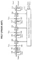
- FIG. 7 is a view showing that the baseband circuit for I or Q shown in FIG. 6 is taken out.
- the baseband circuit consists of a plurality of gain control amplifiers having C-cut structures. To simplify description, FIG. 7 shows the baseband circuit as a single-end circuit.
- a baseband filter 101 and variable gain amplifiers 102, 103 and 104 (which amplifiers may be also referred to as "VGA1", “VGA2” and “VGA3", respectively) correspond to the baseband filter 205 (206) and the variable gain amplifiers 208 (211), 209 (212) and 210 (213), respectively.
- high-pass filters 109 to 111 corresponding to C-cuts are inserted between the input section of the circuit and the VGA 102, the VGA 102 and VGA 103, the VGA 103 and the VGA 104 and the VGA 104 and the output section, respectively.
- the gains of the VGA 1, VGA2 and VGA 3 are controlled by gain control data distributed from the gain distribution circuit 112 based on gain data inputted from externally.
- the high-pass filters into the baseband circuit in appropriate units of the circuit, the propagation of a direct current is prevented in a static state in which gains have no change.
- the saturation of a signal due to the DC offset can be prevented.
- the gains of the VGA1, VGA2 and VGA3 are g 1 , g 2 and g 3 , respectively, and that these gains are changed to g 1 ', g 2 ' and g 3 ', respectively.
- the following conditions are set:
- V out ( t ) ( g 3 ' - g 3 ) ⁇ V of 3 ⁇ e - ⁇ t
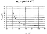
- FIG. 8 shows the waveform of the mathematical expression (4) if the offset voltage V of3 is 1 mV and the gain g 3 is changed from 1 time to 16 times as high as the input.
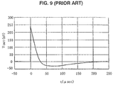
- FIG. 9 shows the waveform of the mathematical expression (7) if the offset voltage V of2 is 1 mV and the gain g 3 is 16 times as high as the input and the gain g 2 is changed from 1 time to 16 times as high as the input.
- FIG. 10 shows the waveform of the mathematical expression (10) if the offset voltage V of1 is 1 mV, the gains g 3 and g 2 are 16 times as high as the inputs and the gain g 1 is changed from 1 time to 16 times as high as the input.
- the 3dB-cutoff frequency of each high-pass filter is 5 kH z and the value of ⁇ is 31415.93.
- An object of the present invention is to provide a baseband gain control method and circuit capable of suppressing the generation of a transient voltage in the setting of the gains of a plurality of variable gain amplifiers in a baseband circuit.
- the present invention is directed to control a baseband gain by setting gains of a plurality of variable gain amplifiers amplifying a baseband signal and connected to one another in series, to decrease the generation of a voltage due to a transient phenomenon.
- the settings of the gains of the plurality of variable gain amplifiers in the baseband circuit are controlled as follows:
- gain control is carried out so that the upper limit of the quantity of the change of the gains of a plurality of variable gain amplifiers for a baseband signal is set. Further, if the gain is to be increased, the gains of the variable gain amplifiers starting at the variable gain amplifier close to an input are sequentially increased. Further, if the gain is to be decreased, the gains of the variable gain amplifiers starting at the variable gain amplifier farthest to the input are sequentially decreased. Thus, it is possible to effectively suppress the generation of a transient voltage caused by a DC offset during the gain control.
- the combination of the gain control for providing the upper limit of the quantity of the change of a gain and the distribution control for distributing different gains to a plurality of variable gain amplifiers according to the increase and decrease of the gain enables, in particular, suppressing the generation of a transient voltage caused by a DC offset more effectively.
- the present invention is applied to the gain control of a direct conversion baseband circuit, e.g., the baseband gain control of a direct conversion baseband circuit having a wide dynamic range of a reception signal such as a receiver of a W-CDMA (Wide Band Code Division Multiple Access) type, the present invention exhibits considerably great advantage.
- a direct conversion baseband circuit e.g., the baseband gain control of a direct conversion baseband circuit having a wide dynamic range of a reception signal such as a receiver of a W-CDMA (Wide Band Code Division Multiple Access) type
- W-CDMA Wide Band Code Division Multiple Access
- FIG. 1 is a view showing one mode for carrying out a baseband gain control circuit of the present invention.
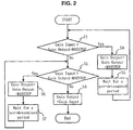
- FIG. 2 is a flow chart showing the operation of a gain converting circuit in this mode for carrying out the invention.
- FIG. 3 shows a manner in which the gain of a variable gain amplifier follows gain control data.
- FIG. 4 is a flow chart showing the operation of a gain distribution circuit.
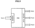
- FIG. 5 is a view showing an example in which the gain distribution circuit is constituted out of an ROM.
- FIG. 6 is a view showing the constitution of a conventional direct conversion receiver.
- FIG. 7 is a view showing the baseband circuit of the circuit shown in FIG. 6 as a single-end circuit for brevity.
- FIG. 8 shows the waveform of an expression (4) if V of3 is 1 mV and g 3 is changed from 1 time to 16 times as high as an input.
- FIG. 9 shows the waveform of an expression (7) if V of2 is 1 mV and g 3 is 16 times as high as the input and g 2 is changed from 1 time to 16 times as high as the input.
- FIG. 10 shows the waveform of an expression (10) if V of1 is 1 mV and g 3 and g 2 are 16 times as high as the input and g 1 is changed from 1 time to 16 times as high as the input.
- FIG. 1 is a block diagram showing the basic constitution of a baseband gain control circuit of the present invention.
- a signal path shown therein has, similarly to the conventional circuit shown in FIG. 7, a constitution of the reception signal baseband gain control system of a receiver such as a W-CDMA (Wide Band Code Division Multiple Access) system.
- the block diagram of FIG. 1 shows a single-end circuit as in the case of the description of the conventional circuit.
- the first mode for carrying out the present invention is characterized by comprising a gain distribution circuit 112 and a gain converting circuit 113 as shown in FIG. 1 and in that an upper limit of the gain control is set to the gain control circuit 113.
- the gain converting circuit 113 is a circuit converting inputted gain data (Gain Data: corresponding to dB) into gain output data (Gain Output: corresponding to dB) actually set to variable gain amplifiers.
- the gain distribution circuit 112 is a circuit having a function of distributing the gain output data inputted from the gain converting circuit 113 to a plurality of variable gain amplifiers as gain control data and controlling the data.
- the circuit is constituted so that that the gain output data (Gain Output), either as it is or uniformly amplified/attenuated, is distributed and supplied to a plurality of variable gain amplifiers.
- the Gain Input has a large change, e.g., 48 dB is changed by 24 dB to 72 dB and this change is reflected on the set values of the variable gain amplifiers, respectively, a high transient voltage is generated by a DC offset as already described in detail in "Problems that the Invention is to Solve" part.
- the upper limit or the maximum step of a gain (MAXSTEP) which can be changed once is set.
- MAXSTEP is set at 2 dB.
- the quantity of the change of a gain of 24 dB is attained from 12 quantities of change each of 2 dB at intervals of pre-determined periods (Pre-Determined Periods).
- FIG. 8 shows the transient voltage if V of3 is 1 mV and the gain g 3 of the VGA3 is changed from 1 times (0 dB) to 16 times (24 dB) as high as the input.
- the transient voltage at a peak of 1 mV ⁇ (16-1) 15 mV is generated.
- the gain converting circuit 113 outputs such gain output data, as gain set value, to the gain distribution circuit 112 and the gain distribution circuit 112 distributes the gain set value to the respective variable gain amplifiers 102, 103 and 104 either as it is or while amplifying/attenuating the value.
- the gains of the respective variable gain amplifiers are controlled a plurality of times at intervals of pre-determined periods based on the upper limit of the maximum quantity of change or MAXSTEP, whereby the peak value of a transient voltage can be greatly reduced.
- FIG. 2 is a flow chart showing the operation of the gain converting circuit 113 in the first mode for carrying out the invention. If the inputted Gain Input value is higher than the Gain Output currently set to the variable gain amplifiers by MAXSTEP dB or more ('YES' in a step s1), then the MAXSTEP dB is added to the currently set Gain Output to obtain a newly set Gain Output (in a step s4).
- the quantity of the change of the Gain Output in each pre-determined period is limited to MAXSTEP dB or lower.
- FIG. 3 shows a manner in which the Gain Output follows the Gain Input.
- the Gain Input and the Gain Output satisfy Gain Input ⁇ Gain Output + MAXSTEP. In this case, they also satisfy Gain Input ⁇ Gain Output - MAXSTEP.
- control is carried out for attaining a required gain change as a plurality of times of changes of the gain each equal to or lower than the limiting value of the gain change. That is, a plurality of quantities of the change of the gain and the quantity of the change of the last gain equal to or lower than the limit value are controlled.
- the gain control in this mode for carrying out the invention therefore, even if the Gain Input is greatly changed, the change of a gain is gradually made for a long period of time and the change of the Gain Output can be, therefore, decreased. Due to this, even if there is an offset in a plurality of variable gain amplifiers, it is possible to suppress the generation of a sudden transient voltage.
- the gain distribution circuit 112 exercises control so as to supply different gain control data to a plurality of variable gain amplifiers.
- the gain converting circuit 113 outputs gain data as gain control data as it is.
- the gain distribution circuit distributes a gain as follows.
- the gains of all the VGA's provided right of the VGA x are set at a minimum gain, respectively.
- the minimum gain is 0 dB.
- FIG. 4 is a flow chart showing the operation of the gain distribution circuit 112 in the second mode for carrying out the invention.
- a control algorithm that the gains of variable gain amplifiers starting at a variable gain amplifier close to an input are sequentially increased and that, if the gain is decreased, the gains of variable gain amplifiers starting at a variable gain amplifier farthest to the input are sequentially decreased is utilized.
- the gain distribution circuit 112 exercises control so that the maximum value of the amplification gains of the variable gain amplifiers in this mode becomes, for example, 24 dB, threshold values are set at 24 dB and 48 dB for the input gain data (Gain) of the gain distribution circuit and that the respective variable gain amplifiers have different gains according to the state of the input gain data.
- a step s11 it is judged whether or not the Gain inputted to the gain distribution circuit 112 is higher than 48 dB. If the Gain is higher than 48 dB, then the VGA1, VGA2 and VGA 3 are set at 24 dB, 24 dB and (Gain-48 dB), respectively and the operation returns to the step s11. If it is judged that the Gain is equal to or lower than 48 dB in the step s11, it is then judged whether or not the Gain is higher than 24 dB in a step s12.
- the VGA1, VGA2 and VGA3 are set at 24 dB, (Gain-24 dB) and 0 dB, respectively and the operation returns to the processing of the step s11. If the Gain is lower than 24 dB, then the VGA1, VGA2 and VGA3 are set at Gain, 0 dB and 0dB, respectively and the operation returns to the processing of the step s11.
- VGA1, VGA2 and VGA3 are distributed to the VGA1, VGA2 and VGA3 as the respective gain control data of a plurality of variable gain control amplifiers as shown in FIG. 4 and a certain VGA is changed, data is controlled so that the gains of the VGA's on the output side relative to the certain VGA become a minimum gain, respectively.
- variable gain amplifiers starting from the variable gain amplifier close to an input are sequentially increased. If the gain is to be decreased, those of variable gain amplifiers starting from the variable gain amplifier farthest to the input are sequentially decreased.
- the first mode and the second mode for carrying out the invention are combined.
- a combination of gain control while setting an upper limit for the quantity of gain change and distribution control for distributing different gains to a plurality of variable gain amplifiers according to the increase and decrease of the gain are conducted, thereby making it possible to realize the effect of suppressing a transient voltage in a multiplied manner.
- a gain converting circuit 113 is constituted to carry out an operation with a maximum step provided at the circuit 113 as in the case of the first mode for carrying out the invention.
- a gain distribution circuit 112 is constituted to distribute gain control data as in the case of the second mode for carrying out the invention.
- a gain distribution circuit 112 can be constituted out of an ROM while the basic constitution of the circuit is the same as those described above.
- FIG. 5 shows an example in which the gain distribution circuit is constituted out of an ROM.
- the gains of respective variable gain amplifiers corresponding to the address input are read from the ROM and thereby set.
- Data written to the ROM is pre-determined so as to satisfy the algorithm of FIG. 4, whereby the gain distribution circuit can operate in the same manner as that in the preceding modes for carrying out the invention.
Landscapes
- Control Of Amplification And Gain Control (AREA)
- Transmitters (AREA)
Abstract
Description
Claims (9)
- A gain control method for maintaining a total amplifying gain of an output from a baseband amplifier including series-connected variable gain amplifiers (VGAs), by using a prescribed gain limit and a prescribed time period, which comprising the steps of:fixing a prescribed gain for said output from said baseband amplifyier;comparing said total amplifying gain with said prescribed gain;adding said prescribed gain limit to said prescribed gain when said total amplifying gain is higher than said prescribed gain by said prescribed gain limit or more, or subtracting said prescribed gain limit from said prescribed gain when said total amplifying gain is lower than said prescribed gain by said prescribed gain limit or more; andrepeating the adding step or the subtracting step until said total amplifying gain becomes equal to said prescribed gain.
- The gain control method according to claim 1, wherein the repeating step is limited to a prescribed number.
- The gain control method according to claim 1, wherein said prescribed gain is distributed in such a manner that the gains of said VGAs are increased in serial order from the input to the output of said baseband amplifier when said total amplifying gain is to be increased, while the gains of the VGAs are decreased in serial order from the output to the input of said baseband amplifier when said total amplifying gain is to be decreased.
- A gain control method for maintaining a total amplifying gain of an output from a baseband amplifier including series-connected variable gain amplifiers (VGAs), by using a prescribed gain limit and a prescribed time period, comprising the steps of:fixing a prescribed gain for said output from said baseband amplifyier;comparing said total amplifying gain with said prescribed gain;distributing said prescribed gain in such a manner that the gains of said VGAs are increased in serial order from the input to the output of said baseband amplifier when said total amplifying gain is to be increased, while the gains of the VGAs are decreased in serial order from the output to the input of said baseband amplifier when said total amplifying gain is to be decreased.
- A baseband amplifier including series-connected variable gain amplifiers (VGA) for maintaining a total amplifying gain, which comprises :a gain converting circuit for fixing a prescribed gain for the output from said baseband amplifyier; for comparing said total amplifying gain with said prescribed gain; for adding a prescribed gain limit to said prescribed gain when said total amplifying gain is higher than said prescribed gain by said prescribed gain limit or more, or subtracting said prescribed gain limit from said prescribed gain when said total amplifying gain is lower than said prescribed gain by said prescribed gain limit or more; and for repeating the adding step or the subtracting step until said total amplifying gain becomes equal to said prescribed gain; anda gain distribution circuit for distributing the output from said gain converting circuit.
- The baseband amplifier according to claim 5, wherein said output from said gain converting circuit is equally distributed to said VGAs.
- The baseband amplifier according to claim 5, wherein the repeating step is limited to a prescribed number.
- The baseband amplifier according to claim 5, wherein said gain distribution circuit distributes said prescribed gain in such a manner that the gains of said VGAs are increased in serial order from the input to the output of said baseband amplifier when said total amplifying gain is to be increased, while the gains of the VGAs are decreased in serial order from the output to the input of said baseband amplifier when said total amplifying gain is to be decreased.
- A baseband amplifier including series-connected variable gain amplifiers (VGA) for maintaining a total amplifying gain, which comprisesa gain converting circuit for fixing a prescribed gain for the output from said baseband amplifyier and for comparing said total amplifying gain with said prescribed gain; anda gain distribution circuit for distributing said prescribed gain in such a manner that the gains of said VGAs are increased in serial order from the input to the output of said baseband amplifier when said total amplifying gain is to be increased, while the gains of the VGAs are decreased in serial order from the output to the input of said baseband amplifier when said total amplifying gain is to be decreased.
Priority Applications (1)
| Application Number | Priority Date | Filing Date | Title |
|---|---|---|---|
| EP09152894A EP2071720A1 (en) | 2000-09-13 | 2001-09-05 | Method and circuit for controlling baseband gain |
Applications Claiming Priority (2)
| Application Number | Priority Date | Filing Date | Title |
|---|---|---|---|
| JP2000278334 | 2000-09-13 | ||
| JP2000278334A JP3479835B2 (en) | 2000-09-13 | 2000-09-13 | Baseband gain control method and baseband gain control circuit |
Related Child Applications (2)
| Application Number | Title | Priority Date | Filing Date |
|---|---|---|---|
| EP09152894A Division-Into EP2071720A1 (en) | 2000-09-13 | 2001-09-05 | Method and circuit for controlling baseband gain |
| EP09152894A Division EP2071720A1 (en) | 2000-09-13 | 2001-09-05 | Method and circuit for controlling baseband gain |
Publications (3)
| Publication Number | Publication Date |
|---|---|
| EP1191686A2 true EP1191686A2 (en) | 2002-03-27 |
| EP1191686A3 EP1191686A3 (en) | 2004-09-01 |
| EP1191686B1 EP1191686B1 (en) | 2014-05-14 |
Family
ID=18763517
Family Applications (2)
| Application Number | Title | Priority Date | Filing Date |
|---|---|---|---|
| EP09152894A Withdrawn EP2071720A1 (en) | 2000-09-13 | 2001-09-05 | Method and circuit for controlling baseband gain |
| EP01121259.4A Expired - Lifetime EP1191686B1 (en) | 2000-09-13 | 2001-09-05 | Method and circuit for controlling baseband gain |
Family Applications Before (1)
| Application Number | Title | Priority Date | Filing Date |
|---|---|---|---|
| EP09152894A Withdrawn EP2071720A1 (en) | 2000-09-13 | 2001-09-05 | Method and circuit for controlling baseband gain |
Country Status (5)
| Country | Link |
|---|---|
| US (1) | US6480063B2 (en) |
| EP (2) | EP2071720A1 (en) |
| JP (1) | JP3479835B2 (en) |
| KR (1) | KR100462428B1 (en) |
| CN (1) | CN1168206C (en) |
Cited By (2)
| Publication number | Priority date | Publication date | Assignee | Title |
|---|---|---|---|---|
| EP1712000A4 (en) * | 2003-09-12 | 2007-03-28 | Zarbana Digital Fund Llc | Staggered agc with digitally controlled vga |
| WO2008057868A3 (en) * | 2006-11-07 | 2008-12-11 | Microtune Texas Lp | Pseudo digital gain control for broadband tuner |
Families Citing this family (20)
| Publication number | Priority date | Publication date | Assignee | Title |
|---|---|---|---|---|
| US6826388B1 (en) * | 1999-11-15 | 2004-11-30 | Renesas Technology Corp. | Mobile communication apparatus including dividers in transmitter and receiver |
| US6498927B2 (en) * | 2001-03-28 | 2002-12-24 | Gct Semiconductor, Inc. | Automatic gain control method for highly integrated communication receiver |
| GB0127535D0 (en) * | 2001-11-16 | 2002-01-09 | Hitachi Ltd | A communication semiconductor integrated circuit device and wireless communication system |
| US7212586B2 (en) * | 2002-01-18 | 2007-05-01 | Broadcom Corporation | Direct conversion RF transceiver for wireless communications |
| US7257383B2 (en) * | 2004-03-08 | 2007-08-14 | Broadcom Corporation | Method and system for improving dynamic range for communication systems using upstream analog information |
| US7545888B2 (en) | 2004-04-09 | 2009-06-09 | Micronas Semiconductors, Inc. | Apparatus for and method of controlling a digital demodulator coupled to an equalizer |
| WO2006020950A1 (en) * | 2004-08-12 | 2006-02-23 | Micronas Semiconductors, Inc. | Automatic gain control unit of a receiver |
| CN100568749C (en) * | 2004-08-18 | 2009-12-09 | 罗姆股份有限公司 | Discrimination circuit, signal processing circuit, and electronic apparatus |
| US7154335B2 (en) * | 2004-09-29 | 2006-12-26 | Intel Corporation | Variable gain amplifier with direct current offset correction |
| CN100382439C (en) * | 2004-12-02 | 2008-04-16 | 大唐移动通信设备有限公司 | Self interference signal clearing method for direct frequency conversion receiver |
| JP4227599B2 (en) | 2005-04-12 | 2009-02-18 | パナソニック株式会社 | Receiver circuit |
| DE602005015438D1 (en) * | 2005-08-04 | 2009-08-27 | Dibcom | Method and apparatus for automatic low jitter control |
| JP4912660B2 (en) * | 2005-10-19 | 2012-04-11 | 株式会社トプコン | Level detector |
| US7805117B2 (en) * | 2006-02-28 | 2010-09-28 | Motorola, Inc. | Method and apparatus for minimizing noise in a transmitter |
| CN101162925B (en) * | 2006-10-11 | 2011-10-26 | 中兴通讯股份有限公司 | Switch adjusting method of gain device in automatic gain control device |
| KR100823687B1 (en) | 2006-10-12 | 2008-04-18 | 삼성전기주식회사 | Variable gain amplifier and its gain control method |
| WO2011039791A1 (en) * | 2009-09-29 | 2011-04-07 | 株式会社 東芝 | Receiver |
| US8433274B2 (en) * | 2010-03-19 | 2013-04-30 | SiTune Corporation | Dynamic gain assignment in analog baseband circuits |
| KR102219849B1 (en) * | 2014-01-03 | 2021-02-24 | 삼성전자주식회사 | Apparatus and method for calibration of a direct current offset in a direct conversion receiver |
| US10608600B2 (en) | 2015-12-23 | 2020-03-31 | Analog Devices, Inc | Adaptable receiver amplifier |
Family Cites Families (12)
| Publication number | Priority date | Publication date | Assignee | Title |
|---|---|---|---|---|
| US5023569A (en) * | 1989-06-29 | 1991-06-11 | Motorola, Inc. | Variable gain amplifier |
| JPH05275946A (en) * | 1992-03-30 | 1993-10-22 | Mitsubishi Electric Corp | Gain control amplifier |
| WO1993026094A1 (en) * | 1992-06-08 | 1993-12-23 | Motorola, Inc. | Receiver automatic gain control |
| DE59508874D1 (en) * | 1994-07-08 | 2001-01-04 | Infineon Technologies Ag | Amplifier arrangement and receiver circuit containing the amplifier arrangement |
| JP3139734B2 (en) * | 1995-11-07 | 2001-03-05 | 日本電気株式会社 | Variable gain amplifier |
| JP2996170B2 (en) * | 1996-03-21 | 1999-12-27 | 日本電気株式会社 | Gain control circuit |
| US6006079A (en) * | 1997-06-13 | 1999-12-21 | Motorola, Inc. | Radio having a fast adapting direct conversion receiver |
| WO1999043083A1 (en) * | 1998-02-19 | 1999-08-26 | Ntt Mobile Communications Network Inc. | Amplifier for radio transmission |
| JP3986161B2 (en) | 1998-06-02 | 2007-10-03 | 富士通株式会社 | Driver circuit for signal transmission |
| US6107878A (en) * | 1998-08-06 | 2000-08-22 | Qualcomm Incorporated | Automatic gain control circuit for controlling multiple variable gain amplifier stages while estimating received signal power |
| US6353364B1 (en) * | 1998-12-22 | 2002-03-05 | Ericsson Inc. | Digitally gain controllable amplifiers with analog gain control input, on-chip decoder and programmable gain distribution |
| JP3739614B2 (en) * | 1999-11-24 | 2006-01-25 | アルプス電気株式会社 | Transmitter for output power adjustment |
-
2000
- 2000-09-13 JP JP2000278334A patent/JP3479835B2/en not_active Expired - Fee Related
-
2001
- 2001-09-05 EP EP09152894A patent/EP2071720A1/en not_active Withdrawn
- 2001-09-05 EP EP01121259.4A patent/EP1191686B1/en not_active Expired - Lifetime
- 2001-09-13 KR KR10-2001-0056476A patent/KR100462428B1/en not_active Expired - Fee Related
- 2001-09-13 CN CNB011421282A patent/CN1168206C/en not_active Expired - Fee Related
- 2001-09-13 US US09/950,751 patent/US6480063B2/en not_active Expired - Lifetime
Cited By (5)
| Publication number | Priority date | Publication date | Assignee | Title |
|---|---|---|---|---|
| EP1712000A4 (en) * | 2003-09-12 | 2007-03-28 | Zarbana Digital Fund Llc | Staggered agc with digitally controlled vga |
| US7433431B2 (en) | 2003-09-12 | 2008-10-07 | Zarbana Digital Fund, Llc | Staggered AGC with digitally controlled VGA |
| WO2008057868A3 (en) * | 2006-11-07 | 2008-12-11 | Microtune Texas Lp | Pseudo digital gain control for broadband tuner |
| US8184206B2 (en) | 2006-11-07 | 2012-05-22 | Csr Technology Inc. | Pseudo digital gain control for broadband tuner |
| US8786784B2 (en) | 2006-11-07 | 2014-07-22 | CSR Technology, Inc. | Pseudo digital gain control for broadband tuner |
Also Published As
| Publication number | Publication date |
|---|---|
| EP1191686B1 (en) | 2014-05-14 |
| EP1191686A3 (en) | 2004-09-01 |
| US6480063B2 (en) | 2002-11-12 |
| CN1344062A (en) | 2002-04-10 |
| EP2071720A1 (en) | 2009-06-17 |
| US20020047744A1 (en) | 2002-04-25 |
| KR20020021075A (en) | 2002-03-18 |
| JP3479835B2 (en) | 2003-12-15 |
| CN1168206C (en) | 2004-09-22 |
| KR100462428B1 (en) | 2004-12-17 |
| JP2002094344A (en) | 2002-03-29 |
Similar Documents
| Publication | Publication Date | Title |
|---|---|---|
| EP1191686A2 (en) | Method and circuit for controlling baseband gain | |
| EP3291451B1 (en) | Receiver and wireless communications apparatus | |
| JP3489621B2 (en) | Baseband circuit of direct conversion receiver | |
| US20030142767A1 (en) | Base band circuit of receiver and low cut-off frequency control method | |
| WO2021115453A1 (en) | Wireless receiver and wireless device | |
| JP2996170B2 (en) | Gain control circuit | |
| JP2009124189A (en) | Automatic gain control circuit | |
| US6775336B1 (en) | Receiver and gain control method of the same | |
| KR100968807B1 (en) | Variable Gain Amplifiers and Receivers Comprising the Same | |
| EP1538745B1 (en) | A mobile communication terminal apparatus, a variable gain amplifier circuit and a gain control circuit | |
| US7856216B2 (en) | Diversity receiver and gain adjusting method therefor | |
| US9413320B1 (en) | Programmable broad bandwidth gain amplifier | |
| US5875390A (en) | Programmable intermediate frequency RSSI system including an adjustable rectifying stage | |
| KR20030047111A (en) | Apparatus and method for keeping linearity of radio frequency receiver block in mobile communication system | |
| US20050135520A1 (en) | Multi-branch radio frequency amplifying apparatus and method | |
| KR101768358B1 (en) | High-Efficiency High-Integrated Receiver | |
| CN217335929U (en) | AGC realization circuit based on multi-level output signal strength detection and communication system | |
| RU2715406C1 (en) | Input linear module of broadband receiving microwave device with extended dynamic range | |
| US9866179B1 (en) | Multipath linear low noise amplifier | |
| JP2000174650A (en) | Receiver gain control method | |
| JP2769563B2 (en) | Logarithmic amplifier | |
| KR20020021012A (en) | Amplification device with optimized linearity | |
| JP2522432Y2 (en) | FM receiver | |
| JPH1155138A (en) | Receiver | |
| JP2001189667A (en) | Transmission power control circuit and transmission power control method |
Legal Events
| Date | Code | Title | Description |
|---|---|---|---|
| PUAI | Public reference made under article 153(3) epc to a published international application that has entered the european phase |
Free format text: ORIGINAL CODE: 0009012 |
|
| AK | Designated contracting states |
Kind code of ref document: A2 Designated state(s): AT BE CH CY DE DK ES FI FR GB GR IE IT LI LU MC NL PT SE TR |
|
| AX | Request for extension of the european patent |
Free format text: AL;LT;LV;MK;RO;SI |
|
| PUAL | Search report despatched |
Free format text: ORIGINAL CODE: 0009013 |
|
| AK | Designated contracting states |
Kind code of ref document: A3 Designated state(s): AT BE CH CY DE DK ES FI FR GB GR IE IT LI LU MC NL PT SE TR |
|
| AX | Request for extension of the european patent |
Extension state: AL LT LV MK RO SI |
|
| 17P | Request for examination filed |
Effective date: 20050211 |
|
| AKX | Designation fees paid |
Designated state(s): DE FR GB IT |
|
| RBV | Designated contracting states (corrected) |
Designated state(s): DE FR GB IT |
|
| APBK | Appeal reference recorded |
Free format text: ORIGINAL CODE: EPIDOSNREFNE |
|
| APBN | Date of receipt of notice of appeal recorded |
Free format text: ORIGINAL CODE: EPIDOSNNOA2E |
|
| APBR | Date of receipt of statement of grounds of appeal recorded |
Free format text: ORIGINAL CODE: EPIDOSNNOA3E |
|
| APAF | Appeal reference modified |
Free format text: ORIGINAL CODE: EPIDOSCREFNE |
|
| APBT | Appeal procedure closed |
Free format text: ORIGINAL CODE: EPIDOSNNOA9E |
|
| GRAP | Despatch of communication of intention to grant a patent |
Free format text: ORIGINAL CODE: EPIDOSNIGR1 |
|
| INTG | Intention to grant announced |
Effective date: 20140124 |
|
| GRAS | Grant fee paid |
Free format text: ORIGINAL CODE: EPIDOSNIGR3 |
|
| GRAA | (expected) grant |
Free format text: ORIGINAL CODE: 0009210 |
|
| AK | Designated contracting states |
Kind code of ref document: B1 Designated state(s): DE FR GB IT |
|
| REG | Reference to a national code |
Ref country code: GB Ref legal event code: FG4D |
|
| REG | Reference to a national code |
Ref country code: DE Ref legal event code: R096 Ref document number: 60148800 Country of ref document: DE Effective date: 20140618 |
|
| REG | Reference to a national code |
Ref country code: DE Ref legal event code: R097 Ref document number: 60148800 Country of ref document: DE |
|
| PLBE | No opposition filed within time limit |
Free format text: ORIGINAL CODE: 0009261 |
|
| STAA | Information on the status of an ep patent application or granted ep patent |
Free format text: STATUS: NO OPPOSITION FILED WITHIN TIME LIMIT |
|
| 26N | No opposition filed |
Effective date: 20150217 |
|
| PG25 | Lapsed in a contracting state [announced via postgrant information from national office to epo] |
Ref country code: IT Free format text: LAPSE BECAUSE OF FAILURE TO SUBMIT A TRANSLATION OF THE DESCRIPTION OR TO PAY THE FEE WITHIN THE PRESCRIBED TIME-LIMIT Effective date: 20140514 |
|
| GBPC | Gb: european patent ceased through non-payment of renewal fee |
Effective date: 20140905 |
|
| REG | Reference to a national code |
Ref country code: DE Ref legal event code: R097 Ref document number: 60148800 Country of ref document: DE Effective date: 20150217 |
|
| REG | Reference to a national code |
Ref country code: FR Ref legal event code: ST Effective date: 20150529 |
|
| PG25 | Lapsed in a contracting state [announced via postgrant information from national office to epo] |
Ref country code: GB Free format text: LAPSE BECAUSE OF NON-PAYMENT OF DUE FEES Effective date: 20140905 |
|
| PG25 | Lapsed in a contracting state [announced via postgrant information from national office to epo] |
Ref country code: FR Free format text: LAPSE BECAUSE OF NON-PAYMENT OF DUE FEES Effective date: 20140930 |
|
| PGFP | Annual fee paid to national office [announced via postgrant information from national office to epo] |
Ref country code: DE Payment date: 20150902 Year of fee payment: 15 |
|
| REG | Reference to a national code |
Ref country code: DE Ref legal event code: R119 Ref document number: 60148800 Country of ref document: DE |
|
| PG25 | Lapsed in a contracting state [announced via postgrant information from national office to epo] |
Ref country code: DE Free format text: LAPSE BECAUSE OF NON-PAYMENT OF DUE FEES Effective date: 20170401 |