EP1191599A2 - Interstitial diffusion barrier - Google Patents
Interstitial diffusion barrier Download PDFInfo
- Publication number
- EP1191599A2 EP1191599A2 EP01119652A EP01119652A EP1191599A2 EP 1191599 A2 EP1191599 A2 EP 1191599A2 EP 01119652 A EP01119652 A EP 01119652A EP 01119652 A EP01119652 A EP 01119652A EP 1191599 A2 EP1191599 A2 EP 1191599A2
- Authority
- EP
- European Patent Office
- Prior art keywords
- collector
- group
- sub
- phosphorus
- base
- Prior art date
- Legal status (The legal status is an assumption and is not a legal conclusion. Google has not performed a legal analysis and makes no representation as to the accuracy of the status listed.)
- Withdrawn
Links
Images

Classifications
-
- H—ELECTRICITY
- H10—SEMICONDUCTOR DEVICES; ELECTRIC SOLID-STATE DEVICES NOT OTHERWISE PROVIDED FOR
- H10D—INORGANIC ELECTRIC SEMICONDUCTOR DEVICES
- H10D10/00—Bipolar junction transistors [BJT]
- H10D10/01—Manufacture or treatment
- H10D10/021—Manufacture or treatment of heterojunction BJTs [HBT]
-
- H—ELECTRICITY
- H10—SEMICONDUCTOR DEVICES; ELECTRIC SOLID-STATE DEVICES NOT OTHERWISE PROVIDED FOR
- H10D—INORGANIC ELECTRIC SEMICONDUCTOR DEVICES
- H10D10/00—Bipolar junction transistors [BJT]
- H10D10/80—Heterojunction BJTs
- H10D10/821—Vertical heterojunction BJTs
-
- H—ELECTRICITY
- H10—SEMICONDUCTOR DEVICES; ELECTRIC SOLID-STATE DEVICES NOT OTHERWISE PROVIDED FOR
- H10D—INORGANIC ELECTRIC SEMICONDUCTOR DEVICES
- H10D62/00—Semiconductor bodies, or regions thereof, of devices having potential barriers
- H10D62/10—Shapes, relative sizes or dispositions of the regions of the semiconductor bodies; Shapes of the semiconductor bodies
- H10D62/13—Semiconductor regions connected to electrodes carrying current to be rectified, amplified or switched, e.g. source or drain regions
- H10D62/137—Collector regions of BJTs
-
- H—ELECTRICITY
- H10—SEMICONDUCTOR DEVICES; ELECTRIC SOLID-STATE DEVICES NOT OTHERWISE PROVIDED FOR
- H10D—INORGANIC ELECTRIC SEMICONDUCTOR DEVICES
- H10D62/00—Semiconductor bodies, or regions thereof, of devices having potential barriers
- H10D62/80—Semiconductor bodies, or regions thereof, of devices having potential barriers characterised by the materials
- H10D62/85—Semiconductor bodies, or regions thereof, of devices having potential barriers characterised by the materials being Group III-V materials, e.g. GaAs
- H10D62/854—Semiconductor bodies, or regions thereof, of devices having potential barriers characterised by the materials being Group III-V materials, e.g. GaAs further characterised by the dopants
Definitions
- This invention relates generally to a heterojunction bipolar transistor with phosphorus doping and more particularly to a heterojunction bipolar transistor with phosphorus doping to prevent diffusion of beryllium atoms from the collector to the emitter.
- HBT's Some of the reliability problems of HBT's have been traced to the gallium interstitial atoms formed in the sub-collector region and beryllium atoms which migrate to the emitter during the formation of the device.
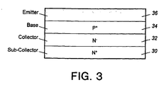
- the layers are grown in series on top of each other as shown in Fig. 3.
- the first layer 30 is an N + InGaAs sub-collector layer which contains a large concentration of silicon atoms.
- a collector region 32 is formed on top of the sub-collector as an N - GaAs layer with a lower concentration of silicon.
- a P + base layer 34 is formed thereon of GaAs with beryllium doping.
- An emitter layer 36 is then formed on top of the base layer.
- the crystal structure 10 of a sub-collector of a prior art device is shown in Fig. 1.
- gallium atoms may reside in the crystal structure at interstitial locations. Since these atoms are not tightly bonded to the crystal structure, they often diffuse through the structure, especially during the growth of the other layers. Since the growth is relatively slow, on the order of one layer of atoms per second, the interstitial gallium can diffuse as the device is grown. Problems arise when the interstitial gallium reaches the base layer. In that layer, the interstitial gallium atoms from the sub-collector tends to displace the beryllium atoms from their positions in the base so that they are free to diffuse to the emitter. The result is poor reliability of the device.
- one object of the invention is to provide a novel HBT device having phosphorus doping in the sub-collector.
- a further object of this invention is to improve the reliability of HBT devices by preventing the diffusion of beryllium atoms from the base to the emitter.
- the bond between the gallium and phosphorus atoms is the strongest bond among the bonds in InAs, GaAs, InP or GaP. Therefore, it is the most stable bond.
- By bonding the interstitial gallium it moved to a lattice site and thus is no longer free to diffuse. Since it does not diffuse, the chance of beryllium diffusing out of the base layer decreases, thus preventing the reliability problems previously noted.
- the interstitial gallium concentration can be reduced by doping with phosphorus at a level of 1 x 10 18 to 1 x 10 19 atoms per cubic centimeter. At this concentration of phosphorus, movement of interstitial gallium and beryllium diffusion is prevented.
- the doping can also be in the collector layer.
- Another way of preventing the diffusion of interstitial gallium in these devices is to provide a collector of InP. Having the phosphorus in such a layer then removes the interstitial gallium as it diffuses from the sub-collector. Thus, it is prevented from reaching the base so that the same end result is achieved.
- the InP has a higher breakdown voltage than a layer of InGaAs.
- the sub-collector region could also be replaced with a layer of InP so that gallium is not present at all thus preventing the problem in this manner as well.
Landscapes
- Bipolar Transistors (AREA)
Abstract
Description
Claims (13)
- A heterojunction bipolar transistor, comprising:a sub-collector containing at least one group-III material;a collector provided on said sub-collector;a base provided on said collector;an emitter provided on said base; anda group-V material included in one of said sub-collector and collector which bonds to any interstitial group-III atoms and moves them to a lattice site.
- The transistor according to claim 1, wherein the group-III material is selected from the group consisting of gallium and indium.
- The transistor according to claim 1, wherein the group-V material is phosphorus.
- The transistor according to claim 3, wherein the phosphorus is included in the sub-collector.
- A transistor according to claim 3, wherein the phosphorus is included in the collector.
- The transistor according to claim 1, wherein the group-V material is included by doping.
- The transistor according to claim 6, wherein the concentration of dopant is 1 X 10¹⁸ to 1 x 10¹⁹ atoms per cubic centimeter.
- The transistor according to claim 6, wherein the dopant is phosphorus.
- An InP based heterojunction bipolar transistor comprising:wherein phosphorus dopant is included in said sub-collector layer so as to bond with any interstitial gallium and move it to a lattice site.an N+ sub-collector layer of InGaAs with a high concentration of Si;an N- collector layer provided on said sub-collector containing InGaAs with a low concentration of Si;a P+ base layer provided on said collector containing InGaAs and a large concentration of Be; andan emitter layer provided on said base;
- A method of forming a heterojunction bipolar transistor, comprising the steps of:forming a sub-collector containing at least one group-III material;forming a collector on said sub-collector;forming a base on said collector;forming an emitter on said base; andincluding a group-V material in one of said sub-collector and said collector for removing interstitial group-III atoms.
- The method according to claim 10, comprising selecting the group-III material from the group consisting of gallium and indium.
- The method according to claim 10, comprising utilizing phosphorus as the group-V material.
- The method according to claim 12, wherein the phosphorus is included by doping.
Applications Claiming Priority (2)
| Application Number | Priority Date | Filing Date | Title |
|---|---|---|---|
| US09/667,910 US6680497B1 (en) | 2000-09-22 | 2000-09-22 | Interstitial diffusion barrier |
| US667910 | 2000-09-22 |
Publications (2)
| Publication Number | Publication Date |
|---|---|
| EP1191599A2 true EP1191599A2 (en) | 2002-03-27 |
| EP1191599A3 EP1191599A3 (en) | 2004-12-15 |
Family
ID=24680167
Family Applications (1)
| Application Number | Title | Priority Date | Filing Date |
|---|---|---|---|
| EP01119652A Withdrawn EP1191599A3 (en) | 2000-09-22 | 2001-08-21 | Interstitial diffusion barrier |
Country Status (4)
| Country | Link |
|---|---|
| US (1) | US6680497B1 (en) |
| EP (1) | EP1191599A3 (en) |
| JP (1) | JP3958005B2 (en) |
| TW (1) | TW508831B (en) |
Families Citing this family (1)
| Publication number | Priority date | Publication date | Assignee | Title |
|---|---|---|---|---|
| JP4727903B2 (en) * | 2001-01-03 | 2011-07-20 | ウルトラシェイプ リミティド | Non-invasive ultrasound body contouring |
Family Cites Families (8)
| Publication number | Priority date | Publication date | Assignee | Title |
|---|---|---|---|---|
| JPS60200900A (en) * | 1984-03-26 | 1985-10-11 | Sumitomo Electric Ind Ltd | Semiconductor single crystal of group iii-v compound having low dislocation density |
| FR2625613B1 (en) * | 1987-12-30 | 1990-05-04 | Labo Electronique Physique | |
| US5139960A (en) * | 1988-11-28 | 1992-08-18 | Xerox Corporation | Interstitital doping in III-V semiconductors to avoid or suppress DX center formation |
| US5231298A (en) * | 1991-01-24 | 1993-07-27 | Spire Corporation | GaAs device having a strain-free c-doped layer |
| EP0717435A1 (en) * | 1994-12-01 | 1996-06-19 | AT&T Corp. | Process for controlling dopant diffusion in a semiconductor layer and semiconductor layer formed thereby |
| JP3310514B2 (en) * | 1995-12-22 | 2002-08-05 | シャープ株式会社 | Semiconductor device |
| US6107151A (en) * | 1997-05-09 | 2000-08-22 | Research Triangle Institute | Heterojunction bipolar transistor and method of manufacturing |
| US6049099A (en) * | 1998-05-11 | 2000-04-11 | The United States Of America As Represented By The Secretary Of The Air Force | Cadmium sulfide layers for indium phosphide-based heterojunction bipolar transistors |
-
2000
- 2000-09-22 US US09/667,910 patent/US6680497B1/en not_active Expired - Lifetime
-
2001
- 2001-08-21 EP EP01119652A patent/EP1191599A3/en not_active Withdrawn
- 2001-09-07 JP JP2001271266A patent/JP3958005B2/en not_active Expired - Fee Related
- 2001-09-19 TW TW090123093A patent/TW508831B/en not_active IP Right Cessation
Also Published As
| Publication number | Publication date |
|---|---|
| JP3958005B2 (en) | 2007-08-15 |
| JP2002151521A (en) | 2002-05-24 |
| TW508831B (en) | 2002-11-01 |
| US6680497B1 (en) | 2004-01-20 |
| EP1191599A3 (en) | 2004-12-15 |
Similar Documents
| Publication | Publication Date | Title |
|---|---|---|
| US5656514A (en) | Method for making heterojunction bipolar transistor with self-aligned retrograde emitter profile | |
| US5298763A (en) | Intrinsically doped semiconductor structure and method for making | |
| KR100725689B1 (en) | Heterobipolar transistors | |
| KR100289473B1 (en) | Multi-layer Base Heterojunction Device and Manufacturing Method Thereof | |
| EP0504875A2 (en) | Bipolar transistor and method of fabricating the same | |
| US5302841A (en) | Heterojunction bipolar transistor | |
| SE9603738D0 (en) | A method for producing a bipolar semiconductor device and a bipolar semiconductor device | |
| US6271061B1 (en) | Fabrication of insulated gate bipolar devices | |
| US6171920B1 (en) | Method of forming heterojunction bipolar transistor having wide bandgap, low interdiffusion base-emitter junction | |
| US6680497B1 (en) | Interstitial diffusion barrier | |
| JP3157098B2 (en) | Resonant tunneling hot electron transistor | |
| US6967144B1 (en) | Low doped base spacer for reduction of emitter-base capacitance in bipolar transistors with selectively grown epitaxial base | |
| JP2770583B2 (en) | Method of manufacturing collector-top heterojunction bipolar transistor | |
| KR100754561B1 (en) | Silicon germanium transistor with improved cutoff frequency | |
| JP2600969B2 (en) | Germanium-gallium arsenide junction and heterostructure bipolar transistor | |
| JP4239333B2 (en) | Heterojunction bipolar transistor | |
| EP0607935A2 (en) | Heterojunction bipolar transistor fabrication method with low temperature base growth | |
| GB2175443A (en) | Bipolar semiconductor device | |
| JPH04196327A (en) | Bipolar transistor and manufacture thereof | |
| JPH02183571A (en) | Varactor diode | |
| JPH0397230A (en) | Manufacture of semiconductor device | |
| JPH02262339A (en) | Semiconductor device | |
| JPH02148846A (en) | bipolar transistor | |
| JPH02299241A (en) | P-n-p-type bipolar transistor | |
| JPS6376372A (en) | Semiconductor device |
Legal Events
| Date | Code | Title | Description |
|---|---|---|---|
| PUAI | Public reference made under article 153(3) epc to a published international application that has entered the european phase |
Free format text: ORIGINAL CODE: 0009012 |
|
| AK | Designated contracting states |
Kind code of ref document: A2 Designated state(s): AT BE CH CY DE DK ES FI FR GB GR IE IT LI LU MC NL PT SE TR |
|
| AX | Request for extension of the european patent |
Free format text: AL;LT;LV;MK;RO;SI |
|
| RAP1 | Party data changed (applicant data changed or rights of an application transferred) |
Owner name: NORTHROP GRUMMAN CORPORATION |
|
| RAP1 | Party data changed (applicant data changed or rights of an application transferred) |
Owner name: NORTHROP GRUMMAN CORPORATION |
|
| PUAL | Search report despatched |
Free format text: ORIGINAL CODE: 0009013 |
|
| AK | Designated contracting states |
Kind code of ref document: A3 Designated state(s): AT BE CH CY DE DK ES FI FR GB GR IE IT LI LU MC NL PT SE TR |
|
| AX | Request for extension of the european patent |
Extension state: AL LT LV MK RO SI |
|
| STAA | Information on the status of an ep patent application or granted ep patent |
Free format text: STATUS: THE APPLICATION HAS BEEN WITHDRAWN |
|
| 17P | Request for examination filed |
Effective date: 20050117 |
|
| 18W | Application withdrawn |
Effective date: 20050211 |