Technical Field
-
The present invention relates mainly to ceramic substrates
used as a device for producing or examining semiconductors, such
as ceramic substrates for hot plates (ceramic heaters),
electrostatic chucks and wafer probers.
Background Art
-
As the device for producing or examining semiconductors
including an etching device, a chemical vapor deposition device
and the like, heaters or wafer probers and the like using
substrates made of metal such as stainless steel or aluminum
alloy, have been conventionally used.
-
However, heaters made of metal have problems that they
have poor temperature control characteristics and they are heavy
and bulky since they are thick; and also have another problem
that they have poor corrosion resistance to corrosive gases.
-
In order to solve such problems, heaters which use ceramic
such as aluminum nitride have been developed in place of heaters
made of metal.
-
Since such ceramic heaters have the advantage that a warp
and the like of ceramic substrates can be prevented even if they
are not made so thick due to high rigidity thereof, they are
especially suitable for wafer probers or electrostatic chucks.
-
In recent years, as the semiconductor wafer becomes larger
and the diameter thereof becomes larger, the diameter of ceramic
substrates used in electrostatic chucks and the like used for
producing or examining of semiconductor wafers are required to
be bigger so as to put the enlarged semiconductor wafers thereon.
Thus, for example, a hot plate having a diameter of 300mm and
a thickness of 17mm composed of aluminum nitride ceramic is
disclosed in JP Kokai Hei 11-74064 and so on.
Summary of the Invention
-
There existed a problem that such enlargement of an
electrostatic chuck and the like results in the deterioration
of a temperature-risingpropertyoraheatuniformityofaceramic
substrate, those are the properties being demanded at the
production of semiconductor devices and the like.
-
The inventors of the present invention studied earnestly
to solve the above problems. Consequently, they have found that
the reason why the temperature-rising property or the heat
uniformity of such a large ceramic substrate having a diameter
exceeding 250mm is deteriorated is the increase of a heat capacity
of a ceramic substrate. Simultaneously, they have found that
the temperature-rising property and the heat uniformity can be
improved: by lowering a barrier of heat conduction between
ceramic particles through the improvement of sinterability by
incorporating oxygen in a ceramic substrate ; and by the reduction
of the heat capacity itself through the adjustment of the
thickness of the ceramic substrate to 25 mm or less.
-
Moreover, in the case of a large ceramic substrate which
has a diameter exceeding 250 mm, if the thickness thereof is
adjusted to 25 mm or less, a warp tends to be generated at a
high temperature. They have found that the warp can be prevented
almost completely by: forming a conductor at the position of
60% in a thickness-direction from the bottom face opposite to
a wafer treating face of the ceramic substrate ; and using a nitride
ceramic containing oxygen or an oxide ceramic as the ceramic.
Thus, they have accomplished the present invention.
-
In case a disk-shaped ceramic substrate has a diameter
of 250 mm or more, the ceramic substrate is adjusted to have
a thickness of 25 mm or less in order to reduce the heat capacity
of the ceramic substrate. In such a case, if a resistance heating
element is disposed inside the ceramic substrate, the distance
between the resistance heating element and the heating face
becomes shorter correspondingly, resulting in an occurrence of
a temperature distribution similar to the pattern of the
resistance heating element. The present invention has been
accomplished through the finding that disposing of a conductor,
such as a resistance heating element, on the back side of a ceramic
substrate makes it possible to keep the substantial distance
between the heating face and the resistance heating element,
and can improve the temperature-rising property and the heat
uniformity.
-
Besides, although the adjustment of the thickness of a
ceramic substrate to 25 mm or less makes the ceramic substrate
apt to warp at a high temperature, the present invention can
also prevent such a warp.
-
In JP Kokai Hei 11-74064, a hot plate composed of aluminum
nitride ceramic having a diameter of 300 mm and a thickness of
17 mm is disclosed, but there is no description or suggestion
on the problem on the warp at a high temperature. The publication,
therefore, never affect the novelty or inventive step of the
present invention.
-
A first aspect of the present invention is a ceramic
substrate for a semiconductor-producing/examining device
having a conductor formed on a surface of the ceramic substrate
or inside the ceramic substrate, wherein said substrate is
containing oxygen and has a disc form,
the diameter thereof exceeding 250 mm and a thickness
thereof being 25 mm or less.
-
A second aspect of the present invention is a ceramic
substrate for a semiconductor-producing/examining device
having a conductor formed on a surface of the ceramic substrate,
wherein said substrate has a disc form,
the diameter thereof exceeding 250 mm and a thickness
thereof being 25 mm or less.
-
The above-mentioned first and second aspects of inventions
are different in the position where a conductor is formed and
in the respect whether oxygen is contained or not, but they are
the same with respect to the other constituent features. The
contents of the two inventions, therefore, will be described
together below.
Brief Description of Drawings
-
- Fig. 1 is a longitudinal sectional view schematically
showing an electrostatic chuck that is an embodiment of a ceramic
substrate for use in a device for producing or examining a
semiconductor according to the present invention.
- Fig. 2 is an A-A line sectional view of the electrostatic
chuck shown in Fig. 1.
- Fig. 3 is a B-B line sectional view of the electrostatic
chuck shown in Fig. 1.
- Fig. 4 is a sectional view schematically showing an example
of an electrostatic electrode of an electrostatic chuck.
- Fig. 5 is a sectional view schematically showing an example
of an electrostatic electrode of an electrostatic chuck.
- Fig. 6 is a sectional view schematically showing a wafer
prober that is an embodiment of a ceramic substrate of the present
invention.
- Fig. 7 is an A-A line sectional view in the wafer prober
shown in Fig. 6.
- In Fig. 8, (a) to (d) are sectional views schematically
showing a part of the manufacture process of an electrostatic
chuck.
- Fig. 9 is a sectional view schematically showing a hot
plate that is an embodiment of a ceramic substrate of the present
invention.
-
Explanation of symbols
-
- 101
- Electrostatic chuck
- 1, 43
- Ceramic substrate
- 2, 22, 32a, 32b
- Chuck positive electrostatic layer
- 3, 23, 33a, 33b
- Chuck negative electrostatic layer
- 2a, 3a
- Semicircle arc part
- 2b, 3b
- Comb teeth-shaped part
- 4
- Ceramic dielectric film
- 5, 49
- Resistance heating element
- 6, 18
- External terminal pin
- 9
- Silicon wafer
- 11
- Bottomed hole
- 12
- Through hole
- 16
- Conductor-filled through hole
- 42
- Chuck top conductor layer
- 45
- Guard electrode
- 46
- Ground electrode
- 47
- Groove
- 48
- Suction hole
Detailed Description of the Invention
-
The ceramic substrate for a semiconductor
producing/examining device according to the present invention
is a ceramic substrate having a conductor formed on a surface
of the ceramic substrate or inside the ceramic substrate, wherein
said substrate is containing oxygen and has a disc form,
the diameter thereof exceeding 250 mm and a thickness thereof
being 25 mm or less. It is desirable that the above-mentioned
ceramic substrate contains oxygen or is an oxide ceramic.
-
In the ceramic substrate of the present invention, the
above-mentioned ceramic substrate is made large to have a
diameter thereof exceeding 250 mm, and at the same time, the
thickness thereof being 25mm or less, so that the increase in
the weight of the whole ceramic substrate is suppressed. Thus,
the heat capacity of the ceramic substrate can be prevented from
becoming too large, resulting in a ceramic substrate having
uniform enough temperature distribution that raises no problems
in the processing of semiconductor wafers and the like.
-
If the thickness of a ceramic substrate exceeds 25 mm,
the heat capacity of the ceramic substrate becomes large.
Particularly, if the ceramic substrate is heated and cooled by
using temperature control means, the large heat capacity causes
the deterioration in temperature-following property.
-
The thickness of the ceramic substrate is desirably 10
mm or less, and more desirably 5 mm or less. If it exceeds 10
mm, the heat capacity of the ceramic substrate at a temperature
of 200 °C or more will become large, and the temperature
controllability thereof, and the temperature uniformity of the
face on which a semiconductor wafer will be placed, tend to become
poor.
-
The above-mentioned ceramic substrate is used in a
temperature range of 100 to 700 °C. This is because in a
temperature range of 100 °C or more, the Young's modulus of the
ceramic is lowered and the ceramic tends to warp, so the
advantageous effect of the present invention is beneficial.
-
The above-mentioned ceramic substrate desirably has a
plurality of through holes in which lifter pins for a
semiconductor wafer will be inserted. The reason is that when
a ceramic substrate has through holes, the Young's modulus is
lowered at a temperature of 100 °C or more, resulting in the
release of the stress generated during processing, thus the
substrate tends to warp. The advantageous effect of the present
invention, therefore, become significant. The diameter of the
through holes is desirably 0.5 mm to 30 mm.
-
In the ceramic substrate of the present invention, a
silicon wafer is put on a surface of the ceramic substrate in
the state that they contact each other. Besides, the silicon
wafer may be supported by lifter pins and the like and held in
the state that a given interval is kept between the silicon wafer
and the ceramic substrate (reference to Fig. 9). Such a face
on which a semiconductor wafer is placed or held will, in the
following description, be expressed as a wafer treating face.
When a semiconductor wafer is supported with a supporting pin,
for example, a concave portion is formed in a ceramic substrate
and a supporting pin is fitted in a concave portion so that its
tip slightly projects from the wafer treating face and a
semiconductor wafer is supported by the supporting pin.
-
When heating is conducted while a distance between a
ceramic substrate and a semiconductor wafer is kept constant,
the distance is desirably 50 to 5000 µm.
-
In the case that heating is conducted while a distance
between a ceramic substrate and a semiconductor wafer is kept
constant, unless the distance between the semiconductor wafer
and the holding face of the ceramic substrate is made to be constant,
the semiconductor wafer cannot be heated uniformly. For this
reason, there is a necessity of minimizing the warp amount of
a ceramic substrate thus, the present invention can act
particularly advantageously.
-
In the present invention, the warp amount is desirably
less than 70 µm in a temperature range of 100 to 700 °C. This
is because if it exceeds 70 µm, a distance between a treating
face (the heating face) of a ceramic substrate and a semiconductor
wafer becomes uneven and the semiconductor wafer cannot be heated
uniformly.
-
The reason why the diameter of the ceramic substrate is
set to be larger than 250 mm is that a diameter of a semiconductor
wafer is becoming mainly 10 inches or more, and there is also
a need for the ceramic substrates to become larger. Thus, the
above-mentioned ceramic substrate is preferably 12 inches (300
mm) or more. This is because such a ceramic substrate will become
the main stream of semiconductor wafers of the next generation.
In addition, ceramic substrates having a diameter larger than
250 mm tend to warp due to their own weight and the like at a
high temperature. Such a warp remarkably occurs in a ceramic
with a thickness of 25 mm or less. In the present invention,
by providing a conductor in a specific region of a ceramic wherein
the warp easily occurs at such a high temperature, such a warp
can be prevented.
-
The above-mentioned conductor is desirably disposed: in
a region up to the position of 60% in the thickness-direction
from the face opposite to the wafer treating face of the ceramic
substrate; or on the above-mentioned face opposite to the wafer
treating face. The warp is caused by the own weight or, in the
case of ceramic substrates for wafer probers (hereinafter,
mentioned as wafer probers), is caused by the pressure of probing.
Therefore, when a ceramic substrate warps, a pulling force is
applied on the face opposite to the wafer treating face. In
the present invention, a ceramic substrate becomes able to resist
to such a pulling force by providing it with a conductor and,
thus the warp can be prevented.
-
Examples of the above-mentioned conductor include a
conductive ceramic, a metal foil, a metal sintered body, a metal
wire and the like . Generally, even at a high temperature, a Young's
modulus of a metal does not drop easily. Hence, even if the
Young's modulus of a ceramic drops at a high temperature, the
presence of a metal foil, metal sintered body, metal wire and
the like can prevent the drop in a Young's modulus of the whole.
Moreover, since the above-mentioned conductive ceramic also has
a bonding structure or a crystal structure similar to those of
metal due to the fact that the conductive ceramic is conductive,
its Young's modulus is not easily lowered at a high temperature
and a ceramic substrate, therefore, can be prevented from warping
at a high temperature.
-
Also, in the case in which the above-mentioned conductor
serves as a resistance heating element, it is desirably disposed:
in a region up to the position of 50% in the thickness-direction
from the face opposite to the wafer treating face of the ceramic
substrate; or on the above-mentioned face opposite to the wafer
treating face of the ceramic substrate. This is because: when
heat is transmitted from a heating element to a wafer treating
face through the inside of a ceramic substrate, the heat diffuses
in the ceramic substrate to produce uniform heat, thus as a
distance between the wafer treating face and the heating element
becomes larger, the surface temperature of the wafer treating
face tends to be uniform.
-
In the ceramic substrate for use in a semiconductor device
according to the present invention, a ceramic substrate having
a Young's modulus of 280 GPa or more in a temperature range of
25 to 800 °C is desirably employed.
-
This is because if a Young's modulus is less than 280 GPa,
the rigidity is too low and, therefore, it is difficult to reduce
the warp amount during the heating and then, the warp may cause
the damage of a semiconductor wafer.
-
In the present invention, it is desirable that there are
no pores, or even if there are pores, the pore diameter of the
largest pore is 50 µm or less.
-
When there are no pores, a breakdown voltage at a high
temperature becomes particularly high. On the other hand, when
there are pores, a fracture toughness value becomes high.
Accordingly, which design to take depends upon the required
characteristics.
-
The reason why a high fracture toughness value is caused
by the presence of pores is not clear, but it is presumed that
the development of cracks is stopped by the pores.
-
In the present invention, the largest pore desirably has
a pore diameter of 50 µm or'less because if it exceeds 50 µm,
a high breakdown voltage characteristic cannot be kept
particularly at a temperature of 200 °C or more.
-
The pore diameter of the largest pore is more desirably
10 µm or less because a warp amount decreases at a temperature
of 200 °C or more.
-
The porosity and the pore diameter of the largest pore
are adjusted: by a length of pressing time, pressure and
temperature during sintering; and by an additive such as SiC
or BN. SiC or BN can introduce pores since they inhibit
sintering.
-
At the measurement of the pore diameter of the largest
pore, 5 samples are prepared. Then, after polishing their
surfaces and photographing the surfaces of the samples at 10
points for every samples with an electron microscope at a
magnification of 2000 to 5000 times, the largest pore diameter
is chosen in every photograph taken and the average of the 50
shots is defined as the largest pore diameter.
-
The above-mentioned nitride ceramic substrate desirably
contains 0.05 to 10% by weight of oxygen. This is because, when
the oxygen content is less than 0.05% by weight, a high breakdown
voltage cannot be kept and a warp at a high temperature cannot
be prevented, and, on the other hand, when the content exceeds
10% by weight, a breakdown voltage drops due to the drop of the
high breakdown voltage characteristic of the oxide at a high
temperature. This is also because, when the oxygen amount thereof
exceeds 10% by weight, temperature rising/falling property
becomes poor due to the drop in heat conductivity. Particularly,
a content of 0.1 to 5% by weight is optimum.
-
Oxygen can be introduced: by heating raw material in the
air or in oxygen; or by adding a sintering aid.
-
A ceramic containing oxygen (a nitride ceramic containing
oxygen, a carbide ceramic containing oxygen and an oxide ceramic)
do not easily warp at a high temperature because their Young's
modulus do not easily drop at a high temperature.
-
The porosity is measured by an Archimedes' method. A
sintered body is pulverized, and then the pulverized pieces are
put in an organic solvent or mercury to determine its volume.
-
Then the true specific gravity of the pieces is obtained
from the weight and the measured volume thereof, and the porosity
is calculated from the true specific gravity and apparent
specific gravity.
-
The ceramic material constituting the ceramic substrate
of the present invention is not particularly limited and is
exemplified by a nitride ceramic, a carbide ceramic and an oxide
ceramic and the like.
-
Examples of the above-mentioned nitride ceramic include
a metal nitride ceramic such as aluminum nitride, silicon nitride,
boron nitride and titanium nitride and the like.
-
Examples of the above-mentioned carbide ceramic include
a metal carbide ceramic such as silicon carbide, zirconium
carbide, titanium carbide, tantalum carbide and tungsten carbide
and the like.
-
Examples of the above-mentioned oxide ceramic include a
metal oxide ceramic such as alumina, zirconia, cordierite and
mullite and the like.
-
These ceramics may be used either alone or in combination
of two or more kinds of them.
-
Among these ceramics, a nitride ceramic and an oxide
ceramic are preferable because they do not easily cause a warp
at a high temperature.
-
Among a nitride ceramic, aluminum nitride is most desirable
because it has the highest heat conductivity as high as 180 W/m·
K.
-
In the present invention, the ceramic substrate desirably
contains a sintering aid.
-
As the sintering aid, an alkali metal oxide, an alkaline
earth metal oxide and a rare-earth oxide can be used. Among
these sintering aids, CaO, Y2O3, Na2O, Li2O and Rb2O3 are desirable
particularly. Alumina may also be used. The content thereof
is desirably 0.1 to 20% by weight.
-
In the present invention, the ceramic substrate desirably
contains 50 to 5000 ppm of carbon.
-
This is because, by incorporating carbon into the substrate,
the ceramic substrate is made to be black, thus sufficient use
of radiation heat is possible in the case of using the ceramic
substrate as a heater.
-
The carbon may be either amorphous one or crystalline one.
This is because the use of amorphous carbon can prevent a drop
in a volume resistivity at a high temperature and the
use of crystalline carbon can prevent a drop in a heat conductivity
at a high temperature. Accordingly, depending on the purpose,
both crystalline carbon and amorphous carbon may be used together.
The content of, carbon is desirably 200 to 2000 ppm.
-
When the ceramic substrate contains carbon, the ceramic
substrate desirably contains carbon so as to have a brightness
of N6 or less based on the provision given in JIS Z 8721. This
is because a ceramic substrate having such a brightness is
superior in radiant heat capacity and covering-up property.
-
Herein, the brightness N is defined as follows: the
brightness of ideal black is made to 0; that of ideal white is
made to 10; respective colors are divided into 10 parts in the
manner that the brightness of the respective colors is recognized
stepwise between the brightness of black and that of white at
equal intensity intervals; and the resultant parts are indicated
by symbols N0 to N10, respectively.
-
Actual brightness is measured by comparison with color
chips corresponding to N0 to N10. One place of decimals in this
case is made to 0 or 5.
-
The ceramic substate of the present invention is a ceramic
substrate used for a device for producing semiconductors or
examining semiconductors. Examples of the concrete device
include an electrostatic chuck, a wafer prober, a hot plate and
a susceptor and the like.
-
Fig. 1 is a longitudinal sectional view schematically
showing an example of an electrostatic chuck, which is an
embodiment of a ceramic substrate of the present invention. Fig.
2 is a sectional view taken along the A-A line in the electrostatic
chuck illustrated in Fig. 1. Fig. 3 is a sectional view taken
along the B-B line in the electrostatic chuck illustrated in
Fig. 1.
-
In this electrostatic chuck 101, an electrostatic
electrode layer comprising a chuck positive electrostatic layer
2 and a chuck negative electrostatic layer 3 is embedded in a
ceramic substrate 1 in a circular shape as viewed from the above.
A silicon wafer 9 is placed on the electrostatic chuck 101, which
is grounded.
-
Since a ceramic layer which is formed on this electrostatic
electrode layer so as to cover the electrostatic electrode layer,
functions as a dielectric film for adsorbing a silicon wafer,
it will be referred to a ceramic dielectric film 4, hereinafter.
-
As illustrated in Fig. 2, the chuck positive electrostatic
layer 2 comprises a semicircular arc part 2a and a comb
teeth-shaped part 2b and the chuck negative electrostatic layer
3 similarly comprises a semicircular arc part 3a and a comb
teeth-shaped part 3b. These chuck positive electrostatic layer
2 and chuck negative electrostatic layer 3 are arranged opposite
to each other so that the comb-teeth-shaped parts 2b and 3b cross
each other. The + side and the - side of a direct power source
are connected to the chuck positive electrostatic layer 2 and
chuck negative electrostatic layer 3, respectively. Thus, a
direct current V2 is applied thereto.
-
In order to control the temperature of a silicon wafer
9, resistance heating elements 5 in a concentric configuration
as viewed from the above are disposed inside the ceramic substrate
1, and external terminal pins 6 are connected and fixed to both
ends of each of the resistance heating elements 5 so that a voltage
V1 can be applied. Although not shown in Figs. 1,2, in the ceramic
substrate 1, bottomed holes 11 in which temperature measuring
devices are inserted; and through holes 12 through which lifter
pins (not shown) for supporting and moving up and down a silicon
wafer 9 are inserted, are formed. The resistance heating
elements 5 may also be disposed on the bottom face of the ceramic
substrate. The ceramic substrate 1 may have an RF electrode
embedded therein based on the necessity.
-
When the electrostatic chuck 101 is caused to function,
a direct voltage V2 is applied between the chuck positive
electrostatic layer 2 and the chuck negative electrostatic layer
3. Thus, a silicon wafer 9 is adsorbed to be fixed to these
electrodes through a ceramic dielectric film 4 by the
electrostatic action of the chuck positive electrostatic layer
2 and the chuck negative electrostatic layer 3. After fixing
the silicon wafer 9 to an electrostatic chuck 101 in this manner,
the silicon wafer 9 is subjected to various treatments such as
CVD and the like.
-
The above electrostatic chuck is equipped with
electrostatic electrode layers and resistance heating elements
and has a structure, for example, shown in Figs. 1 to 3.
Hereinafter, among the parts constituting the above-mentioned
electrostatic chuck, parts which have not been described in the
description on the above-mentioned ceramic substrate will be
explained.
-
A ceramic dielectric film 4 on the electrostatic electrodes
is desirably made of the same material as the other parts of
the ceramic substrate because a green sheet and the like can
be manufactured in the same process and a ceramic substrate can
bemanufacturedvia a single sintering operation after laminating
those sheets.
-
It is desirable that the above-mentioned ceramic
dielectric film, like the other portions of the ceramic substrate,
contains carbon since an electrostatic electrode can be hidden
and radiation heat can be utilized.
-
The above-mentioned ceramic dielectric film desirably
contains an alkali metal oxide, an alkaline earth metal oxide
or a rare-earth oxide because these serve as a sintering aid
and the like, resulting in formation of a high-density dielectric
film.
-
The thickness of the above-mentioned ceramic dielectric
film is desirably 50 to 5000 µm. This is because of the following
reasons: if the ceramic dielectric film has a thickness less
than 50 µm, the film is too thin to obtain a sufficient breakdown
voltage and the ceramic dielectric film may have a dielectric
breakdown when a silicon wafer is placed and adsorbed; and if
the thickness of the above-mentioned ceramic dielectric film
exceeds 5000 µm, a long distance between a silicon wafer and
an electrostatic electrode lowers the ability of adsorbing the
silicon wafer. The thickness of the ceramic dielectric film
is more desirably 100 to 1500 µm.
-
Examples of the electrostatic electrode formed inside the
ceramic substrate include sintered bodies of metal or conductive
ceramic and metal foils. Desirable metal sintered body is those
made of at least one selected from tungsten and molybdenum. The
metal foils are also desirable to be made of the same material
as the metal sintered body. This is because these metals are
hard to be oxidized and have sufficient conductivities as an
electrode. As a conductive ceramic, at least one selected from
carbides of: tungsten; and molybdenum can be employed.
-
Figs. 4,5 are horizontal sectional views schematically
illustrating electrostatic electrodes in other electrostatic
chucks. In the electrostatic chuck 20 shown in Fig. 4, a chuck
positive electrostatic layer 22 and a chuck negative
electrostatic layer 23, both being in a semicircular shape, are
formed inside the ceramic substrate 1. In the electrostatic
chuck illustrated in Fig. 5, are arranged chuck positive
electrostatic layers 32a, 32b and chuck negative electrostatic
layers 33a, 33b, both types of layers having a shape obtained
by dividing a circular shape in four. Two positive electrostatic
layers 22a, 22b and two negative electrostatic layers 33a and
33b are formed so as to cross each other.
-
When forming electrodes in a shape obtained by dividing
an electrode having a circular shape and the like, the number
of divided pieces is not particularly limited and may be 5 or
more. The shape of the electrode is also not limited to a sector
form.
-
A resistance heating element may be formed inside a ceramic
substrate as illustrated in Fig. 1, and may also be disposed
on the bottom face of the ceramic substrate. When a resistance
heating element is disposed, a supporting case into which an
electrostatic chuck is fitted may be provided with an inlet for
blowing a coolant, such as the air, as cooling means.
-
Examples of resistance heating elements include sintered
body made of metal or conductive ceramic, metal foils and metal
wires and the like. As the metal sintered body, at least one
selected from tungsten and molybdenum is desirable because these
metals are relatively hard to be oxidized and have resistivities
sufficient to generate heat.
-
As the conductive ceramic, at least one selected from
carbides of: tungsten; and molybdenum can be employed.
-
Furthermore, when a resistance heating element is formed
on the bottom face of a ceramic substrate, it is desirable to
use noble metal (gold, silver, palladium, platinum) or nickel
as the sintered body. Specifically, silver, silver-palladium
and the like can be used.
-
As metal particles to be used for the above-mentioned metal
sintered body, those of a spherical shape, those of a scaly shape,
and mixtures of those of a spherical shape and those of a scaly
shape can be used.
-
A metal oxide may be added in the metal sintered body.
The purpose of using the above-mentioned metal oxide is to let
a ceramic substrate adhere to metal particles firmly. The reason
of the improvement in the adhesion between a ceramic substrate
and metal particles is not clear, but would be as follows: an
oxide film is slightly formed on the surface of the metal particles
and an oxide film is formed on the surface of the ceramic substrate
in the case that the ceramic substrate is made of a non-oxide
ceramic as well as an oxide ceramic. It can be therefore
considered that these oxide films are sintered and integrated
with each other, through the metal oxide, on the surface of the
ceramic substrate so that the metal particles and the ceramic
substrate adhere closely to each other.
-
As the above metal oxide, for example, at least one selected
from lead oxide, zinc oxide, silica, boron oxide (B2O3), alumina,
yttria and titania is desirable because these oxides can improve
the adhesiveness between metal particles and a ceramic substrate
without increasing the resistivity of a resistance heating
element.
-
The amount of the metal oxide is desirably 0.1 part by
weight or more and less than 10 parts by weight per 100 parts
by weight of metal particles because the use of a metal oxide
in this range can improve the adhesiveness between metal
particles and a ceramic substrate without too much increase of
resistivity.
-
The rates of lead oxide, zinc oxide, silica, boron oxide
(B2O3), alumina, yttria and titania, based on 100 parts by weight
of the whole amount of the metal oxides, are preferably 1 to
10 parts by weight for lead oxide, 1 to 30 parts by weight for
silica, 5 to 50 parts by weight for boron oxide, 20 to 70 parts
by weight for zinc oxide, 1 to 10 parts by weight for alumina,
1 to 50 parts by weight for yttria and 1 to 50 parts by weight
for titania. The ratio is preferably adjusted within the scope
that the total amount of these oxides is not over 100 parts by
weight. This is because these ranges are particularly those
where the adhesion to a ceramic substrate can be improved.
-
When a resistance heating element is disposed on the bottom
face of a ceramic substrate, it is desirable that a surface of
the resistance heating element is covered with a metal layer.
The resistance heating element is a sintered body of metal
particles. Hence, if it is exposed, it is oxidized easily and
the oxidization thereof results in a change in the resistivity.
Then, such oxidation can be prevented by covering the surface
with a metal layer.
-
A desirable thickness of the metal layer is 0.1 to 10 µm
because this is the range where the oxidation of a resistance
heating element can be prevented without a change in the
resistivity of the resistance heating element.
-
The metal used for the covering may be any non-oxidizable
metal. Specifically, at least one kind of metal selected from
gold, silver, palladium, platinum and nickel is desirable.
Among them, nickel is more desirable because a resistance heating
element is required to have a terminal for the connection to
a power supply, the terminal being attached to the resistance
heating element through a solder, and nickel can prevent thermal
diffusion of the solder. As a connection terminal, a terminal
pin made of Kovar can be employed.
-
It is to be noted that when a resistance heating element
is formed inside a heater plate, the covering is not required
because the surface of the resistance heating element is never
oxidized. When a resistance heating element is formed inside
a heater plate, a part of the surface of the resistance heating
element may be exposed.
-
A desirable metal foil to be used as a resistance heating
element is those formed as resistance heating elements by pattern
formation through, for example, etching a nickel foil and a
stainless steel foil. The patterned metal foil may also be put
together with a resin film and the like. Examples of the metal
wire include a tungsten wire and a molybdenum wire.
-
When a conductor is formed on the surface and inside the
ceramic substrate of the present invention and the above internal
conductor is at least one of a guard electrode or a ground electrode,
the above-mentioned ceramic substrate functions as a wafer
prober.
-
Fig. 6 is a sectional view schematically showing an
embodiment of the wafer prober of the present invention. Fig.
7 is a sectional view of the wafer prober illustrated in Fig.
6 taken along the A-A line.
-
In this wafer prober 201, grooves 47 in a concentric
configuration as viewed from the above are formed in the surface
of a ceramic substrate 43 in a circular form as viewed from the
above and a plurality of suction holes 48 for sucking a silicon
wafer are provided in apart of the grooves 47. A chuck top
conductor layer 42 for connecting to an electrode of a silicon
wafer is formed, in a circular form, in a greater part of the
ceramic substrate 43 including the grooves 47.
-
On the other hand, on the bottom face of the ceramic
substrate 43, a heating elements 49 in a concentric configuration
as viewed from the above as shown in Fig. 3 are disposed in order
to control the temperature of a silicon wafer. To both ends
of each of the heating elements 49, external terminal pins (not
shown) are connected and fixed.
-
Moreover, a guard electrode 45 and a ground electrode 46
(reference to Fig. 7), both being in a lattice form as viewed
from the above, are arranged inside the ceramic substrate 43
in order to remove a stray capacitor and noise. The materials
of the guard electrodes 45 and ground electrodes 46 may be the
same as those of the electrostatic electrodes.
-
The thickness of the above-mentioned chuck top conductor
layer 42 is desirably 1 to 20 µm because if it is less than 1
µm, the resistivity is too high for the layer to work as an
electrode and, on the other hand, if it exceeds 20 µm, the layer
becomes easier to exfoliate due to the stress that the conductor
has,.
-
As the chuck top conductor layer 42, at least one kind
of metal selected from high-melting point metals such as copper,
titanium, chromium, nickel, noble metals (gold, silver, platinum
and the like), tungsten and molybdenum can be employed.
-
As for a wafer prober having such a structure, a continuity
test can be performed by placing, on the wafer prober, a silicon
wafer having an integrated circuit formed thereon, pressing a
probe card having a tester pin against the silicon wafer and
applying a voltage while heating and cooling.
-
Next, a manufacturing method of the ceramic substrate of
the present invention will be explained with reference to the
sectional views shown in Figs. 8(a) to (d) by taking a
manufacturing method of an electrostatic chuck as an example.
- (1) First, a green sheet 50 is made by preparing a mixed
composition by mixing a powder of ceramic such as oxide ceramic,
nitride ceramic and carbide ceramic with a binder and a solvent
and thereafter shaping the composition. When incorporating
carbon into the composition, the above-mentioned crystalline
carbon or amorphous carbon is used and the amount thereof is
controlled depending upon the desired characteristics.
As the ceramic powder, for example, aluminum nitride,
silicon carbide and the like can be used. A sintering aid such
as yttria may be added based on the necessity.When an amorphous carbon is used as carbon, it is desirable
to produce the amorphous carbon in advance, but it is also possible
that a material that will change to amorphous carbon is mixed
in a green sheet. For example, pure amorphous carbon can be
produced by firing a hydrocarbon made up only of C, H and O,
preferably a saccharide (sucrose or cellulose), in the air at
300 to 500 °C. As a crystalline carbon, pulverized crystalline
carbon black or graphite, which are crystalline, can be employed.Several or one green sheet 50 which will be laminated on
a green sheet on which the electrostatic electrode printed
element 51 has been formed, described later, is a layer that
will become a ceramic dielectric film. The composition thereof,
therefore, may be a composition different from that of the ceramic
substrate, depending upon the purpose and the like.Moreover, it is also possible that a ceramic substrate
is manufactured first, an electrostatic electrode layer is
thereafter formed thereon, and a ceramic dielectric film is
formed further thereon.As a binder, at least one selected from acrylic binders,
ethylcellulose, butyl cellosolve and polyvinyl alcohol is
desirable.Furthermore, as a solvent, at least one selected from
α-terpineol and glycol is desirable.A green sheet 50 is made by shaping the paste obtained
by mixing these materials into a sheet form by a doctor blade
method.To the green sheet 50, a through hole in which a lifter
pin for a silicon wafer will be inserted or a concave portion
in which a thermocouple will be buried may also be formed based
on the necessity. The through hole or the concave portion may
be formed by punching and the like.The thickness of the green sheet 50 is desirably about
0.1 to 5 mm.
- (2) Subsequently, a conductor containing paste that will
become an electrostatic electrode layer or a resistance heating
element is printed to the green sheet 50.
The printing is performed in order that a desired aspect
ratio is obtained, by considering a shrinkage ratio of the green
sheet 50. By this operation, an electrostatic electrode layer
printed element 51 and a resistance heating element layer printed
element 52 are obtained.The printed elements are formed by printing a conductor
containing paste containing a conductive ceramic, metal
particles and the like.As the conductive ceramic particles contained in these
conductor containing pastes, a carbide of tungsten or molybdenum
is the most suitable since they are hard to be oxidized and their
conductivity does not drop easily.As the metal particles, for example, tungsten, molybdenum,
platinum and nickel can be employed.The conductive ceramic particles and the metal particles
desirably have an average particle diameter of 0.1 to 5 µm because
if these particles are too large or too small, it is difficult
to print the conductor containing paste.As such a paste, a conductor containing paste which is
prepared by mixing 85 to 97 parts by weight of metal particles
or conductive ceramic particles, 1.5 to 10 parts by weight of
at least one kind of binder selected from acrylic binders,
ethylcellulose, butyl cellosolve and polyvinyl alcohol and 1.5
to 10 parts by weight of at least one kind of solvent selected
from α-terpineol, glycol, ethylalcohol and butanol is most
suitable.Furthermore, conductor-filled through hole printed
elements 53, 54 are obtained by filling the holes formed by
punching and the like with the conductor containing paste.
- (3) Next, as illustrated in Fig 8(a), a green sheet 50 with
printed elements 51, 52, 53, 54 and a green sheet 50 with no
printed element are laminated. On the green sheet on which an
electrostatic electrode printed element 51 has been formed,
several or one green sheet 50 is laminated. The purpose of
laminating a green sheet 50 having no printed element on the
face where a resistance heating element is formed is to prevent
the trouble that an end surface of a conductor-filled through
hole is exposed and oxidized during the sintering for forming
a resistance heating element. If the sintering for forming a
resistance heating element is performed with the end surface
of the conductor-filled through hole exposed, there is a
necessity of sputtering with metal which are hard to be oxidized,
such as nickel. More desirably, it may also be covered with
an Au-Ni gold solder.
- (4) Next, as illustrated in Fig. 8(b), the green sheet and
the conductor containing paste are sintered by heating and
pressurizing the lamination. The heating temperature is
desirably 1000 to 2000 °C and the pressure is desirably 100 to
200 kg/cm2. The heating and pressurizing are performed in an
inert gas atmosphere. As the inert gas, argon, nitrogen and
the like can be employed. In this step, conductor-filled through
holes 16, 17, a chuck positive electrostatic layer 2, a chuck
negative electrostatic layer 3, a resistance heating element
5 and so on, are formed.
- (5) Next, as illustrated in Fig. 8(c), blind holes 13, 14 for
connecting external terminals are formed.
It is favorable that at least a part of the inner walls
of the blind holes 13, 14 is made conductive and the inner walls
which have been made conductive are connected with a chuck
positive electrostatic layer 2, chuck negative electrostatic
layer 3, resistance heating element 5, and so on.
- (6) Finally, as illustrated in Fig. 8(d), external terminals
6, 18 are attached to the blind holes 13, 14 through a gold solder.
Moreover, based on the necessity, a bottomed hole 12 may be formed,
into which a thermocouple is buried.
-
-
Alloy such as silver-lead, lead-tin and bismuth-tin can
be used as a solder.
-
The thickness of the solder layer is desirably 0.1 to 50
µm because this is the range sufficient to keep a connection
with a solder.
-
An electrostatic chuck 101 (reference to Fig.1) was taken
as an example in the above explanation. When manufacturing a
wafer prober, a ceramic substrate with a resistance heating
element embedded therein can be manufactured first, as in the
case of electrostatic chucks, thereafter a groove in the surface
of the ceramic substrate is formed thereon, and then a metal
layer can be formed by conducting sputtering, plating and the
like to the surface portion where the groove has been formed.
Best Mode for Carrying out the Invention
-
The present invention will be described in more detail
below.
(Examples 1 to 3) Hot plate (reference to Fig. 9)
-
- (1) An aluminum nitride sintered body was obtained by: mixing
100 parts by weight of aluminum nitride powder (manufactured by
Tokuyama Corp., average particle diameter 1.1 µm) which is fired
in the air at 500 °C for one hour, 4 parts by weight of yttrium
oxide (Y2O3: yttria, average particle diameter 0.4 µm) and 11.5
parts by weight of acrylic resin binder; putting the mixture
into a hexagonal columnar mold; and then hot pressing it in a
nitrogen atmosphere under the conditions: at a temperature of
1890 °C and a pressure of 150 kg/cm2 for three hours. Ceramic
substrates having, respectively, a diameter of 280 mm and a
thickness of 19 mm (Example1), a diameter of 310 mm and a thickness
of 5 mm (Example 2) and a diameter of 350 mm and a thickness
of 3mm (Example 3) were obtained by processing the above aluminum
nitride sintered body into disk shapes and varying a surface
grinding amount.
- (2) A conductor containing paste was printed on the bottom
face 91a of the ceramic substrate 91 obtained in the above (1)
by screen printing. The printed pattern was that in a concentric
configuration shown in Fig. 3.
As the conductor containing paste, Solbest PS603D
manufactured by Tokuriki Kagaku Kenkyusho.CO, which has been
used for the formation of plated through holes in printed circuit
boards, was used.This conductor containing paste was a silver-lead paste
and contained 7.5 parts by weight, per 100 parts by weight of
silver, of metal oxides comprising lead oxide (5% by weight),
zinc oxide (55% by weight) , silica (10% by weight) , boron oxide
(25% by weight) and alumina (5% by weight) . The silver powder
had an average particle diameter of 4.5 µm and was in a scaly
shape.
- (3) Next, a resistance heating element 92 was formed by heating
and firing the sintered body printed with the conductor
containing paste at 780 °C, thereby sinter the silver and the
lead in the conductor containing paste and baking them to the
ceramic substrate 91. The silver-lead resistance heating
element 92 had a thickness of 5 µm, a width of 2.4 mm and a volume
resistivity of 7.7 mΩ/□.
- (4) Ametal covering layer 92a (a nickel layer) 1 µm in thickness
was deposited on the surface of the silver-lead heating element
92 by immersing the sintered body prepared in the above (4) in
an electroless nickel plating bath comprising an aqueous solution
containing 80 g/L of nickel sulfate, 24 g/L of sodium
hypophosphite, 12 g/L of sodium acetate, 8 g/L of boric acid
and 6 g/L of ammonium chloride.
- (5) A solder layer was formed by printing a silver-lead solder
paste (manufactured by Tanaka Kikinzoku Kogyo CO.) by screen
printing in a portion to which a terminal for securing the
connection with a power supply will be attached. Subsequently,
by placing a terminal pin 93 made of Kovar on the solder layer
and heating and reflowing at 420 °C, the terminal pin 93 was
attached to a surface of the heating element 92 (the metal covering
layer 92a).
- (6) Then, a ceramic heater 90 (reference to Fig. 9) was obtained
by inserting a thermocouple for temperature control in a bottomed
hole 94, filling with a polyimide resin and curing it at 190
°C for 2 hours.
-
(Test examples 1 to 3)
-
Hot plates were manufactured in the same manner as Example
1 except that they are adjusted to have a diameter of 240 mm
and a thickness of 5 mm (Test example 1) ; a diameter of 310 mm
and a thickness of 30 mm (Test example 2); and a diameter of
300 mm and a thickness of 17 mm without adding any Y2O3 (Test
example 3). In Test example 3, a metal foil serving as a
resistance heating element was embedded in the mold and a formed
position of the heating element was adjusted to the position
33% apart from the back face.
(Test examples 4 to 6)
-
Hot plates were manufactured in the same manner as Example
1 except that they are provided with no heating element and
adjusted to have a diameter of 240 mm and a thickness of 5 mm
(Test example 4); a diameter of 310 mm and a thickness of 30
mm (Test example 5) ; and a diameter of 300 mm and a thickness
of 17 mm (Test example 6).
-
As for the hot plates according to the above-mentioned
Examples 1 to 3 and Test examples 1 to 6, a warp amount at 450
°C, a temperature rise time, temperature uniformity of a surface
and an oxygen amount were examined in the manner described below.
It is to be noted that for the hot plates of Test examples 4
to 6, only the warp amount was examined. The results are shown
in the table.1.
(Examples 4 to 6) Alumina hot plate
-
- (1) Green sheets 50, which were 0.47 mm in thickness, were
obtained: by using a paste containing alumina:93% by weight,
SiO2:5% by weight, CaO:0.5% by weight, MgO:0.5% by weight,
TiO2:0.5% by weight, an acrylic binder:11.5 parts by weight,
a dispersant: 0.5 part by weight and 53 parts by weight of alcohol
comprising 1-butanol and ethanol; and forming it by a doctor
blade method.
- (2) Subsequently, after drying these green sheets at 80 °C
for 5 hours, to the green sheets having a necessity of being
processed, portions which will become through holes, in which
lifter pins for a semiconductor wafer, 1.8 mm, 3.0 mm and 5.0
mm in diameter, respectively, and portions which will become
conductor-filled through holes for being connected with external
terminals were formed by punching.
- (3) Conductor containing paste B was prepared by mixing 100
parts by weight of tungsten particle having an average particle
diameter of 3 µm, 1.9 parts by weight of an acrylic binder, 3.7
parts by weight of α-terpineol solvent and 0.2 part by weight
of a dispersant.
A conductor containing paste layer was formed by printing
this conductor containing paste B to the green sheets 50 by screen
printing. The printed pattern was a pattern in a concentric
configuration.
- (4) Furthermore, conductor containing paste B was filled in
the through hole for conductor-filled through holes for being
connected with external terminals.
On the green sheets 50 with a pattern of a resistance heating
element formed thereon, 34 to 60 sheets of green sheets 50 with
no conductor containing paste printed were stacked on their top
side (the heating face); and the same 13 to 30 green sheets
were stacked on their bottom side. Then, the resultant was
pressed at a temperature of 130 °C and a pressure of 80 kg/cm2
to form a lamination (Fig. 8(a)). The heating element-formed
positions are shown in Table 2.
- (5) Next, alumina plates of 3 mm in thickness were obtained
by degreasing the obtained lamination at 600 °C for 5 hours and
hot pressing them at 1600 °C at a pressure of 150 kg/cm2 for
2 hours. By varying the processing conditions and grinding
conditions , ceramic substrates made of alumina having a diameter
of 280 mm and a thickness of 19 mm (Example 4), a diameter of
310 mm and a thickness of 5 mm (Example 5), and a diameter of
350 mm and a thickness of 3 mm (Example 6), respectively, were
obtained. These ceramic substrates had resistance heating
elements 5 having a thickness of 6 µm and a width of 10 mm therein.
- (6) Subsequently, after the grinding of the plates obtained
in (5) with a diamond grind stone, masks were placed on the bodies,
and bottomed holes (diameter:1.2 mm, depth:2.0 mm) for a
thermocouple were formed on their surfaces by blast treatment
with SiC and the like.
- (7) Furthermore, blind holes 13, 14 were formed by hollowing
out the portions where the conductor-filled through holes were
made (Fig 8(c)), and external terminals 6, 18 made of Kovar were
connected to the blind holes 13, 14 by heating and reflowing
using gold solder comprising Ni-Au (Fig 8(d)) at 700 °C. It
is to be noted that the connection of the external terminals
desirably has a structure wherein a support of tungsten supports
at three points since connection reliability can be secured.
- (8) Next, a plurality of thermocouples for temperature control
were buried in the bottomed holes. Thus, the manufacturing of
the hot plates with resistance heating elements was completed.
-
(Test examples 7 to 9)
-
Ceramic substrates were manufactured in the same manner
as Examples 4 to 6 except that they are adjusted to have a diameter
of 240 mm and a thickness of 5 mm (Test example 7) ; a diameter
of 310 mm and a thickness of 30 mm (Test example 8) ; and a diameter
of 300 mm and a thickness of 17 mm using aluminum nitride without
containing any Y2O3 (Test example 9). The heating element-formed
positions are shown in Table 2.
(Test examples 10 to 12)
-
Hot plates were manufactured in the same manner as Examples
4 to 6 except they are provided with no heating element and adjusted
to a diameter of 240 mm and a thickness of 5 mm (Test example
10) ; a diameter of 310 mm and a thickness of 30 mm (Test example
11); and a diameter of 300 mm and a thickness of 17 mm (Test
example 12).
(Test example 13)
-
A hot plate was manufactured in the same manner as Example
5 except laminating 20 sheets of green sheets 50 on the top side
(heating face) and 19 sheets on the bottom side.
(Test example 14)
-
A hot plate was manufactured in the same manner as Example
5 except laminating 10 sheets of green sheets 50 on the top side
(the heating face) and 29 sheets on the bottom side.
-
As for the hot plates of the above-mentioned Examples 4
to 6 and Test examples 7 to 14, a warp amount at 450°C, a temperature
rise time and temperature uniformity of a surface were examined
in the manner described below. It is to be noted that for the
hot plates of Test examples 10 to 12, only the warp amount was
examined. The results are shown in Table 2.
(Examples 7 to 9) Manufacture of electrostatic chucks made of
AlN with heaters (Figs. 1 to 3)
-
- (1) Next, green sheets 50, which were 0.47 mm in thickness,
were obtained by: using a paste prepared by mixing 100 parts
by weight of aluminum nitride powder (manufactured by Tokuyama
Corp., average particle diameter 1.1 µm) fired in the air at 500
°C for one hour, 1, 2, 4 parts by weight of yttria (average particle
diameter 0.4 µm), 11.5 parts by weight of acrylic binder, 0.5
part by weight of a dispersant and 53 parts by weight of alcohol
comprising 1-butanol and ethanol; and forming it by a doctor
blade method.
- (2) Subsequently, after drying these green sheets 50 at 80
°C for 5 hours, to the green sheets having a necessity of being
processed, portions which will become through holes, in which
lifter pins for a semiconductor, 1.8 mm, 3.0 mm and 5.0 mm in
diameter, respectively, and portions which will become
conductor-filled through holes for being connected with external
terminals were formed by punching.
- (3) Conductor containing paste A was prepared by mixing 100
parts by weight of tungsten carbide particles having an average
particle diameter of 1 µm, 3.0 parts by weight of an acrylic
binder, 3.5 parts by weight of α-terpineol solvent and 0.3 part
by weight of a dispersant.
Conductor containing paste B was prepared by mixing 100
parts by weight of tungsten particles having an average particle
diameter of 3 µm, 1.9 parts by weight of an acrylic binder, 3.7
parts by weight of α-terpineol solvent and 0.2 part by weight
of a dispersant.A conductor containing paste layer was formed by printing
this conductor containing paste A to the green sheets 50.by screen
printing. The printed pattern was a pattern in a concentric
configuration. Moreover, on another green sheet 50, a conductor
containing paste layer having an electrostatic electrode pattern
with a shape shown in Fig. 2 was formed.
- (4) Furthermore, conductor containing paste B was filled in
the through hole for conductor-filled through holes for being
connected with external terminals.
On the green sheets 50 with a pattern of a resistance heating
element formed thereon, 34 to 60 sheets of green sheets 50 with
no conductor containing paste printed were stacked on their top
side (the heating face); and the same 13 to 30 green sheets
were stacked on their bottom side. Then, the resultant was
pressed at a temperature of 130 °C and a pressure of 80 kg/cm2
to form a lamination (Fig. 8(a)). The heating element-formed
positions are shown in Table 2.
- (5) Next, the resulting laminations were processed to
substrates, respectively, having a diameter of 280 mm and a
thickness of 19 mm (Example 7), a diameter of 310 mm and a thickness
of 5 mm (Example 8) and a diameter of 350 mm and a thickness
of 3 mm (Example 9) under nitrogen gas by degreasing the
laminations at 600 °C for 5 hours, hot pressing them at 1890
°C at a pressure of 150 kg/cm2 for 3 hours and varying the processing
conditions and grinding conditions. Thus, plates made of
aluminum nitride were obtained, which had therein resistance
heating elements 5 having a thickness of 6 µm and a width of
10 mm and a chuck positive electrostatic layer 2 and a chuck
negative electrostatic layer 3, each layer being 10 µm in
thickness (Fig. 8(b)). The heating element-formed positions
are shown in Table 3.
- (6) Subsequently, after the grinding of the plate obtained
in (5) with a diamond grind stone, a mask was placed on the body
and a bottomed hole (diameter:1.2 mm, depth:2.0 mm) for a
thermocouple was formed in its surface by blast treatment with
SiC and the like.
- (7) Furthermore, blind holes 13, 14 were formed by hollowing
out the portions where the conductor-filled through holes were
made(Fig 8(c)) and external terminals 6, 18 made of Kovar were
connected to the blind holes 13, 14 by heating and reflowing
using gold solder comprising Ni-Au (Fig 8(d)) at 700 °C. It
is to be noted that the connection of the external terminals
desirably has a structure, wherein a support of tungsten supports
at three points, since connection reliability can be secured.
- (8) Next, a plurality of thermocouples for temperature control
were buried in the bottomed holes. Thus, the manufacture of
the electrostatic chucks with resistance heating elements was
completed.
-
(Test examples 15 to 17)
-
Ceramic substrates were manufactured in the same manner
as Examples 7 to 9 except that they are adjusted to have a diameter
of 240 mm and a thickness to 5 mm (Test example 15) ; a diameter
of 310 mm and a thickness of 30 mm (Test example 16) ; and a diameter
of 300 mm and a thickness of 17 mm without adding any Y2O3 (Test
example 17).
(Test examples 18 to 20)
-
Ceramic substrates were manufactured in the same manner
as Examples 7 to 9 except that they are provided with no heating
element and adjusted to have a diameter of 240 mm and a thickness
of 5 mm (Test example 18) ; a diameter of 310 mm and a thickness
of 30 mm (Test example 19) ; and a diameter of 300 mm and a thickness
of 17 mm (Test example 20).
(Test example 21)
-
Ceramic substrates were manufactured in the same manner
as in Examples 7 to 9 except laminating 20 sheets of green sheets
50 on the top side (the heating face) and 19 sheets on the bottom
side.
(Test example 22)
-
Ceramic substrates were manufactured in the same manner
as Examples 7 to 9 except laminating 10 sheets of green sheets
50 on the top side (the heating face) and 29 sheets on the bottom
side.
(Test example 23)
-
A ceramic substrate was manufactured in the same manner
as Example 8 except adding no yttria to aluminum nitride.
(Test example 24)
-
A ceramic substrate was manufactured in the same manner
as Example 8 except adding 40 parts by weight of yttria to aluminum
nitride.
-
As for the electrostatic chucks of the above-mentioned
Examples 7 to 9 and Test examples 15 to 24, a warp amount at
450 °C, a temperature rise time, temperature uniformity of a
surface and an oxygen amount were examined in the manner described
below. It is to be noted that for the electrostatic chucks of
Test examples 18 to 20, only the warp amount was examined. The
results are shown in Table 3.
(Example 10) Manufacture of electrostatic chuck
-
- (1) A green sheet, which was 0.47 mm in thickness, was obtained
by : using a paste prepared by mixing 100 parts by weight of aluminum
nitride powder fired in the air at 500°C for one hour (manufactured
by Tokuyama Corp., average particle diameter 1.1 µm), 4 parts
by weight of yttria (average particle diameter 0.4 µm), 11.5
parts by weight of acrylic binder, 0.5 part by weight of a
dispersant and 53 parts by weight of alcohol comprising 1-butanol
and ethanol; and forming it by a doctor blade method.
- (2) Subsequently, after drying these green sheets at 80 °C
for 5 hours, to the green sheets having a necessity of being
processed, portions which will become through holes, in which
lifter pins for a semiconductor wafer, 1.8 mm, 3.0 mm and 5.0
mm in diameter, respectively, and portions which will become
conductor-filled through holes for being connected with external
terminals were formed by punching.
- (3) Conductor containing paste A was prepared by mixing 100
parts by weight of tungsten carbide particles having an average
particle diameter of 1 µm, 3.0 parts by weight of an acrylic
binder, 3.5 parts by weight of α-terpineol and 0.3 part by weight
of a dispersant.
Conductor containing paste B was prepared by mixing 100
parts by weight of tungsten particles having an average particle
diameter of 3 µm, 1.9 parts by weight of an acrylic binder, 3.7
parts by weight of α-terpineol and 0.2 part by weight of a
dispersant.By printing this conductor containing paste A to the green
sheet by screen printing, a conductor containing paste layer
having an electrostatic electrode pattern with a shape shown
in Fig. 5 was formed.Furthermore, conductor containing paste B was filled in
the through hole for conductor-filled through holes for being
connected with external terminals.On the green sheet with the electrostatic electrode pattern
formed thereon, 1 green sheet with no tungsten paste printed
was stacked on its top side (the heating face); and 48 green
sheets were stacked on its bottom side. Then, the resultant
was pressed at a temperature of 130 °C and a pressure of 80
kg/cm2 to form a lamination (Fig. 8(a)).
- (4) Next, an aluminum nitride plate 3 mm in thickness was
obtained by degreasing the obtained lamination in the nitrogen
gas at 600 °C for 5 hours and hot pressing it at 1890 °C at a
pressure of 150 kg/cm2 for 3 hours. This lamination was cut
into a disk-shape of 300 mm in diameter to form a plate made
of aluminum nitride having therein a chuck positive electrostatic
layer 2 and a chuck negative electrostatic layer 3, each layer
having a thickness of 10 µm.
- (5) Subsequently, a mask was placed on the bottom face of the
plate obtained in (4) and concave portions for thermocouples
(not shown) and the like were formed on the surface by blast
treatment with SiC and the like.
- (6) Next, a resistance heating element was printed on the face
opposite to the wafer treating face. For the printing, a
conductor containing paste was used. The conductor containing
paste used was Solbest PS603D manufactured by Tokuriki Kagaku
Kenkyusyo:CO, which has been used for the formation of plated
through holes in printed circuit boards. This conductor
containing paste was a silver/lead paste and contained 7.5 parts
by weight, per 100 parts by weight of silver, of metal oxides
comprising lead oxide, zinc oxide, silica, boron oxide and
alumina (the weight ratio thereof being 5/55/10/25/5).
The silver had a scaly shape having an average particle
diameter of 4.5 µm.
- (7) Next, the silver and the lead in the conductor containing
paste were sintered and baked on the ceramic substrate by heating
and firing, at 780 °C, the plate printed with the conductor
containing paste. Subsequently, a nickel layer 1 µm in thickness
containing 1% by weight or less of boron was deposited on the
surface of the silver sintered body 15 by the immersion of the
plate in an electroless nickel plating bath comprising an aqueous
solution containing 30 g/L of nickel sulfate, 30 g/L of boric
acid, 30 g/L of ammonium chloride and 60 g/L of Rochelle salt.
The plate was, then, subjected to annealing treatment at 120
°C for 3 hours.
The resistance heating element comprising the silver
sintered body was 5 µm in thickness and 2.4 mm in width and had
an area resistivity of 7.7 mΩ/□.
- (8) Next, the ceramic substrate was provided with blind holes
to expose a conductor-filled through hole 16. To this blind
hole, an external terminal pin made of Kovar was connected by
using a gold solder comprising Ni-Au alloy (Au 81.5% by weight,
Ni 18.4% by weight, impurities 0.1% by weight) and heating and
reflowing at 970 °C. Moreover, an external terminal pin made
of Kovar was formed on the resistance heating element through
a solder (tin 9/lead 1).
- (9) Subsequently, a plurality of thermocouples for
temperature control were buried in the concave portions, thus
an electrostatic chuck is manufactured. As for the resulting
electrostatic chuck, a warp amount at 450°C, a temperature rise
time, temperature uniformity of a surface and an oxygen amount
were examined. The results are shown in Table 3.
-
(Example 11) Manufacture of wafer prober 201 (reference to Fig.
6)
-
- (1) A green sheet 0.47 mm in thickness was obtained by forming,
by a doctor blade method, a mixed composition prepared by mixing
100 parts by weight of aluminum nitride powder fired in the air
at 500 °C for one hour (manufactured by Tokuyama Corp., average
particle diameter 1.1 µm), 4 parts by weight of yttria (average
particle diameter 0.4 µm), 0.9 part by weight of the amorphous
carbon obtained in Example 1 and 53 parts by weight of alcohol
comprising 1-butanol and ethanol.
- (2) Subsequently, after drying this green sheet at 80 °C for
5 hours, a through hole for a conductor-filled through hole for
connecting a heating element and an external terminal pin were
formed by punching.
- (3) Conductor containing paste A was prepared by mixing 100
parts by weight of tungsten carbide particles having an average
particle diameter of 1 µm, 3.0 parts by weight of an acrylic
binder, 3.5 parts by weight of α-terpineol solvent and 0.3 part
by weight of a dispersant.
Conductor containing paste B was prepared by mixing 100
parts by weight of tungsten particle having an average particle
diameter of 3 µm, 1.9 parts by weight of an acrylic binder, 3.7
parts by weight of α-terpineol solvent and 0.2 part by weight
of a dispersant.Subsequently, to the green sheet were printed a printed
element in a lattice-shape for a guard electrode and printed
element in a lattice-shape for a ground electrode by screen
printing using this conductor containing paste A. Conductor
containing paste B was filled in the through hole for a
conductor-filled through hole for being connected with a terminal
pin.Moreover, the green sheet with printed element and 50 green
sheets with no printed element were stacked at 130 °C at a pressure
of 80 kg/cm2 to obtain a lamination.
- (4) Next, an aluminum nitride plate of 3 mm in thickness was
obtained by degreasing this lamination in the nitrogen gas at
600 °C for 5 hours and hot pressing it at 1890 °C at a pressure
of 150 kg/cm2 for 3 hours. The resulting plate was cut into
a disk-shape of 300 mm in diameter to form a plate made of ceramic.
The size of the conductor-filled through hole 16 was 0.2 mm in
diameter and 0.2 mm in depth.
Furthermore, both guard electrode 45 and ground electrode
46 had a thickness of 10 µm. The position where the guard
electrode 45 was formed was 1 mm apart from the wafer treating
face and where the ground electrode 46 was formed was 1.2 mm
apart from the wafer treating face. The length of one side of
the areas 46a where no conductor was formed in the guard electrode
45 and the ground electrode 46 was 0.5 mm.
- (5) After grinding o,f the plate obtained in (4) with a diamond
grind stone, a mask was placed on the body and a concave portion
for a thermocouple and a groove 47 for wafer adsorption (width:
0.5 mm, depth: 0.5 mm) were provided on the surface by blast
treatment with SiC and the like.
- (6) Furthermore, a layer for forming a heating element 49 was
printed on the face opposing the wafer treating face. For the
printing, a conductor containing paste was used. The
conductor containing paste used was Solbest PS603D manufactured
by Tokuriki Kagaku Kenkyusyo:CO, which has been used for the
formation of plated through holes in printed circuit boards.
This conductor containing paste was a silver/lead paste and
contained 7.5 parts by weight, per 100 parts by weight of silver,
of metal oxides comprising lead oxide, zinc oxide, silica, boron
oxide and alumina (the weight ratio thereof being 5/55/10/25/5).
The silver had a scaly shape having an average particle
diameter of 4.5 µm.
- (7) Next, the silver and the lead in the conductor containing
paste were sintered and baked on the ceramic substrate 43 by
heating and firing, at 780 °C, the heater plate printed with
the conductor containing paste. Subsequently, a nickel layer
(not shown) 1 µm in thickness containing 1% by weight or less
of boron was deposited on the surface of the silver sintered
body 49 by the immersion of the heater plate in an electroless
nickel plating bath comprising an aqueous solution containing
30 g/L of nickel sulfate, 30 g/L of boric acid, 30 g/L of ammonium
chloride and 60 g/L of Rochelle salt. The heater plate was,
then, subjected to annealing treatment at 120 °C for 3 hours.
The heating element comprising the silver sintered body was 5
µm in thickness and 2.4 mm in width and had an area resistivity
of 7.7 mΩ/□.
- (8) On the surface with a groove 47, a titanium layer, a
molybdenum layer and a nickel layer were formed sequentially
by a sputtering method. The equipment used for the sputtering
was SV-4540 manufactured by ULVAC JAPAN LTD. The sputtering
conditions were as follows, the pressure: 0.6 Pa, the
temperature: 100 °C, and the electric power: 200 W. The
sputtering time was adjusted in the range from 30 seconds to
one minute for every metal. An image detected with a fluorescent
X-ray analyzer showed that the thicknesses of the resulting films
were 0.3 µm for the titanium layer, 2 µm for the molybdenum layer
and 1 µm for the nickel layer.
- (9) A nickel layer of 7 µm in thickness containing 1% by weight
or less of boron was deposited on the surface of the metal layer
formed by the sputtering, by the immersion of the ceramic board
obtained in (8) in an electroless nickel plating bath comprising
an aqueous solution containing 30 g/L of nickel sulfate, 30 g/L
of boric acid, 30 g/L of ammonium chloride and 60 g/L of Rochelle
salt. The resulting ceramic board was subjected to annealing
treatment at 120 °C for 3 hours.
No electric current was applied on the surface of the
heating element, so the surface was not covered with any
electrolytic nickel plating.Furthermore, a gold plating layer of 1 µm in thickness
was deposited on the nickel plating layer by immersing the surface
in an electroless gold plating solution containing 2 g/L of
potassium gold cyanide, 75 g/L of ammonium chloride, 50 g/L of
sodium citrate and 10 g/L of sodium hypophosphite under the
condition of 93 °C for one minute.
- (10) An air suction hole 48 extending from the groove 47 to
the back face was formed by drill processing and further a blind
hole (not shown) for exposing a conductor-filled through hole
16 was formed. To this blind hole, an external terminal pin
made of Kovar was connected by using a gold solder comprising
Ni-Au alloy (Au 81.5% by weight, Ni 18.4% by weight, impurities
0.1% by weight) with heating and reflowing at 970°C. Moreover,
an external terminal pin made of Kovar was formed on the heating
element through a solder (tin 90% by weight/lead 10% by weight) .
- (11) Subsequently, a plurality of thermocouples for
temperature control were buried in the concave portions, thus,
a wafer prober 201 is obtained. As for the obtained wafer prober
201, a warp amount at 200 °C, a temperature rise time and an
oxygen amount were examined. The results are shown in Table
3.
-
(Examples 12 to 14) Electrostatic chucks made of SiC with a
heater
-
Green sheets 50, which were 0.47 mm in thickness, were
obtained by: using a paste prepared by mixing 100 parts by weight
of silicon carbide powder fired in the air at 500 °C for one
hour (manufactured by Yakushima Electric Industries, Ltd.,
average particle diameter 1.1 µm), 4 parts by weight of carbon,
11.5 parts by weight of acrylic binder, 0.5 part by weight of
a dispersant and 53 parts by weight of alcohol comprising
1-butanol and ethanol; and forming it by a doctor blade method.
A glass paste was applied to: a green sheet on which a conductor
layer was to be formed; and a green sheet which was to become
the uppermost layer among the green sheets. Incidentally,
regarding the green sheet on which a conductor layer was to be
formed, the glass paste was applied to both sides of conductor
containing paste, thereby establishing a sandwich state.
Thereafter, the same processes as (2) to (8) in Examples 7 to
9 were performed to manufacture electrostatic chucks.
-
The diameter and the thickness of the resulting
electrostatic chucks and the position of the conductor layer
in the electrostatic chucks were: diameter: 280 mm, thickness:
19 mm, 45% from the back face (Example 12) ; diameter: 310 mm,
thickness: 5 mm, 33% from the back face (Example 13) ; and diameter:
350 mm, thickness: 3 mm, 20% from the back face (Example 14).
(Example 15) SiC hot plate
-
A silicon carbide sintered body was obtained: by mixing
100 parts by weight of silicon carbide powder(manufactured by
Yakushima Electric Industries, Ltd., average particle diameter
1.1 µm) fired in the air at 500°C for one hour, 4 parts by weight
of carbon and 11.5 parts by weight of acrylic resin binder; putting
the mixture into a hexagonal columnar mold; and then hot pressing
it in a nitrogen atmosphere under the following conditions : 1890
°C and a pressure of 150 kg/cm2 for 3 hours. Thereafter, the
same processes as (2) to (6) in Example 1 were performed to
manufacture a ceramic substrate. This sintered body was
processed into a disk having a diameter of 300 mm and a thickness
of 3 mm (Example 15). A glass paste was applied to a surface
of the resulting disk and was fired in the air at 1000 °C to
form an insulating layer. Thereafter, a conductor containing
paste was printed on the insulating layer, resulting in a hot
plate.
(Test examples 25 to 27)
-
Manufacture was performed in the same manner as Example
15 but under such conditions that the following particulars are
achieved; diameter: 240 mm, thickness: 5 mm, 33% from the back
face (Test example 25); diameter: 310 mm, thickness: 30 mm, 33%
from the back face (Test example 26); and diameter: 240 mm,
thickness: 17 mm, 33% from the back face and SiC is not fired
(Test example 27).
-
As for Examples 12 to 15 and Test examples 25 to 27, a
warp amount at 450 °C, a temperature rise time, temperature
uniformity of a surface and an oxygen amount were examined. The
results are shown in Table 4.
(Test example 28)
-
This example was the same as Test examples 6 and 14 except
that no through hole for a lifter pin was formed. In the case
where no through hole for a lifter pin was formed, the warp amount
was as much as about 10 µm even when a hot plate was heated to
450°C.
-
The ceramic substrates of the preceding Examples and Test
examples were evaluated by the following methods.
Evaluation methods
- (1) Uniformity of surface temperature
Using a thermoviewer (IR162012-0012, manufactured by
Nippon Datum Co., Ltd.), temperatures at some points in the wafer
treating face of a ceramic substrate were measured and the
difference between the maximum temperature and the minimum
temperature was obtained.
- (2) Temperature-rising property
The time required for raising temperature to 450 °C was
measured.
- (3) Warp amount
By raising temperature to 450 °C and cooling to 25 °C,
the warp amount was measured with a configuration meter (Nanoway,
manufactured by Kyocera Corporation).
- (4) Oxygen amount
A sample sintered under the same conditions as a sintered
body of the Example was pulverized with a tungsten mortar and
a 0.01-gram portion of the sample was taken, and the oxygen amount
is measured with an oxygen/nitrogen determinator (Model TC-136,
manufactured by LECO Corporation) under the following
conditions: a sample heating temperature 2200 °C and a heating
time 30 seconds.
As is clear from the results shown in Tables 1 to 4, the ceramic
substrates of the hot plates and the like according to the examples
took short temperature rise times and superior in both the
temperature-following property and the temperature uniformity.
Furthermore, the warp amount at a high temperature can be made
small.
-
Industrial Applicability
-
As described above, the present invention can provide a
substantially uniform temperature distribution for a wafer
treating face since the above-mentioned ceramic substrate has
a thickness of 25 mm or less. For example, when a semiconductor
wafer and the like is placed, the damage thereon and the like
caused by the non-uniformity of the temperature of the wafer
treating face can be prevented.


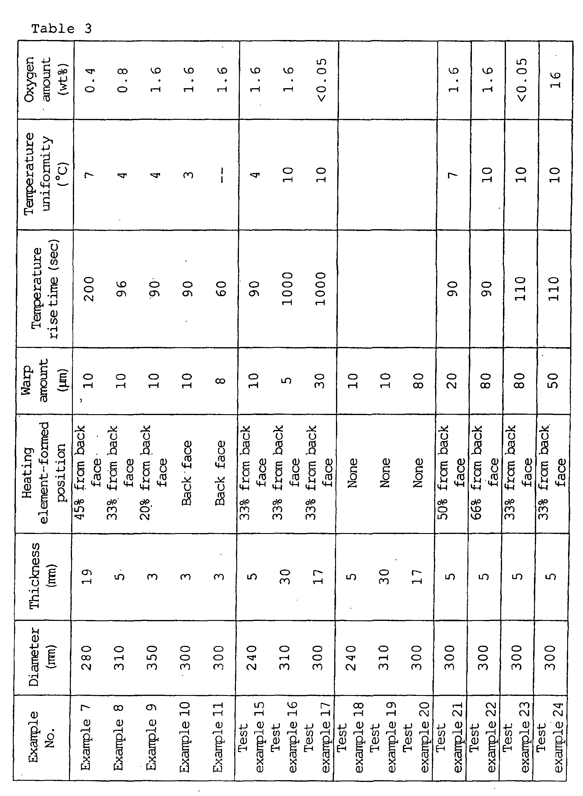 As is clear from the results shown in Tables 1 to 4, the ceramic substrates of the hot plates and the like according to the examples took short temperature rise times and superior in both the temperature-following property and the temperature uniformity. Furthermore, the warp amount at a high temperature can be made small.