EP1189067A2 - A semiconductor device provided with a built-in minute charge detecting circuit - Google Patents
A semiconductor device provided with a built-in minute charge detecting circuit Download PDFInfo
- Publication number
- EP1189067A2 EP1189067A2 EP01122216A EP01122216A EP1189067A2 EP 1189067 A2 EP1189067 A2 EP 1189067A2 EP 01122216 A EP01122216 A EP 01122216A EP 01122216 A EP01122216 A EP 01122216A EP 1189067 A2 EP1189067 A2 EP 1189067A2
- Authority
- EP
- European Patent Office
- Prior art keywords
- charge
- capacitance
- minute
- switch
- detecting circuit
- Prior art date
- Legal status (The legal status is an assumption and is not a legal conclusion. Google has not performed a legal analysis and makes no representation as to the accuracy of the status listed.)
- Granted
Links
- 239000004065 semiconductor Substances 0.000 title claims abstract description 59
- 230000001131 transforming effect Effects 0.000 claims abstract description 51
- 238000012360 testing method Methods 0.000 claims abstract description 34
- 238000007599 discharging Methods 0.000 abstract description 19
- 238000001514 detection method Methods 0.000 abstract description 5
- 238000005259 measurement Methods 0.000 description 24
- 238000010586 diagram Methods 0.000 description 10
- 238000007689 inspection Methods 0.000 description 10
- 238000010276 construction Methods 0.000 description 7
- 238000012545 processing Methods 0.000 description 6
- 230000009467 reduction Effects 0.000 description 4
- 230000006872 improvement Effects 0.000 description 3
- 238000004519 manufacturing process Methods 0.000 description 2
- 239000000523 sample Substances 0.000 description 2
- 238000005070 sampling Methods 0.000 description 2
- 230000008901 benefit Effects 0.000 description 1
- 239000003990 capacitor Substances 0.000 description 1
- 230000007423 decrease Effects 0.000 description 1
- 230000000694 effects Effects 0.000 description 1
- 238000000034 method Methods 0.000 description 1
- 238000012986 modification Methods 0.000 description 1
- 230000004048 modification Effects 0.000 description 1
- 230000008569 process Effects 0.000 description 1
- 230000006641 stabilisation Effects 0.000 description 1
- 238000011105 stabilization Methods 0.000 description 1
Images





Classifications
-
- G—PHYSICS
- G01—MEASURING; TESTING
- G01R—MEASURING ELECTRIC VARIABLES; MEASURING MAGNETIC VARIABLES
- G01R31/00—Arrangements for testing electric properties; Arrangements for locating electric faults; Arrangements for electrical testing characterised by what is being tested not provided for elsewhere
- G01R31/28—Testing of electronic circuits, e.g. by signal tracer
- G01R31/2851—Testing of integrated circuits [IC]
- G01R31/2884—Testing of integrated circuits [IC] using dedicated test connectors, test elements or test circuits on the IC under test
-
- G—PHYSICS
- G01—MEASURING; TESTING
- G01R—MEASURING ELECTRIC VARIABLES; MEASURING MAGNETIC VARIABLES
- G01R29/00—Arrangements for measuring or indicating electric quantities not covered by groups G01R19/00 - G01R27/00
- G01R29/24—Arrangements for measuring quantities of charge
Definitions
- the present invention relates to a semiconductor device provided with a built-in minute charge detecting circuit.
- a semiconductor device provided with a built-in minute charge detecting circuit for detecting a minute electric charge.
- a minute charge generating circuit that serves as an input signal source is arranged near an input terminal of the semiconductor device so as to make an input signal less susceptible to influence of stray capacitance, external noises and the like.
- An output signal of the minute charge detecting circuit is measured with a minute electric charge given as a signal directly to the input terminal so as to measure the gain, the signal-to-noise ratio or the like of the minute charge detecting circuit.
- Fig. 7 shows a semiconductor device 40 with the built-in minute charge detecting circuit and a minute charge generating circuit 50 for inspecting the semiconductor device.
- this semiconductor device has a differential amplifier OP, a charge detecting capacitance C1, a charge-discharging switch SW1 and a processing circuit 44.
- An inverted input terminal of the differential amplifier OP is connected to an input terminal 41 and a non-inverted input terminal of the differential amplifier OP is connected to a ground GND.
- the charge detecting capacitance C1 is connected across an output terminal of the differential amplifier OP and the inverted input terminal of the differential amplifier OP.
- the charge-discharging switch SW1 is connected across the output terminal the differential amplifier OP and the inverted input terminal of the differential amplifier OP.
- the processing circuit 44 processes an output voltage outputted from the differential amplifier OP.
- the differential amplifier OP, the charge detecting capacitance C1 and the charge-discharging switch SW1 constitute a minute charge detecting circuit 43.
- the semiconductor device 40 shown in Fig. 7 is inspected by inputting an electric charge generated in the minute charge generating circuit 50 to the input terminal 41 of the semiconductor device 40.
- the stray capacitance Cf due to wiring is added to the input section of the minute charge detecting circuit 43 even if the minute charge generating circuit 50 is arranged near the minute charge detecting circuit 43 to be measured. Furthermore, in order to connect the minute charge detecting circuit 43 to be measured to the minute charge generating circuit 50 that generates an input signal, it is required to provide a connection by means of a socket or probing. Due to addition of the stray capacitance in the connection, the stray capacitance Cf increases to the extent of several picofarads.
- the accumulated electric charge Qf increases, which decreases the electric charge Q1 accumulated in the charge detecting capacitance C1 of the minute charge detecting circuit 43.
- a measurement error of gain is increased.
- it is required to provide a setting of: Cf ⁇ C1.
- the charge detecting capacitance C1 cannot be increased in the semiconductor device in which the capacitance value of the charge detecting capacitance C1 amounts to several picofarads in order to obtain a sufficient output voltage. Therefore, the measurement accuracy cannot be increased.
- An object of the present invention is to provide a semiconductor device capable of improving accuracy in measurement of a minute charge detecting circuit by suppressing influence of stray capacitance, external noises and the like during test.
- the present invention provides a semiconductor device a semiconductor device comprising: a minute charge detecting circuit for detecting a minute electric charge; and a test circuit provided between an input terminal of the semiconductor device and an input section of the minute charge detecting circuit, the test circuit having: a charge transforming capacitance for transforming a voltage signal inputted from the input terminal into an electric charge, and an operation mode switchover means for switching over between a normal operation mode in which an electric charge inputted to the input terminal is detected by the minute charge detecting circuit and a test operation mode in which the voltage signal inputted to the input terminal is transformed into an electric charge by the charge transforming capacitance and the transformed electric charge is detected by the minute charge detecting circuit.
- the charge transforming capacitance (capacitor) and the operation mode switchover means are provided between the input section of the minute charge detecting circuit and the input terminal of the semiconductor device, and the charge transforming capacitance eliminates the harmful influence of stray capacitance and external noises added to the input terminal.
- the voltage signal from the input signal source of low output impedance can be used as an input signal, and therefore the impedance of the input signal line can be reduced. This arrangement is less susceptible to the influence of the external noises and allows the measurement value to be stabilized.
- the minute charge generating circuit which requires careful handling due to a signal of a minute electric charge, is built in the semiconductor device, and therefore an external inspection circuit is allowed to have a simple construction.
- the operation mode switchover means comprises: a first switch that has one terminal connected to the input terminal and other terminal connected to the input section of the minute charge detecting circuit; and a second switch that has one terminal connected to the charge transforming capacitance and other terminal connected to the input section of the minute charge detecting circuit.
- the operation mode switchover means has the first and second switches to easily switch over between the normal operation mode and the test operation mode.
- the test operation mode of turning off the first switch and turning on the second switch the voltage signal inputted to the input terminal is transformed into an electric charge by the charge transforming capacitance, so that the transformed electric charge is detected by the minute charge detecting circuit.
- the operation mode switchover means comprises: a first switch that has one terminal connected to the input terminal and other terminal connected to the input section of the minute charge detecting circuit; and a second switch that has one terminal connected to the input terminal and other terminal connected to the charge transforming capacitance.
- This embodiment has the same operational advantage as that of the previous embodiment.
- the operation mode switchover means comprises: a first switch that has one terminal connected to the input terminal and other terminal connected to the input section of the minute charge detecting circuit; a second switch that has one terminal connected to the input terminal and other terminal connected to the charge transforming capacitance; and a third switch that has one terminal connected to the charge transforming capacitance and other terminal connected to the input section of the minute charge detecting circuit.
- the semiconductor device of the above-mentioned embodiment when turning off the first switch and turning on the second and third switches, the voltage signal inputted to the input terminal is transformed into an electric charge by the charge transforming capacitance.
- the transformed electric charge is detected by the minute charge detecting circuit. Furthermore, input of unnecessary signals are prevented by selectively turning on the second switch under a state that the first switch is turned off and the third switch is turned on only when the voltage signal for test is applied to the input terminal.
- the second switch is turned on during a period when an electric charge for test use is given to the minute charge detecting circuit and the second switch is turned off during a period when no electric charge for test use is given to the minute charge detecting circuit in a state that the first and third switches are turned on in the test operation mode.
- the second switch is turned on during the period under the state that the first and third switches are turned on when the electric charge for test use is given to the minute charge detecting circuit.
- the second switch is turned off during the period when the electric charge for test use is not given to the minute charge detecting circuit.
- Fig. 1 shows a circuit diagram of a semiconductor device with a built-in minute charge detecting circuit according to a first embodiment of the present invention.
- This semiconductor inspecting device has a charge transforming capacitance Ct whose one terminal is connected to an input terminal 11, a second switch M2 whose one terminal is connected to the other terminal of the charge transforming capacitance Ct, a first switch M1 connected across the other terminal of the second switch M2 and the input terminal 11, a differential amplifier OP whose inverted input terminal is connected to the other terminal of the second switch M2 and whose non-inverted input terminal is connected to a ground GND, a charge detecting capacitance C1 connected across the output terminal of the differential amplifier OP and the inverted input terminal of the differential amplifier OP, a charge-discharging switch SW1 connected across the output terminal of the differential amplifier OP and the inverted input terminal of the differential amplifier OP, and a processing circuit 4 for processing an output signal outputted from the differential amplifier OP.
- a test circuit 2 is constructed of the charge transforming capacitance Ct and the first and second switches M1 and M2.
- a minute charge detecting circuit 3 is constructed of the differential amplifier OP, the charge detecting capacitance C1 and the charge-discharging switch SW1.
- An operation mode switchover means is constructed of the first and second switches M1 and M2.
- a test operation mode firstly, the first switch M1 and the charge-discharging switch SW1 are turned off and the second switch M2 is turned on. In this state, an input voltage signal S1 from the input signal source 1 is applied to the input terminal 11. Then, the first switch M1 and the charge-discharging switch SW1 are turned on to reset the charge quantities of the charge transforming capacitance Ct and the charge detecting capacitance C1. Subsequently, the first switch M1 and the charge-discharging switch SW1 are turned off.
- Measurement of the output voltage Vo at an output voltage measurement terminal 12 enables inspection of the minute charge detecting circuit 3.
- the voltage variation ⁇ Vi of the input voltage signal S1 and the output voltage Vo are determined on the basis of a ratio of a capacitance value of the charge transforming capacitance Ct for transforming the input voltage variation into the minute electric charge with respect to the capacitance value of the charge detecting capacitance C1 of the minute charge detecting circuit 3.
- the capacitance value of the charge transforming capacitance Ct smaller than the capacitance value of the charge detecting capacitance C1
- the voltage value of the voltage variation ⁇ Vi of the input voltage signal S1 for giving the minute electric charge can be increased. Therefore, the fluctuation of the input voltage signal S1 by the influence of the external noises can be reduced, and thereby the inspection accuracy is improved.
- the charge transforming capacitance Ct and the second and third switches M2 and M3 are built within the semiconductor device in this embodiment. Therefore, a stray capacitance added to an input section of the minute charge detecting circuit 3 has a minute capacitance value of only the stray capacitance inside the semiconductor device because no external measurement circuits exert influence on the stray capacitance. Therefore, the input charge quantity given to the minute charge detecting circuit 3 is not reduced by the influence of the external measurement circuits, by which no error occurs in measuring the gain of the minute charge detecting circuit 3.
- test circuit 2 between the input terminal 11 and the minute charge detecting circuit 3
- it is not required to externally input the minute electric charge which is susceptible to the influence of noises during inspection and the external stray capacitance.
- This enables improvement of accuracy in measurement and achievement of stable inspection or test.
- external inspection circuits can also be simplified, so that occurrence of various problems in the mass-production line and the like can also be suppressed.
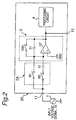
- Fig. 2 is a circuit diagram of a semiconductor device with a built-in minute charge detecting circuit according to a second embodiment of the present invention.
- This semiconductor inspecting device has the same construction as that of the semiconductor inspecting device of the first embodiment except for the position where the second switch M2 is connected.
- the same components as those of the first embodiment are denoted by the same reference numerals and no description is provided for them.
- a second switch M2 of the second embodiment is arranged between an input terminal 11 and a charge transforming capacitance Ct while the second switch M2 of the first embodiment is arranged between the charge transforming capacitance Ct and the input section of the minute charge detecting circuit 3.
- one terminal of the second switch M2 is connected to the input terminal 11 and the other terminal of the second switch M2 is connected to one terminal of the charge transforming capacitance Ct as shown in Fig. 2.
- a test circuit 2A is constructed of the charge transforming capacitance Ct, a first switch M1 and the second switch M2.
- the semiconductor device of this second embodiment has operations and effects similar to those of the semiconductor device of the first embodiment.
- Fig. 3 is a circuit diagram of a semiconductor device with a built-in minute charge detecting circuit according to a third embodiment of the present invention.
- This semiconductor inspecting device is formed in combination of the semiconductor inspecting devices according to the first and second embodiments.
- the same components as those of the first and second embodiments are denoted by the same reference numerals and no description is provided for them.
- This semiconductor inspecting device has a second switch M2 whose one terminal is connected to an input terminal 11, a charge transforming capacitance Ct whose one terminal is connected to the other terminal of the second switch M2, a switch M3 whose one terminal is connected to the other terminal of the charge transforming capacitance Ct, a first switch M1 connected across the other terminal of the switch M3 and the input terminal 11, a differential amplifier OP whose inverted input terminal is connected to the other terminal of the switch M3 and whose non-inverted input terminal is connected to a ground GND, a charge detecting capacitance C1 connected across an output terminal of the differential amplifier OP and the inverted input terminal of the differential amplifier OP, and a charge-discharging switch SW1 connected across the output terminal of the differential amplifier OP and the inverted input terminal of the differential amplifier OP.
- a test circuit 2B is constructed of the charge transforming capacitance Ct and the first, second and third switches M1, M2 and M3.
- a minute charge detecting circuit 3 is constructed of the differential amplifier OP, the charge detecting capacitance C1 and the charge-discharging switch SW1.
- An operation mode switchover means is constructed of the first, second and third switches M1, M2 and M3. It is to be noted that a processing circuit for processing an output voltage outputted from the differential amplifier OP is not shown.
- the first switch M1 is turned on in a state that the second and third switches M2, M3 and the charge-discharging switch SW1 are turned off as shown in Fig. 4, and thereby the electric charge signal Q1 is directly given from the input signal source 1 to the charge detecting capacitance C1.
- An electric charge of the charge detecting capacitance C1 is discharged by turning on the charge-discharging switch SW1.
- the minute charge detecting circuit 3 is initialized to establish a measurement state of a next electric charge. As described above, even with the built-in test circuit 2B, the minute charge detection in the normal operation mode can be achieved.
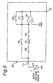
- the first switch M1 and the charge-discharging switch SW1 are turned off and the second and third switches M2 and M3 are turned on as shown in Fig. 5.
- an input voltage signal S1 from the input signal source 1 is applied to the input terminal 11.
- the first switch M1 and the charge-discharging switch SW1 are turned on to reset the charge quantities of the charge transforming capacitance Ct and the charge detecting capacitance C1.
- the first switch M1 and the charge-discharging switch SW1 are turned off.
- a voltage variation ⁇ Vi of the input voltage signal S1 obtained after the resetting is transformed into an electric charge Qi by the charge transforming capacitance Ct.
- Measurement of the output voltage Vo at an output voltage measurement terminal 12 enables inspection of the minute charge detecting circuit 3.
- the voltage variation ⁇ Vi of the input voltage signal S1 and the output voltage Vo are determined on the basis of a ratio of a capacitance value of the charge transforming capacitance Ct for transforming the input voltage variation into the minute electric charge with respect to the capacitance value of the charge detecting capacitance C1 of the minute charge detecting circuit 3.
- the capacitance value of the charge transforming capacitance Ct smaller than the capacitance value of the charge detecting capacitance C1
- the voltage value of the voltage variation ⁇ Vi of the input voltage signal S1 for giving the minute electric charge can be increased. Therefore, the fluctuation of the input voltage signal S1 by the influence of the external noises can be reduced, and thereby the inspection accuracy is improved.
- the charge transforming capacitance Ct and the second and third switches M2 and M3 are built within the semiconductor device in this embodiment. Therefore, a stray capacitance added to an input section of the minute charge detecting circuit 3 has a minute capacitance value of only the stray capacitance inside the semiconductor device because no external measurement circuits exert influence on the stray capacitance. Therefore, the input charge quantity given to the minute charge detecting circuit 3 is not reduced by the influence of the external measurement circuits, by which no error occurs in measuring the gain of the minute charge detecting circuit 3.
- the semiconductor device provided with the minute charge detecting circuit 3 which is constructed of the differential amplifier OP, the charge detecting capacitance C1 and the charge-discharging switch SW1.
- construction of the minute charge detecting circuit is not limited to the above-mentioned.
- the operation mode switchover means is constructed of the first and second switches M1 and M2.
- the operation mode switchover means is constructed of the first, second and third switches M1, M2 and M3.
- the operation mode switchover means is not limited to those.
- the operation mode switchover means may have any other circuit constructions if they can switch over between the normal operation mode in which the electric charge inputted to the input terminal is detected by the minute charge detecting circuit and the test operation mode in which the voltage signal inputted to the input terminal is transformed into an electric charge by the charge transforming capacitance and the transformed electric charge is detected by the minute charge detecting circuit.
- the semiconductor device of the present invention by integrating the test circuit into the semiconductor inspecting device provided with the minute charge detecting circuit, the influence of the stray capacitance due to the external measurement circuit can be eliminated, and the external input signal can be reduced in impedance for the reduction in the influence of the measurement signal or the external noises.
- the above arrangement enables stabilization of measurement level and improvement of measurement accuracy.
- the above arrangement also enables simplification of external measurement circuits and reduction of troubles in mass-production.
Landscapes
- Physics & Mathematics (AREA)
- General Physics & Mathematics (AREA)
- Engineering & Computer Science (AREA)
- Computer Hardware Design (AREA)
- Microelectronics & Electronic Packaging (AREA)
- General Engineering & Computer Science (AREA)
- Tests Of Electronic Circuits (AREA)
- Semiconductor Integrated Circuits (AREA)
- Amplifiers (AREA)
- Testing Or Measuring Of Semiconductors Or The Like (AREA)
Abstract
Description
Claims (5)
- A semiconductor device comprising:a minute charge detecting circuit (3) for detecting a minute electric charge; anda test circuit provided between an input terminal (11) of the semiconductor device (10, 20, 30) and an input section of the minute charge detecting circuit (3), the test circuit (2, 2A, 2B) having:a charge transforming capacitance (Ct) for transforming a voltage signal inputted from the input terminal (11) into an electric charge; andan operation mode switchover means for switching over between a normal operation mode in which an electric charge inputted to the input terminal (11) is detected by the minute charge detecting circuit (3) and a test operation mode in which the voltage signal inputted to the input terminal (11) is transformed into an electric charge by the charge transforming capacitance (Ct) and the transformed electric charge is detected by the minute charge detecting circuit (3).
- A semiconductor device as set forth in claim 1, wherein
the operation mode switchover means comprises:a first switch (M1) that has one terminal connected to the input terminal (11) and other terminal connected to the input section of the minute charge detecting circuit (3); anda second switch (M2) that has one terminal connected to the charge transforming capacitance (Ct) and other terminal connected to the input section of the minute charge detecting circuit (3). - A semiconductor device as set forth in claim 1, wherein
the operation mode switchover means comprises:a first switch (M1) that has one terminal connected to the input terminal (11) and other terminal connected to the input section of the minute charge detecting circuit (3); anda second switch (M2) that has one terminal connected to the input terminal (11) and other terminal connected to the charge transforming capacitance (Ct). - A semiconductor device as set forth in claim 1, wherein
the operation mode switchover means comprises:a first switch (M1) that has one terminal connected to the input terminal (11) and other terminal connected to the input section of the minute charge detecting circuit (3);a second switch (M2) that has one terminal connected to the input terminal (11) and other terminal connected to the charge transforming capacitance (Ct); anda third switch (M3) that has one terminal connected to the charge transforming capacitance (Ct) and other terminal connected to the input section of the minute charge detecting circuit (3). - A semiconductor device as set forth in claim 4, wherein
the second switch (M2) is turned on during a period when an electric charge for test use is given to the minute charge detecting circuit (3) and the second switch (M2) is turned off during a period when no electric charge for test use is given to the minute charge detecting circuit (3) in a state that the first and third switches (M1, M3) are turned on in the test operation mode.
Applications Claiming Priority (2)
| Application Number | Priority Date | Filing Date | Title |
|---|---|---|---|
| JP2000281720A JP3584205B2 (en) | 2000-09-18 | 2000-09-18 | Semiconductor device |
| JP2000281720 | 2000-09-18 |
Publications (3)
| Publication Number | Publication Date |
|---|---|
| EP1189067A2 true EP1189067A2 (en) | 2002-03-20 |
| EP1189067A3 EP1189067A3 (en) | 2003-09-17 |
| EP1189067B1 EP1189067B1 (en) | 2004-12-29 |
Family
ID=18766334
Family Applications (1)
| Application Number | Title | Priority Date | Filing Date |
|---|---|---|---|
| EP01122216A Expired - Lifetime EP1189067B1 (en) | 2000-09-18 | 2001-09-17 | A semiconductor device provided with a built-in minute charge detecting circuit |
Country Status (4)
| Country | Link |
|---|---|
| US (1) | US6365914B1 (en) |
| EP (1) | EP1189067B1 (en) |
| JP (1) | JP3584205B2 (en) |
| DE (1) | DE60108023T2 (en) |
Families Citing this family (3)
| Publication number | Priority date | Publication date | Assignee | Title |
|---|---|---|---|---|
| JP4420156B2 (en) * | 2000-06-14 | 2010-02-24 | 日本電気株式会社 | Semiconductor device |
| GB2420458B (en) * | 2004-11-19 | 2008-09-17 | Matsushita Electric Industrial Co Ltd | Envelope detector circuit |
| US8154275B2 (en) * | 2009-07-15 | 2012-04-10 | Apple Inc. | Apparatus and method for testing sense amplifier thresholds on an integrated circuit |
Family Cites Families (10)
| Publication number | Priority date | Publication date | Assignee | Title |
|---|---|---|---|---|
| US4532442A (en) * | 1981-10-23 | 1985-07-30 | Black Ian A | Noise reduction in electronic measuring circuits |
| JPS5885479A (en) | 1981-11-17 | 1983-05-21 | 株式会社東芝 | Route display |
| JPH0738545B2 (en) * | 1988-05-12 | 1995-04-26 | 株式会社村田製作所 | Signal generation circuit for charge generation type sensing element |
| US5206500A (en) * | 1992-05-28 | 1993-04-27 | Cincinnati Microwave, Inc. | Pulsed-laser detection with pulse stretcher and noise averaging |
| US5543728A (en) * | 1993-06-15 | 1996-08-06 | Grace; James W. | Low leakage diode switches for a tester circuit for integrated circuits |
| DE19506134B4 (en) * | 1994-03-04 | 2005-08-25 | Volkswagen Ag | charge amplifier |
| JP3171373B2 (en) * | 1995-10-12 | 2001-05-28 | アルプス電気株式会社 | Microcurrent detection circuit and coordinate input device using the same |
| DK0834992T3 (en) * | 1996-10-02 | 1999-09-13 | Kavlico Corp | Monolithic MOS switched-capacitor circuit with on-chip oscillator |
| US5838241A (en) * | 1996-12-18 | 1998-11-17 | Robertshaw Controls Company | Liquid level transmitter |
| JP4042069B2 (en) * | 1996-12-26 | 2008-02-06 | 聯華電子股▲分▼有限公司 | Integral input type input circuit and test method thereof |
-
2000
- 2000-09-18 JP JP2000281720A patent/JP3584205B2/en not_active Expired - Fee Related
-
2001
- 2001-09-17 EP EP01122216A patent/EP1189067B1/en not_active Expired - Lifetime
- 2001-09-17 DE DE60108023T patent/DE60108023T2/en not_active Expired - Lifetime
- 2001-09-18 US US09/954,059 patent/US6365914B1/en not_active Expired - Lifetime
Also Published As
| Publication number | Publication date |
|---|---|
| DE60108023T2 (en) | 2005-12-15 |
| US6365914B1 (en) | 2002-04-02 |
| JP3584205B2 (en) | 2004-11-04 |
| JP2002090430A (en) | 2002-03-27 |
| EP1189067A3 (en) | 2003-09-17 |
| US20020033482A1 (en) | 2002-03-21 |
| EP1189067B1 (en) | 2004-12-29 |
| DE60108023D1 (en) | 2005-02-03 |
Similar Documents
| Publication | Publication Date | Title |
|---|---|---|
| US8508217B2 (en) | Output circuit of charge mode sensor | |
| US7129487B2 (en) | Infrared detecting circuit and an infrared detector | |
| US5959463A (en) | Semiconductor test apparatus for measuring power supply current of semiconductor device | |
| US8228054B2 (en) | Method and apparatus for amplifying a signal and test device using same | |
| JPH1054851A (en) | Instrument for measuring output current of power source | |
| US7023223B2 (en) | Impedance measuring circuit and capacitance measuring circuit | |
| EP1426772B1 (en) | Impedance measuring circuit, its method, and capacitance measuring circuit | |
| TWI408378B (en) | Apparatus for current sensing | |
| EP1424562A1 (en) | Sensor capacity sensing apparatus and sensor capacity sensing method | |
| JPH04212067A (en) | Dual-path wide-band high-precision data collecting system | |
| US6365914B1 (en) | Semiconductor device provided with a built-in minute charge detecting circuit | |
| US8175824B2 (en) | Circuit testing apparatus | |
| US7026844B2 (en) | Sensor signal detection device | |
| JP6718284B2 (en) | Signal processing circuit, coulomb counter circuit, electronic device | |
| JPS6325572A (en) | Leakage current measuring system of electrometer amplifier | |
| JP3311464B2 (en) | Signal measurement device | |
| JP4735250B2 (en) | Measuring device | |
| JP3821057B2 (en) | Two-terminal circuit element measuring apparatus and contact check method | |
| US7489153B2 (en) | Semiconductor memory device | |
| CN115184686A (en) | Capacitance test circuit and circuit board | |
| JP2004200979A (en) | Semiconductor integrated circuit | |
| KR19980034681A (en) | In Circuit Tester | |
| JPH074598Y2 (en) | Measuring terminal structure of digital capacitance meter | |
| Castro et al. | Precision Signal Conditioning for High Resolution Industrial Applications | |
| JPS63205573A (en) | Direct-reading accurate digital capacity meter |
Legal Events
| Date | Code | Title | Description |
|---|---|---|---|
| PUAI | Public reference made under article 153(3) epc to a published international application that has entered the european phase |
Free format text: ORIGINAL CODE: 0009012 |
|
| AK | Designated contracting states |
Kind code of ref document: A2 Designated state(s): AT BE CH CY DE DK ES FI FR GB GR IE IT LI LU MC NL PT SE TR |
|
| AX | Request for extension of the european patent |
Free format text: AL;LT;LV;MK;RO;SI |
|
| PUAL | Search report despatched |
Free format text: ORIGINAL CODE: 0009013 |
|
| AK | Designated contracting states |
Kind code of ref document: A3 Designated state(s): AT BE CH CY DE DK ES FI FR GB GR IE IT LI LU MC NL PT SE TR |
|
| AX | Request for extension of the european patent |
Extension state: AL LT LV MK RO SI |
|
| 17P | Request for examination filed |
Effective date: 20040123 |
|
| 17Q | First examination report despatched |
Effective date: 20040220 |
|
| AKX | Designation fees paid |
Designated state(s): DE FR GB |
|
| GRAP | Despatch of communication of intention to grant a patent |
Free format text: ORIGINAL CODE: EPIDOSNIGR1 |
|
| GRAS | Grant fee paid |
Free format text: ORIGINAL CODE: EPIDOSNIGR3 |
|
| GRAA | (expected) grant |
Free format text: ORIGINAL CODE: 0009210 |
|
| AK | Designated contracting states |
Kind code of ref document: B1 Designated state(s): DE FR GB |
|
| REG | Reference to a national code |
Ref country code: GB Ref legal event code: FG4D |
|
| REG | Reference to a national code |
Ref country code: IE Ref legal event code: FG4D |
|
| REF | Corresponds to: |
Ref document number: 60108023 Country of ref document: DE Date of ref document: 20050203 Kind code of ref document: P |
|
| ET | Fr: translation filed | ||
| PLBE | No opposition filed within time limit |
Free format text: ORIGINAL CODE: 0009261 |
|
| STAA | Information on the status of an ep patent application or granted ep patent |
Free format text: STATUS: NO OPPOSITION FILED WITHIN TIME LIMIT |
|
| 26N | No opposition filed |
Effective date: 20050930 |
|
| REG | Reference to a national code |
Ref country code: FR Ref legal event code: PLFP Year of fee payment: 15 |
|
| PGFP | Annual fee paid to national office [announced via postgrant information from national office to epo] |
Ref country code: DE Payment date: 20150922 Year of fee payment: 15 Ref country code: GB Payment date: 20150917 Year of fee payment: 15 |
|
| PGFP | Annual fee paid to national office [announced via postgrant information from national office to epo] |
Ref country code: FR Payment date: 20150922 Year of fee payment: 15 |
|
| REG | Reference to a national code |
Ref country code: DE Ref legal event code: R119 Ref document number: 60108023 Country of ref document: DE |
|
| GBPC | Gb: european patent ceased through non-payment of renewal fee |
Effective date: 20160917 |
|
| REG | Reference to a national code |
Ref country code: FR Ref legal event code: ST Effective date: 20170531 |
|
| PG25 | Lapsed in a contracting state [announced via postgrant information from national office to epo] |
Ref country code: DE Free format text: LAPSE BECAUSE OF NON-PAYMENT OF DUE FEES Effective date: 20170401 Ref country code: GB Free format text: LAPSE BECAUSE OF NON-PAYMENT OF DUE FEES Effective date: 20160917 Ref country code: FR Free format text: LAPSE BECAUSE OF NON-PAYMENT OF DUE FEES Effective date: 20160930 |