EP1187166B1 - Plasma display panel and method for manufacturing the same - Google Patents
Plasma display panel and method for manufacturing the same Download PDFInfo
- Publication number
- EP1187166B1 EP1187166B1 EP01301155A EP01301155A EP1187166B1 EP 1187166 B1 EP1187166 B1 EP 1187166B1 EP 01301155 A EP01301155 A EP 01301155A EP 01301155 A EP01301155 A EP 01301155A EP 1187166 B1 EP1187166 B1 EP 1187166B1
- Authority
- EP
- European Patent Office
- Prior art keywords
- partition
- horizontal
- walls
- display panel
- plasma display
- Prior art date
- Legal status (The legal status is an assumption and is not a legal conclusion. Google has not performed a legal analysis and makes no representation as to the accuracy of the status listed.)
- Expired - Lifetime
Links
- 238000000034 method Methods 0.000 title claims description 21
- 238000004519 manufacturing process Methods 0.000 title claims description 8
- 238000005192 partition Methods 0.000 claims description 108
- 239000000758 substrate Substances 0.000 claims description 41
- 239000000463 material Substances 0.000 claims description 30
- 229910052751 metal Inorganic materials 0.000 claims description 22
- 239000002184 metal Substances 0.000 claims description 22
- 239000011521 glass Substances 0.000 claims description 15
- 238000002844 melting Methods 0.000 claims description 10
- 230000008018 melting Effects 0.000 claims description 10
- 239000011159 matrix material Substances 0.000 claims description 4
- 238000000059 patterning Methods 0.000 claims description 2
- 230000008569 process Effects 0.000 description 11
- 238000010586 diagram Methods 0.000 description 6
- 239000003086 colorant Substances 0.000 description 4
- 239000002131 composite material Substances 0.000 description 4
- 239000004020 conductor Substances 0.000 description 4
- 102100039169 [Pyruvate dehydrogenase [acetyl-transferring]]-phosphatase 1, mitochondrial Human genes 0.000 description 3
- 101710126534 [Pyruvate dehydrogenase [acetyl-transferring]]-phosphatase 1, mitochondrial Proteins 0.000 description 3
- 239000000203 mixture Substances 0.000 description 3
- UQSXHKLRYXJYBZ-UHFFFAOYSA-N Iron oxide Chemical compound [Fe]=O UQSXHKLRYXJYBZ-UHFFFAOYSA-N 0.000 description 2
- VYPSYNLAJGMNEJ-UHFFFAOYSA-N Silicium dioxide Chemical compound O=[Si]=O VYPSYNLAJGMNEJ-UHFFFAOYSA-N 0.000 description 2
- 230000008901 benefit Effects 0.000 description 2
- 230000015572 biosynthetic process Effects 0.000 description 2
- 238000005520 cutting process Methods 0.000 description 2
- 239000007787 solid Substances 0.000 description 2
- CIWBSHSKHKDKBQ-JLAZNSOCSA-N Ascorbic acid Chemical compound OC[C@H](O)[C@H]1OC(=O)C(O)=C1O CIWBSHSKHKDKBQ-JLAZNSOCSA-N 0.000 description 1
- VYZAMTAEIAYCRO-UHFFFAOYSA-N Chromium Chemical compound [Cr] VYZAMTAEIAYCRO-UHFFFAOYSA-N 0.000 description 1
- CPLXHLVBOLITMK-UHFFFAOYSA-N Magnesium oxide Chemical compound [Mg]=O CPLXHLVBOLITMK-UHFFFAOYSA-N 0.000 description 1
- 230000002411 adverse Effects 0.000 description 1
- PNEYBMLMFCGWSK-UHFFFAOYSA-N aluminium oxide Inorganic materials [O-2].[O-2].[O-2].[Al+3].[Al+3] PNEYBMLMFCGWSK-UHFFFAOYSA-N 0.000 description 1
- 229910052804 chromium Inorganic materials 0.000 description 1
- 239000011651 chromium Substances 0.000 description 1
- 229910052681 coesite Inorganic materials 0.000 description 1
- 229910052593 corundum Inorganic materials 0.000 description 1
- 229910052906 cristobalite Inorganic materials 0.000 description 1
- 230000007423 decrease Effects 0.000 description 1
- 238000001035 drying Methods 0.000 description 1
- 230000005611 electricity Effects 0.000 description 1
- 239000000945 filler Substances 0.000 description 1
- 238000000227 grinding Methods 0.000 description 1
- 238000010438 heat treatment Methods 0.000 description 1
- 230000006872 improvement Effects 0.000 description 1
- 238000010030 laminating Methods 0.000 description 1
- WPBNNNQJVZRUHP-UHFFFAOYSA-L manganese(2+);methyl n-[[2-(methoxycarbonylcarbamothioylamino)phenyl]carbamothioyl]carbamate;n-[2-(sulfidocarbothioylamino)ethyl]carbamodithioate Chemical compound [Mn+2].[S-]C(=S)NCCNC([S-])=S.COC(=O)NC(=S)NC1=CC=CC=C1NC(=S)NC(=O)OC WPBNNNQJVZRUHP-UHFFFAOYSA-L 0.000 description 1
- 230000000873 masking effect Effects 0.000 description 1
- 238000012986 modification Methods 0.000 description 1
- 230000004048 modification Effects 0.000 description 1
- 230000003287 optical effect Effects 0.000 description 1
- 239000003973 paint Substances 0.000 description 1
- 238000000206 photolithography Methods 0.000 description 1
- 239000000843 powder Substances 0.000 description 1
- 230000004044 response Effects 0.000 description 1
- 238000007650 screen-printing Methods 0.000 description 1
- 238000007789 sealing Methods 0.000 description 1
- 239000000377 silicon dioxide Substances 0.000 description 1
- 125000006850 spacer group Chemical group 0.000 description 1
- 229910052682 stishovite Inorganic materials 0.000 description 1
- 230000001629 suppression Effects 0.000 description 1
- 229910052905 tridymite Inorganic materials 0.000 description 1
- 230000000007 visual effect Effects 0.000 description 1
- 239000002699 waste material Substances 0.000 description 1
- 229910001845 yogo sapphire Inorganic materials 0.000 description 1
Images






Classifications
-
- H—ELECTRICITY
- H01—ELECTRIC ELEMENTS
- H01J—ELECTRIC DISCHARGE TUBES OR DISCHARGE LAMPS
- H01J9/00—Apparatus or processes specially adapted for the manufacture, installation, removal, maintenance of electric discharge tubes, discharge lamps, or parts thereof; Recovery of material from discharge tubes or lamps
- H01J9/24—Manufacture or joining of vessels, leading-in conductors or bases
- H01J9/241—Manufacture or joining of vessels, leading-in conductors or bases the vessel being for a flat panel display
- H01J9/242—Spacers between faceplate and backplate
-
- H—ELECTRICITY
- H01—ELECTRIC ELEMENTS
- H01J—ELECTRIC DISCHARGE TUBES OR DISCHARGE LAMPS
- H01J11/00—Gas-filled discharge tubes with alternating current induction of the discharge, e.g. alternating current plasma display panels [AC-PDP]; Gas-filled discharge tubes without any main electrode inside the vessel; Gas-filled discharge tubes with at least one main electrode outside the vessel
- H01J11/10—AC-PDPs with at least one main electrode being out of contact with the plasma
- H01J11/12—AC-PDPs with at least one main electrode being out of contact with the plasma with main electrodes provided on both sides of the discharge space
-
- H—ELECTRICITY
- H01—ELECTRIC ELEMENTS
- H01J—ELECTRIC DISCHARGE TUBES OR DISCHARGE LAMPS
- H01J11/00—Gas-filled discharge tubes with alternating current induction of the discharge, e.g. alternating current plasma display panels [AC-PDP]; Gas-filled discharge tubes without any main electrode inside the vessel; Gas-filled discharge tubes with at least one main electrode outside the vessel
- H01J11/20—Constructional details
- H01J11/34—Vessels, containers or parts thereof, e.g. substrates
- H01J11/36—Spacers, barriers, ribs, partitions or the like
-
- H—ELECTRICITY
- H01—ELECTRIC ELEMENTS
- H01J—ELECTRIC DISCHARGE TUBES OR DISCHARGE LAMPS
- H01J2211/00—Plasma display panels with alternate current induction of the discharge, e.g. AC-PDPs
- H01J2211/20—Constructional details
- H01J2211/34—Vessels, containers or parts thereof, e.g. substrates
- H01J2211/36—Spacers, barriers, ribs, partitions or the like
- H01J2211/361—Spacers, barriers, ribs, partitions or the like characterized by the shape
Definitions
- the present invention relates to a plasma display panel (PDP) having a mesh-patterned partition, each square of which encloses one or more cells for constituting a display surface and a method for manufacturing the PDP.
- PDP plasma display panel
- a PDP is commercialized for a wall-hung TV set, whose screen size has reached 60 inches.
- PDP is a digital display device comprising binary light emission cells, so it is suitable for a display of digital data and is expected as a multimedia monitor.
- a new panel structure is under development, which can provide a brighter and more stable display and can be manufactured in a high productivity.
- An AC type PDP for a color display employs a surface discharge format.
- the surface discharge format has an arrangement of electrodes in which display electrodes that become anodes and cathodes in a display discharge for ensuring a luminance are arranged in parallel on a front or back substrate, and address electrodes are arranged so as to cross a pair of the display electrodes.
- a partition is necessary for separating a discharge for each column of a matrix display along the longitudinal direction of the display electrode (hereinafter referred to as the row direction).
- the partition also works as a spacer for defining a discharge space size in the direction of the panel thickness.
- a partition pattern (a shape of the partition in the plan view) is broadly divided into a stripe pattern and a mesh pattern.
- the stripe pattern divides the discharge space for cells arranged in the row direction (i.e., in each column). In the stripe pattern, the discharge space of cell included in each column is not separated, so that exhausting of inner air and filling of discharge gas are relatively easy in a manufacturing process of a PDP.
- the mesh pattern divides the discharge space both in the row direction and in the column direction.
- a typical mesh pattern is a check pattern.
- a mesh pattern has an advantage in that the discharge is separated for each cell and that a fluorescent material is arranged on a side face of the partition so as to enclose the cell for increasing a light emission area.
- the mesh pattern however, has a disadvantage in that a gap generated by subtle unevenness on the upper surface of the partition becomes an air path in the inner air exhaustion, so a resistance of the air exhaustion is large and it takes a long time for the process.
- a partition structure of an overlaying form of the mesh-patterned partition and the stripe-patterned partition (this is called a composite pattern structure) is known.
- this structure since the discharge space is continuous as in the case of the stripe pattern, the air exhaustion resistance is smaller than in the case where the stripe-patterned partition is not overlaid.
- an improved composite pattern structure is disclosed in Japanese unexamined patent publication No. 4-274141 , in which a stripe-patterned partition is provided with a hiatus for each cell, so that a grid-shaped air path (air exhaustion path) is formed for the gas to flow not only in the column direction but also in the row direction.
- the above-explained partition having the composite pattern structure has a mesh-patterned partition whose banding portion in the column direction or the row direction is raised.
- the partition forming process becomes complicated for forming the above-mentioned structure on the inner surface of one of the substrate pair.
- the fluorescent material should be arranged on both of the substrates for increasing the area in which the fluorescent material is formed.
- a registration of the substrate pair in the assembling process is difficult.
- the partition having the composite pattern structure is adverse from the viewpoint of the productivity.
- An object of the present invention is to provide a PDP that has a good productivity of partition formation and air exhaustion process and can display more brightly and more stably than a PDP that has a stripe-patterned partition.
- a plasma display panel comprising: a pair of substrates arranged so as to define a gap therebetween, each substrate having an inner surface bounding said gap; a discharge gas which substantially fills the gap between the substrates; and a mesh-patterned partition arranged on the inner surface of one of the substrates and including respective pluralities of vertical walls and horizontal walls which divide the gap into a plurality of squares corresponding to an arrangement of discharge cells arranged in respective pluralities of rows and columns; characterized in that: the partition is composed of a low melting point glass; and the partition is formed such that at least a portion of a horizontal wall which meets a portion of a vertical wall has a height lower than a height of a remaining portion of the vertical wall, thereby forming an air path in the panel.
- the partition has low portions that form a mesh-like air path that travels all gas-filled space enclosed by the partition in a plan view.
- the portion corresponding to the line along the horizontal direction is made low.
- the pattern width (the line width) of the portion corresponding to the line along the horizontal direction is made thicker than the pattern width of the portion corresponding to the line along the vertical direction so as to generate a height difference.
- the shrink quantity in the thick portion is smaller in the width direction but is larger in the height direction than the thin portion.
- EP-A-0920048 discloses a plasma display panel comprising: a pair of substrates arranged so as to define a gap therebetween, each substrate having an inner surface bounding said gap; a discharge gas which substantially fills the gap between the substrates; and a mesh-patterned partition arranged on the inner surface of one of the substrates and including respective pluralities of vertical walls and horizontal walls which divide the gap into a plurality of squares corresponding to an arrangement of discharge cells arranged in respective pluralities of rows and columns.
- the partition is composed of a low melting point glass formed such that at least a portion of a horizontal wall which meets a portion of a vertical wall has a height lower than a height of a remaining portion of the vertical wall, thereby forming an air path in the panel.
- a method of manufacturing a plasma display panel comprising the steps of : forming a layer made of a partition material having a heat shrink property on one of the substrates, the layer having a constant height; patterning the partition material layer so as to define the mesh-patterned partition including the vertical walls and the horizontal walls thereby to produce a matrix arrangement of a plurality of discharge cells in plural rows and columns that cross each other, each of the horizontal walls having a width larger than that of the vertical walls; and baking the patterned partition material layer in order to form the partition having a portion whose height is reduced in the horizontal wall having the large width.
- Fig. 1 is a diagram showing a cell structure of a PDP according to the present invention.
- Fig. 2 is a plan view showing the arrangement relationship between the display electrode and the partition.
- Fig. 3 is a plan view showing a partition pattern.
- Fig. 4 is a diagram showing a solid structure of the partition.
- Fig. 5 is a schematic diagram showing heat shrink in the partition forming process.
- Fig. 6 is a diagram showing a baking profile in the partition forming process.
- Figs. 7 , 8A and 8B show variations of the partition pattern.
- Figs. 9A-12 show variations of the display electrode pattern.
- Fig. 1 is a diagram showing a cell structure of a PDP according to the present invention.
- Fig. 2 is a plan view showing the arrangement relationship between the display electrode and the partition.
- Fig. 1 is a drawing of an inner structure, which shows a pair of substrate structures being separated from each other.
- the PDP 1 comprises a pair of substrate structures (a structure including a substrate on which cell elements are arranged) 10, 20, and the display surface ES comprises m x n cells.
- the display electrodes X, Y constituting an electrode pair for generating the display discharge are extending in the row direction (the horizontal direction) of the matrix display, and the address electrodes A are extending in the column direction (the vertical direction).
- the display electrodes X, Y are arranged on the inner surface of the glass substrate 11 of the front substrate structure 10 as a pair for each row.
- the "row” means a set of cells whose positions in the column direction are the same, and the number of the cells is equal to the number of columns (m).
- Each of the display electrodes X and Y includes a transparent conductive film 41 that forms a surface discharge gap (a discharge slit) and a metal film (a bus conductor) 42 that is overlaid on the edge in the column direction.
- the display electrodes X, Y are covered with a dielectric layer 17 having the thickness of approximately 20-40 ⁇ m, and the surface of the dielectric layer 17 is coated with a protection film 18 made of magnesia (MgO).
- the electrode gap between rows (that is called a reverse slit) is provided with a dark color layer 65 that is called a black stripe by applying a paint on the outer surface of the glass substrate 11 or by forming a colored glass layer including fillers such as manganese, iron oxide, chromium and other colorant so as to increase contrast (see Fig. 2 ).
- the address electrodes A are arranged on the inner surface of the glass substrate 21 of the back substrate structure 20 as one for each column and are covered with a dielectric layer 24.
- the partition 29 is disposed, which has a grid pattern with partially low profile structure that is unique to the present invention.
- the partition 29 is made of a baked material of a low melting point glass and includes a portion for dividing the discharge space into columns (hereinafter referred to as a vertical wall) 291 and a portion for dividing a discharge space into rows (hereinafter referred to as a horizontal wall) 292.
- the intersection of the vertical wall 291 and the horizontal wall 292 is a common part of them.
- the horizontal wall 292 is lower than the vertical wall 291 by approximately 10 ⁇ m.
- the upper surface of the dielectric layer 24 and the side face of the partition 29 are covered with red, green and blue colors of fluorescent material layers 28R, 28G and 28B for color display.
- the italic letters ( R , G and B ) in Fig. 1 signify light emission colors of the fluorescent materials.
- the color arrangement has a repeating pattern of red, green and blue colors in such a way that the cells in a column have the same color.
- the fluorescent material layers 28R, 28G and 28B are excited by ultraviolet rays generated by the discharge gas in the corresponding cell and emit light.
- the metal film 42 of each of the display electrodes X, Y is overlaid on the partition 29 so as to avoid shading and to blind the partition 29 partially for reducing reflection of external light rays.
- the transparent conductive film 41 is patterned in such a way that the portion for the surface discharge is substantially separated from the portion overlaid on the metal film 42, for suppressing discharge current so as to enhance the efficiency of light emission.
- the portion for the display discharge of the transparent conductive film 41 is separated from the horizontal wall 292 by a distance more than 30 ⁇ m, so that energy loss is largely reduced compared with the case where the distance is less than 30 ⁇ m. It is desirable that the distance between the horizontal wall 292 and the transparent conductive film 41 is set so that the discharge current is reduced by more than 5%.
- the PDP 1 having the above-mentioned structure can be manufactured by the following process.
- Fig. 3 is a plan view showing a partition pattern.
- Fig. 4 is a diagram showing a solid structure of the partition.
- the partition pattern is a grid pattern in which each square of the grid pattern encloses a cell C individually.
- the inter-row portion 293 (the portion between the cells aligned in the column direction) of the partition 29 includes two horizontal walls 292 and a part of the vertical wall 291.
- the plan view pattern of the inter-row portion 293 is made a ladder pattern, and a space 33 is formed between the gas-filled space 32 that corresponds to each of the cells C aligned in the column direction.
- the dielectric constant of the discharge gas is approximately one eighth of that of a low melting point glass that is a common material of the partition, capacitance between the display electrodes of the neighboring rows is reduced, so that a waste of power consumption can be reduced and response of drive control can be improved.
- the side face of the vertical wall 291 and the side face of the horizontal wall 292 respectively are provided with a fluorescent material, so that the light emission area is enlarged and the light emission efficiency can be improved.
- the inter-row portion 293 of the partition 29 is made approximately 10 ⁇ m lower than other portions, thereby forming an air exhaustion path 90 that has a grid shape in the plan view for enabling air exhaustion both in the column direction and in the row direction.
- the width W20 of the inter-row portion 293 is substantially large, and the air exhaustion conductance is substantially the same as the stripe pattern.
- Concrete dimension of the partition 29 is as follows.
- the width W20 of the inter-row portion 293 is substantially larger than the width W11 of the vertical wall 291, so that the difference between the widths makes a height difference between the inter-row portion 293 and other portions.
- the shrink quantity in the height direction depends on the width of the pattern. The shrink can be generated both in the width direction and in the height direction as a whole in the portion 29A having a small pattern width.
- the shrink in the width direction is suppressed more at the portion closer to the center in width direction, so that the shrink is generated more in the height direction compensating the suppression in the width direction. Therefore, the thick portion 29B becomes lower than the thin portion 29A.
- an isotropic shrink occurs in the upper portion of the wall material layer since the shrink can easily occur in any direction, while the shrink in the direction of the substrate surface is suppressed in the bottom portion due to the bond of the substrate. Therefore, the shrink quantity in the height direction becomes larger than the shrink quantity in the direction of the substrate surface.
- the pattern width of the partition is defined as the dimension at the position whose distance from the bottom surface is 10% of the height in this specification. It is desirable that the pattern width of the thick portion is set more than 130% of the pattern width of the thin portion so that a difference of height is generated that is sufficient for air exhaustion.
- the composition of the low melting point glass that is a material of the partition 29 is shown in Table 1.
- Table 1 Composition of the low melting point glass Components Content (wt%) PbO 50-60 B 2 O 3 5-10 SiO 2 10-20 Al 2 O 3 15-25 CaO -5
- the partition 29 it is desirable that it is semitransparent having the absorptance of visual light at approximately 80% per 30 ⁇ m of film thickness. If it is semitransparent, light rays generated at the vicinity of the top of the partition pass the partition and contribute to improvement of the luminance, while external rays that entered the partition are reflected by the bottom surface of the partition and are absorbed by the partition before reaching the front surface. Therefore, a display having a good contrast can be realized.
- the process of forming the partition 29 is as follows.
- Figs. 7 , 8A and 8B show variations of the partition pattern.
- the partition 29b shown in Fig. 7 includes a vertical wall 291 and a horizontal wall 292b.
- the partition 29b corresponds to such that the inter-row portion 293 of the partition 29 shown in Fig. 3 is replaced with the horizontal wall 292b.
- the partition 29c shown in Fig. 8A includes a vertical wall 291c and a horizontal wall 292c.
- the pattern thereof in a plan view is a mesh pattern in which the positions of cells of the neighboring rows are shifted by a half pitch from each other.
- the pattern width of the horizontal wall 292c is set larger than the pattern width of the vertical wall 291c, so that the horizontal wall 292c is lower than the vertical wall 291c, and a mesh-like air exhaustion path 90c is formed.
- the partition 29d shown in Fig. 8B includes a vertical wall 291d and a horizontal wall 292d, and the pattern thereof in a plan view is a honeycomb mesh pattern.
- the pattern width of the zigzag banding horizontal wall 292d is set larger than the pattern width of the vertical wall 291d, so that the horizontal wall 292d is lower than the vertical wall 291d, and a mesh-like air exhaustion path 90d is formed.
- the address electrodes A can be arranged so that the address electrode A weaves in and out of the cells shifted from each other by a half pitch, or that a linear address electrode A is arranged being overlaid on the vertical walls 291c and 291d.
- the display electrodes X, Y can be arranged so that a pair of display electrodes is arranged for each row as shown in Fig. 2 , or that three display electrodes are arranged for two rows as a display electrode is shared by two neighboring rows for display. In any way, the entire bus conductor is overlaid on the horizontal walls 292c and 292d, so that shading can be avoided.
- Figs. 9A-12 show variations of the display electrode pattern.
- Each of the display electrodes Xb and Yb shown in Fig. 9A includes a transparent conductive film 41b and a metal film 42b and corresponds to such display electrodes wherein the pattern of the transparent conductive film 41 of the display electrodes X, Y shown in Fig. 2 is changed.
- the portion of the transparent conductive film 41 to be a discharge surface is connected to the portion that is overlaid on the metal film 42b at the position where it is not overlaid on the vertical wall of the partition 29.
- Each of the display electrodes Xc and Yc shown in Fig. 9B includes a transparent conductive film 41c and a metal film 42c.
- the metal film 42c is arranged at the position where it is not overlaid on the horizontal wall of the partition 29.
- the portion of the transparent conductive film 41d that forms the surface discharge gap to be the discharge surface is divided into columns to be a T-shape.
- the portion of the transparent conductive film 41d that is overlaid on the metal film 42b is straddling over plural columns.
- Each of the display electrodes Xe and Ye shown in Fig. 10B includes a T-shaped transparent conductive film 41e that is divided for each column and a metal film 42b for supplying electricity to the transparent conductive film.
- the structures of Figs. 10A and 10B in which the transparent conductive film is divided are effective for suppressing a discharge current and for reducing a capacitance between electrodes.
- a bus conductor is provided for hiding the reverse slit, so that the process of forming the black stripe can be omitted.
- the partition 29e includes a vertical wall 291 and a horizontal wall 292e and corresponds to such partition wherein the inter-row portion 293 of the partition 29 shown in Fig. 3 is replaced with three horizontal walls 292e.
- the following electrode structure can be applied both to the partition 29 shown in Fig. 2 and to the partition 29b shown in Fig. 7 .
- each of the display electrodes Xf and Yf includes a transparent conductive film 41f and a metal film 42d and is arranged so that the neighboring electrodes of the neighboring rows are the same kind (e.g., in the order of X, Y, Y, X, X, Y, ).
- the transparent conductive film 41f is patterned in the same way as the transparent conductive film 41b shown in Fig. 9A except for the size of the portion that is overlaid on the metal film 42d.
- the display electrodes Xf and Yf have a feature in that the metal film 42d as a bus conductor has a large width over two neighboring horizontal walls 292e.
- the metal film 42d Since an element close to the display surface is drawn at the upper in the figure, a part of the metal film 42d is covered with the transparent conductive film 41f. However, actually in the observation from the display surface side, the metal film 42d can be seen through the transparent conductive film 41f. Namely, the entire metal film 42d works as a shading member for hiding the structure thereunder. Therefore, it is not necessary to provide another shading member (a black stripe) to the inter-row portion (the reverse slit), so that the manufacturing steps of a PDP can be reduced. In addition, since the width of the metal film 42d is enlarged, a line resistance of each of the display electrodes Xf and Yf decreases. Thus, the generation of Joule heat can be reduced, and the voltage drop is also reduced when the discharge current flows.
- each of the display electrodes Xg and Yg includes a transparent conductive film 41g and a metal film 42e and three display electrodes are arranged for two rows so that a display electrode is shared by two neighboring rows for display (in the order of X, Y, X, Y, ).
- the metal film 42e of the display electrodes Xg and Yg have a large width over three neighboring horizontal walls 292e.
- the example of Fig. 12 has the same advantage as the example of Fig. 11 in that the manufacturing steps can be reduced, and that the line resistance can be reduced.
- the dimension and the material of the partition 29 are not limited to the examples.
- the plan-view pattern of the partitions 29, 29b-29e is not limited to that enclosing a cell. It can be a mesh pattern enclosing plural cells as a unit.
- a PDP that has a good productivity of partition formation and air exhaustion process and can display more brightly and more stably than a PDP that has a stripe-patterned partition can be realized.
Landscapes
- Engineering & Computer Science (AREA)
- Physics & Mathematics (AREA)
- Plasma & Fusion (AREA)
- Manufacturing & Machinery (AREA)
- Gas-Filled Discharge Tubes (AREA)
Description
- The present invention relates to a plasma display panel (PDP) having a mesh-patterned partition, each square of which encloses one or more cells for constituting a display surface and a method for manufacturing the PDP.
- A PDP is commercialized for a wall-hung TV set, whose screen size has reached 60 inches. PDP is a digital display device comprising binary light emission cells, so it is suitable for a display of digital data and is expected as a multimedia monitor. In order to increase applications of a PDP, a new panel structure is under development, which can provide a brighter and more stable display and can be manufactured in a high productivity.
- An AC type PDP for a color display employs a surface discharge format. The surface discharge format has an arrangement of electrodes in which display electrodes that become anodes and cathodes in a display discharge for ensuring a luminance are arranged in parallel on a front or back substrate, and address electrodes are arranged so as to cross a pair of the display electrodes. In the surface discharge format PDP, a partition is necessary for separating a discharge for each column of a matrix display along the longitudinal direction of the display electrode (hereinafter referred to as the row direction). The partition also works as a spacer for defining a discharge space size in the direction of the panel thickness.
- A partition pattern (a shape of the partition in the plan view) is broadly divided into a stripe pattern and a mesh pattern. The stripe pattern divides the discharge space for cells arranged in the row direction (i.e., in each column). In the stripe pattern, the discharge space of cell included in each column is not separated, so that exhausting of inner air and filling of discharge gas are relatively easy in a manufacturing process of a PDP. The mesh pattern divides the discharge space both in the row direction and in the column direction. A typical mesh pattern is a check pattern. A mesh pattern has an advantage in that the discharge is separated for each cell and that a fluorescent material is arranged on a side face of the partition so as to enclose the cell for increasing a light emission area. The mesh pattern, however, has a disadvantage in that a gap generated by subtle unevenness on the upper surface of the partition becomes an air path in the inner air exhaustion, so a resistance of the air exhaustion is large and it takes a long time for the process.
- Conventionally, a partition structure of an overlaying form of the mesh-patterned partition and the stripe-patterned partition (this is called a composite pattern structure) is known. In this structure, since the discharge space is continuous as in the case of the stripe pattern, the air exhaustion resistance is smaller than in the case where the stripe-patterned partition is not overlaid. Furthermore, an improved composite pattern structure is disclosed in Japanese unexamined patent publication No.
4-274141 - The above-explained partition having the composite pattern structure has a mesh-patterned partition whose banding portion in the column direction or the row direction is raised. There was a problem that the partition forming process becomes complicated for forming the above-mentioned structure on the inner surface of one of the substrate pair. Furthermore, if a mesh-patterned partition is disposed at one of the substrates and if a stripe-patterned partition is disposed on the other partition, the fluorescent material should be arranged on both of the substrates for increasing the area in which the fluorescent material is formed. In addition, a registration of the substrate pair in the assembling process is difficult. Thus, the partition having the composite pattern structure is adverse from the viewpoint of the productivity.
- There is a method of forming the air path by cutting a part of the partition. However, this method may reduce the manufacturing yield since the partition can be broken by the cutting process.
- An object of the present invention is to provide a PDP that has a good productivity of partition formation and air exhaustion process and can display more brightly and more stably than a PDP that has a stripe-patterned partition.
- According to a first aspect of the present invention there is provided a plasma display panel comprising: a pair of substrates arranged so as to define a gap therebetween, each substrate having an inner surface bounding said gap; a discharge gas which substantially fills the gap between the substrates; and a mesh-patterned partition arranged on the inner surface of one of the substrates and including respective pluralities of vertical walls and horizontal walls which divide the gap into a plurality of squares corresponding to an arrangement of discharge cells arranged in respective pluralities of rows and columns; characterized in that: the partition is composed of a low melting point glass; and the partition is formed such that at least a portion of a horizontal wall which meets a portion of a vertical wall has a height lower than a height of a remaining portion of the vertical wall, thereby forming an air path in the panel.
- The partition has low portions that form a mesh-like air path that travels all gas-filled space enclosed by the partition in a plan view. In a simple check pattern in which a line along the horizontal direction and a line along the vertical direction cross each other, the portion corresponding to the line along the horizontal direction is made low. In a particular embodiment, the pattern width (the line width) of the portion corresponding to the line along the horizontal direction is made thicker than the pattern width of the portion corresponding to the line along the vertical direction so as to generate a height difference. The shrink quantity in the thick portion is smaller in the width direction but is larger in the height direction than the thin portion.
-
EP-A-0920048 discloses a plasma display panel comprising: a pair of substrates arranged so as to define a gap therebetween, each substrate having an inner surface bounding said gap; a discharge gas which substantially fills the gap between the substrates; and a mesh-patterned partition arranged on the inner surface of one of the substrates and including respective pluralities of vertical walls and horizontal walls which divide the gap into a plurality of squares corresponding to an arrangement of discharge cells arranged in respective pluralities of rows and columns. However, this document neither discloses nor suggests that the partition is composed of a low melting point glass formed such that at least a portion of a horizontal wall which meets a portion of a vertical wall has a height lower than a height of a remaining portion of the vertical wall, thereby forming an air path in the panel. - According to a second aspect of the present invention there is provided a method of manufacturing a plasma display panel according to the first aspect of the present invention, the method comprising the steps of : forming a layer made of a partition material having a heat shrink property on one of the substrates, the layer having a constant height; patterning the partition material layer so as to define the mesh-patterned partition including the vertical walls and the horizontal walls thereby to produce a matrix arrangement of a plurality of discharge cells in plural rows and columns that cross each other, each of the horizontal walls having a width larger than that of the vertical walls; and baking the patterned partition material layer in order to form the partition having a portion whose height is reduced in the horizontal wall having the large width.
-
Fig. 1 is a diagram showing a cell structure of a PDP according to the present invention. -
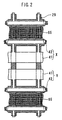
Fig. 2 is a plan view showing the arrangement relationship between the display electrode and the partition. -
Fig. 3 is a plan view showing a partition pattern. -
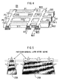
Fig. 4 is a diagram showing a solid structure of the partition. -
Fig. 5 is a schematic diagram showing heat shrink in the partition forming process. -
Fig. 6 is a diagram showing a baking profile in the partition forming process. -
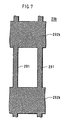
Figs. 7 ,8A and 8B show variations of the partition pattern. -
Figs. 9A-12 show variations of the display electrode pattern. - Hereinafter, the present invention will be explained in detail with reference to embodiments and accompanied drawings.
-
Fig. 1 is a diagram showing a cell structure of a PDP according to the present invention.Fig. 2 is a plan view showing the arrangement relationship between the display electrode and the partition.Fig. 1 is a drawing of an inner structure, which shows a pair of substrate structures being separated from each other. - The
PDP 1 comprises a pair of substrate structures (a structure including a substrate on which cell elements are arranged) 10, 20, and the display surface ES comprises m x n cells. In each cell, the display electrodes X, Y constituting an electrode pair for generating the display discharge are extending in the row direction (the horizontal direction) of the matrix display, and the address electrodes A are extending in the column direction (the vertical direction). - The display electrodes X, Y are arranged on the inner surface of the
glass substrate 11 of thefront substrate structure 10 as a pair for each row. Herein, the "row" means a set of cells whose positions in the column direction are the same, and the number of the cells is equal to the number of columns (m). Each of the display electrodes X and Y includes a transparentconductive film 41 that forms a surface discharge gap (a discharge slit) and a metal film (a bus conductor) 42 that is overlaid on the edge in the column direction. The display electrodes X, Y are covered with adielectric layer 17 having the thickness of approximately 20-40 µm, and the surface of thedielectric layer 17 is coated with aprotection film 18 made of magnesia (MgO). The electrode gap between rows (that is called a reverse slit) is provided with adark color layer 65 that is called a black stripe by applying a paint on the outer surface of theglass substrate 11 or by forming a colored glass layer including fillers such as manganese, iron oxide, chromium and other colorant so as to increase contrast (seeFig. 2 ). - The address electrodes A are arranged on the inner surface of the
glass substrate 21 of theback substrate structure 20 as one for each column and are covered with adielectric layer 24. On thedielectric layer 24, thepartition 29 is disposed, which has a grid pattern with partially low profile structure that is unique to the present invention. Thepartition 29 is made of a baked material of a low melting point glass and includes a portion for dividing the discharge space into columns (hereinafter referred to as a vertical wall) 291 and a portion for dividing a discharge space into rows (hereinafter referred to as a horizontal wall) 292. The intersection of thevertical wall 291 and thehorizontal wall 292 is a common part of them. Thehorizontal wall 292 is lower than thevertical wall 291 by approximately 10 µm. The upper surface of thedielectric layer 24 and the side face of thepartition 29 are covered with red, green and blue colors offluorescent material layers Fig. 1 signify light emission colors of the fluorescent materials. The color arrangement has a repeating pattern of red, green and blue colors in such a way that the cells in a column have the same color. Thefluorescent material layers - As shown in
Fig. 2 , themetal film 42 of each of the display electrodes X, Y is overlaid on thepartition 29 so as to avoid shading and to blind thepartition 29 partially for reducing reflection of external light rays. The transparentconductive film 41 is patterned in such a way that the portion for the surface discharge is substantially separated from the portion overlaid on themetal film 42, for suppressing discharge current so as to enhance the efficiency of light emission. In the case of f 107cm (42 inch) wide VGA type, the portion for the display discharge of the transparentconductive film 41 is separated from thehorizontal wall 292 by a distance more than 30 µm, so that energy loss is largely reduced compared with the case where the distance is less than 30 µm. It is desirable that the distance between thehorizontal wall 292 and the transparentconductive film 41 is set so that the discharge current is reduced by more than 5%. - The
PDP 1 having the above-mentioned structure can be manufactured by the following process. - (1) Providing the
glass substrates substrate structures - (2) Overlaying the
substrate structures - (3) Exhausting the inner air and filling the discharge gas through an air hole that is formed in the
back substrate structure 20. - (4) Closing the air hole.
-
Fig. 3 is a plan view showing a partition pattern.Fig. 4 is a diagram showing a solid structure of the partition. - As shown in
Fig. 3 , the partition pattern is a grid pattern in which each square of the grid pattern encloses a cell C individually. However, it is not a simple check pattern. Namely, the inter-row portion 293 (the portion between the cells aligned in the column direction) of thepartition 29 includes twohorizontal walls 292 and a part of thevertical wall 291. The plan view pattern of theinter-row portion 293 is made a ladder pattern, and aspace 33 is formed between the gas-filledspace 32 that corresponds to each of the cells C aligned in the column direction. Since the dielectric constant of the discharge gas is approximately one eighth of that of a low melting point glass that is a common material of the partition, capacitance between the display electrodes of the neighboring rows is reduced, so that a waste of power consumption can be reduced and response of drive control can be improved. In the check pattern, the side face of thevertical wall 291 and the side face of thehorizontal wall 292 respectively are provided with a fluorescent material, so that the light emission area is enlarged and the light emission efficiency can be improved. - In the
PDP 1 of this embodiment, theinter-row portion 293 of thepartition 29 is made approximately 10 µm lower than other portions, thereby forming an air exhaustion path 90 that has a grid shape in the plan view for enabling air exhaustion both in the column direction and in the row direction. The width W20 of theinter-row portion 293 is substantially large, and the air exhaustion conductance is substantially the same as the stripe pattern. Concrete dimension of thepartition 29 is as follows. - row pitch P1: 1080 µm
- column pitch P2: 360 µm
- width W11 of the upper surface of the vertical wall 291: approximately 70 µm
- width W12 of the bottom surface of the vertical wall 291: approximately 140 µm
- height H1 of the vertical wall 291: approximately 140 µm
- width W21 of the upper surface of the horizontal wall 292: approximately 100 µm
- width W22 of the bottom surface of the horizontal wall 292: approximately 200 µm
- height H2 of the horizontal wall 292: approximately 130 µm
- column direction size D11 of the space 32: approximately 680 µm
- row direction size D22 of the space 32: approximately 290 µm
- column direction size D12 of the space 33: approximately 200 µm
- width W20 of the inter-row portion 293: approximately 400 µm
- It is important that the width W20 of the
inter-row portion 293 is substantially larger than the width W11 of thevertical wall 291, so that the difference between the widths makes a height difference between theinter-row portion 293 and other portions. Namely, in a baking process of a material such as a general low melting point glass having a heat shrink property, as shown schematically inFig. 5 , the shrink quantity in the height direction depends on the width of the pattern. The shrink can be generated both in the width direction and in the height direction as a whole in theportion 29A having a small pattern width. In contrast, in theportion 29B having a large pattern width, the shrink in the width direction is suppressed more at the portion closer to the center in width direction, so that the shrink is generated more in the height direction compensating the suppression in the width direction. Therefore, thethick portion 29B becomes lower than thethin portion 29A. In addition, an isotropic shrink occurs in the upper portion of the wall material layer since the shrink can easily occur in any direction, while the shrink in the direction of the substrate surface is suppressed in the bottom portion due to the bond of the substrate. Therefore, the shrink quantity in the height direction becomes larger than the shrink quantity in the direction of the substrate surface. Namely, even if the width of the upper surface is substantially uniform before baking, and if the widths of the bottom surface are different, the height after baking of the material layer having larger width of the bottom surface becomes lower than the material layer having smaller width of the bottom surface. Considering this fact, the pattern width of the partition is defined as the dimension at the position whose distance from the bottom surface is 10% of the height in this specification. It is desirable that the pattern width of the thick portion is set more than 130% of the pattern width of the thin portion so that a difference of height is generated that is sufficient for air exhaustion. In the case of the above-mentioned partition size, twohorizontal walls 292 and the portion between them (a part of the vertical wall 291) are shrunk in the same way in the height direction, and apartition 29 is obtained that has twointer-row portions 293 having low profile as a whole in theinter-row portion 293 of the ladder pattern. - The composition of the low melting point glass that is a material of the
partition 29 is shown in Table 1.Table 1 Composition of the low melting point glass Components Content (wt%) PbO 50-60 B2O3 5-10 SiO2 10-20 Al2O3 15-25 CaO -5 - Concerning optical characteristics of the
partition 29, it is desirable that it is semitransparent having the absorptance of visual light at approximately 80% per 30 µm of film thickness. If it is semitransparent, light rays generated at the vicinity of the top of the partition pass the partition and contribute to improvement of the luminance, while external rays that entered the partition are reflected by the bottom surface of the partition and are absorbed by the partition before reaching the front surface. Therefore, a display having a good contrast can be realized. - The process of forming the
partition 29 is as follows. - (1) Forming the partition material layer having the thickness of approximately 200 µm made of a uniform paste mixture of a low melting point glass powder having the components shown in Table 1 and a vehicle so as to cover the
dielectric layer 24. The partition material layer may be formed by any method such as a screen printing method, a laminating method in which a green sheet is transferred, or other method. - (2) Drying the partition material layer, and then sticking a photosensitive dry film (or a resist material is applied), and forming a cut mask of the grid pattern corresponding to the
partition 29 by using a photolithography including exposure and development. The mask pattern size is set larger that the desired partition size considering the heat shrink quantity. - (3) Grinding the non-masking portion of the partition material layer by a sandblaster until the
dielectric layer 24 is exposed (the partition material layer is patterned). - (4) Performing heating process according to the baking profile shown in
Fig. 6 to bake the partition material layer so that thepartition 29 is formed. -
Figs. 7 ,8A and 8B show variations of the partition pattern. - The
partition 29b shown inFig. 7 includes avertical wall 291 and ahorizontal wall 292b. Thepartition 29b corresponds to such that theinter-row portion 293 of thepartition 29 shown inFig. 3 is replaced with thehorizontal wall 292b. Thepartition 29c shown inFig. 8A includes avertical wall 291c and ahorizontal wall 292c. The pattern thereof in a plan view is a mesh pattern in which the positions of cells of the neighboring rows are shifted by a half pitch from each other. In thepartition 29c, the pattern width of thehorizontal wall 292c is set larger than the pattern width of thevertical wall 291c, so that thehorizontal wall 292c is lower than thevertical wall 291c, and a mesh-like air exhaustion path 90c is formed. Thepartition 29d shown inFig. 8B includes avertical wall 291d and ahorizontal wall 292d, and the pattern thereof in a plan view is a honeycomb mesh pattern. In thepartition 29d, too, the pattern width of the zigzag bandinghorizontal wall 292d is set larger than the pattern width of thevertical wall 291d, so that thehorizontal wall 292d is lower than thevertical wall 291d, and a mesh-like air exhaustion path 90d is formed. In a PDP having thepartitions vertical walls Fig. 2 , or that three display electrodes are arranged for two rows as a display electrode is shared by two neighboring rows for display. In any way, the entire bus conductor is overlaid on thehorizontal walls -
Figs. 9A-12 show variations of the display electrode pattern. - Each of the display electrodes Xb and Yb shown in
Fig. 9A includes a transparentconductive film 41b and ametal film 42b and corresponds to such display electrodes wherein the pattern of the transparentconductive film 41 of the display electrodes X, Y shown inFig. 2 is changed. In the display electrodes Xb and Yb, the portion of the transparentconductive film 41 to be a discharge surface is connected to the portion that is overlaid on themetal film 42b at the position where it is not overlaid on the vertical wall of thepartition 29. Each of the display electrodes Xc and Yc shown inFig. 9B includes a transparentconductive film 41c and ametal film 42c. Themetal film 42c is arranged at the position where it is not overlaid on the horizontal wall of thepartition 29. In the display electrodes Xd and Yd shown inFig. 10A , the portion of the transparentconductive film 41d that forms the surface discharge gap to be the discharge surface is divided into columns to be a T-shape. The portion of the transparentconductive film 41d that is overlaid on themetal film 42b is straddling over plural columns. Each of the display electrodes Xe and Ye shown inFig. 10B includes a T-shaped transparentconductive film 41e that is divided for each column and ametal film 42b for supplying electricity to the transparent conductive film. The structures ofFigs. 10A and 10B in which the transparent conductive film is divided are effective for suppressing a discharge current and for reducing a capacitance between electrodes. - In the example shown in
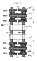
Fig. 11 and in the example shown inFig. 12 , a bus conductor is provided for hiding the reverse slit, so that the process of forming the black stripe can be omitted. InFigs. 11 and12 , thepartition 29e includes avertical wall 291 and ahorizontal wall 292e and corresponds to such partition wherein theinter-row portion 293 of thepartition 29 shown inFig. 3 is replaced with threehorizontal walls 292e. However, the following electrode structure can be applied both to thepartition 29 shown inFig. 2 and to thepartition 29b shown inFig. 7 . - In
Fig. 11 , each of the display electrodes Xf and Yf includes a transparentconductive film 41f and ametal film 42d and is arranged so that the neighboring electrodes of the neighboring rows are the same kind (e.g., in the order of X, Y, Y, X, X, Y, ...). The transparentconductive film 41f is patterned in the same way as the transparentconductive film 41b shown inFig. 9A except for the size of the portion that is overlaid on themetal film 42d. The display electrodes Xf and Yf have a feature in that themetal film 42d as a bus conductor has a large width over two neighboringhorizontal walls 292e. Since an element close to the display surface is drawn at the upper in the figure, a part of themetal film 42d is covered with the transparentconductive film 41f. However, actually in the observation from the display surface side, themetal film 42d can be seen through the transparentconductive film 41f. Namely, theentire metal film 42d works as a shading member for hiding the structure thereunder. Therefore, it is not necessary to provide another shading member (a black stripe) to the inter-row portion (the reverse slit), so that the manufacturing steps of a PDP can be reduced. In addition, since the width of themetal film 42d is enlarged, a line resistance of each of the display electrodes Xf and Yf decreases. Thus, the generation of Joule heat can be reduced, and the voltage drop is also reduced when the discharge current flows. - In
Fig. 12 , each of the display electrodes Xg and Yg includes a transparentconductive film 41g and ametal film 42e and three display electrodes are arranged for two rows so that a display electrode is shared by two neighboring rows for display (in the order of X, Y, X, Y, ...). Themetal film 42e of the display electrodes Xg and Yg have a large width over three neighboringhorizontal walls 292e. The example ofFig. 12 has the same advantage as the example ofFig. 11 in that the manufacturing steps can be reduced, and that the line resistance can be reduced. - In the above-mentioned embodiment, the dimension and the material of the
partition 29 are not limited to the examples. The plan-view pattern of thepartitions - According to the present invention, a PDP that has a good productivity of partition formation and air exhaustion process and can display more brightly and more stably than a PDP that has a stripe-patterned partition can be realized.
- While the presently preferred embodiments of the present invention have been shown and described, it will be understood that the present invention is not limited thereto, and that various changes and modifications may be made by those skilled in the art without departing from the scope of the invention as set forth in the appended claims.
Claims (10)
- A plasma display panel (1) comprising:a pair of substrates (11, 21) arranged so as to define a gap therebetween, each substrate (11,21) having an inner surface bounding said gap;a discharge gas which substantially fills the gap between the substrates (11,21); anda mesh-patterned partition (29; 29b; 29c; 29d; 29e) arranged on the inner surface of one of the substrates (11, 21) and including respective pluralities of vertical walls (29.1; 291c; 291d) and horizontal walls (292; 292b; 292c; 292d; 292e) which divide the gap into a plurality of squares corresponding to an arrangement of discharge cells (C) arranged in respective pluralities of rows and columns;characterized in that:the horizontal walls are wide than the vertical walls,the partition (29; 29b; 29c; 29d; 29e) is composed of a low melting point glass; andthe partition (29; 29b; 29c; 29d; 29e) is formed such that at least a portion of the horizontal wall (292; 292b; 292c; 292d; 292e) which meets a portion of the vertical wall (291; 291 c; 291 d) has a height lower than the height of a remaining portion of the vertical wall (291; 291 c; 291 d), thereby forming an air path (90; 90c; 90d) in the panel.
- The plasma display panel according to claim 1, wherein fluorescent material is arranged on side faces of the vertical wall (291; 291c; 291d) and on side faces of the horizontal walls (292; 292b; 292c; 292d; 292e) in each cell (C) that constitutes a display surface.
- The plasma display panel according to claim 1, wherein the horizontal walls (292; 292b; 292c; 292d; 292e) are of a height lower than that of the vertical walls (291; 291c; 291d).
- The plasma display panel according to claim 1, wherein the partition (29; 29b; 29c; 29d; 29e) includes an inter-row portion (293) between the adjacent rows of the arrangement of the discharge cells (C), the inter-row portion (293) including at least two of the horizontal walls (292), and having a ladder pattern with a plurality of spaces (33) between the horizontal walls (292).
- The plasma display panel according to claim 1, wherein the pair of substrates (11, 21) is provided by a front substrate (11), and a back substrate (21), and wherein the partition (29) is arranged on the back substrate (21), an electrode (X, Y) including a transparent conductive film (41) and a metal film (42) straddling over all the columns is arranged on the front substrate (11), and the metal film (42) and the horizontal walls (292) are overlaid in a plan view.
- The plasma display panel according to claim 1, wherein the vertical walls (291) and the horizontal walls (292) are formed of the same baked material, and the horizontal wall (292) is formed to have a pattern width of 130% or more of the vertical wall (291).
- The plasma display panel according to claim 1, wherein the horizontal wall (292d) has a zigzag pattern such that the partition (29d) has a honeycomb mesh pattern.
- The plasma display panel according to claim 1, wherein the partition (29) includes an inter-row portion (293) between the adjacent rows of the arrangement of the discharge cells (C), the inter-row portion (293) including at least two of the horizontal walls (292), a distance between outer edges of the at least two of the horizontal walls (292) has a width larger than that of the vertical wall (291), and at least portions of the horizontal wall (292) which meet the portions of the vertical walls (291) are formed to be lower than the vertical wall (291) due to heat shrink.
- The plasma display panel according to claim 8, wherein the partition (29) is arranged on the back substrate (21), a display electrode (X, Y) including a transparent electrode (41) and a metal bus electrode (42) straddling over the discharge cells (C) in all the columns is arranged on the front substrate (11), and the metal bus electrode (42) is overlaid on the inter-row portion (293) of the partition (29).
- A method of manufacturing a plasma display panel (1) according to claim 1, the method comprising the steps of:forming a layer made of a partition material of low melting point glass having a heat shrink property on one of the substrates (21), the layer having a constant height;patterning the partition material layer so as to define the mesh-patterned partition (29) including the vertical walls (291) and the horizontal walls (292) thereby to produce a matrix arrangement of a plurality of discharge cells (C) in plural rows and columns that cross each other, each of the horizontal walls (292) having a width larger than that of the vertical walls (291); andbaking the patterned partition material layer in order to form the partition (29) having a portion whose height is reduced in the horizontal wall (292) having the large width.
Applications Claiming Priority (2)
| Application Number | Priority Date | Filing Date | Title |
|---|---|---|---|
| JP2000269569 | 2000-09-06 | ||
| JP2000269569A JP3701185B2 (en) | 2000-09-06 | 2000-09-06 | Method for manufacturing plasma display panel |
Publications (4)
| Publication Number | Publication Date |
|---|---|
| EP1187166A2 EP1187166A2 (en) | 2002-03-13 |
| EP1187166A3 EP1187166A3 (en) | 2004-10-20 |
| EP1187166B1 true EP1187166B1 (en) | 2008-09-03 |
| EP1187166B8 EP1187166B8 (en) | 2008-10-22 |
Family
ID=18756147
Family Applications (1)
| Application Number | Title | Priority Date | Filing Date |
|---|---|---|---|
| EP01301155A Expired - Lifetime EP1187166B8 (en) | 2000-09-06 | 2001-02-09 | Plasma display panel and method for manufacturing the same |
Country Status (7)
| Country | Link |
|---|---|
| US (2) | US6608441B2 (en) |
| EP (1) | EP1187166B8 (en) |
| JP (1) | JP3701185B2 (en) |
| KR (1) | KR100770724B1 (en) |
| CN (2) | CN1311502C (en) |
| DE (1) | DE60135614D1 (en) |
| TW (1) | TW484159B (en) |
Families Citing this family (82)
| Publication number | Priority date | Publication date | Assignee | Title |
|---|---|---|---|---|
| US6586879B1 (en) * | 1999-10-22 | 2003-07-01 | Matsushita Electric Industrial Co., Ltd. | AC plasma display device |
| KR100807942B1 (en) * | 2000-10-10 | 2008-02-28 | 마츠시타 덴끼 산교 가부시키가이샤 | Plasma Display Panel And Method Of Manufacturing The Same |
| KR100399786B1 (en) * | 2001-04-14 | 2003-09-29 | 삼성에스디아이 주식회사 | Plasma Display Panel |
| JP2003132805A (en) * | 2001-08-14 | 2003-05-09 | Sony Corp | Plasma display |
| JP4027194B2 (en) | 2001-10-26 | 2007-12-26 | 三菱電機株式会社 | Plasma display panel substrate, plasma display panel and plasma display apparatus |
| US6793830B2 (en) * | 2002-09-27 | 2004-09-21 | Medtronic, Inc. | Method for forming a microstructure from a monocrystalline substrate |
| KR100484646B1 (en) * | 2002-09-27 | 2005-04-20 | 삼성에스디아이 주식회사 | Plasma display panel |
| JP3910576B2 (en) | 2002-12-17 | 2007-04-25 | 三星エスディアイ株式会社 | Plasma display panel |
| US7323818B2 (en) | 2002-12-27 | 2008-01-29 | Samsung Sdi Co., Ltd. | Plasma display panel |
| EP1435639B1 (en) | 2003-01-02 | 2010-07-28 | Samsung SDI Co., Ltd. | Plasma display panel |
| ATE475983T1 (en) * | 2003-01-02 | 2010-08-15 | Samsung Sdi Co Ltd | PLASMA DISPLAY PANEL |
| JP2004214166A (en) | 2003-01-02 | 2004-07-29 | Samsung Sdi Co Ltd | Plasma display panel |
| CN100416743C (en) * | 2003-01-23 | 2008-09-03 | 友达光电股份有限公司 | Plasma display panel capable of fast air exhausting or ventilating |
| FR2851691A1 (en) * | 2003-02-21 | 2004-08-27 | Thomson Plasma | Plasma display panel comprises discharge cells between two plates and delimited by partitions forming a network, where partitions separating two adjacent cells of the same column have cavities opening at the top of the partitions |
| KR100589331B1 (en) | 2003-02-21 | 2006-06-14 | 삼성에스디아이 주식회사 | Plasma display panel |
| CN100428394C (en) * | 2003-04-18 | 2008-10-22 | 友达光电股份有限公司 | Plasma display with closed discharge groove and its manufacturing method |
| KR100508933B1 (en) * | 2003-07-24 | 2005-08-17 | 삼성에스디아이 주식회사 | Plasma display panel |
| JP4137013B2 (en) | 2003-06-19 | 2008-08-20 | 三星エスディアイ株式会社 | Plasma display panel |
| US7327083B2 (en) * | 2003-06-25 | 2008-02-05 | Samsung Sdi Co., Ltd. | Plasma display panel |
| JP4289040B2 (en) * | 2003-06-26 | 2009-07-01 | 富士ゼロックス株式会社 | Image processing apparatus and method |
| JP2005026011A (en) * | 2003-06-30 | 2005-01-27 | Fujitsu Hitachi Plasma Display Ltd | Plasma display device |
| JP4399196B2 (en) | 2003-07-01 | 2010-01-13 | 日立プラズマディスプレイ株式会社 | Plasma display panel |
| US20050001551A1 (en) * | 2003-07-04 | 2005-01-06 | Woo-Tae Kim | Plasma display panel |
| KR100502919B1 (en) * | 2003-07-11 | 2005-07-21 | 삼성에스디아이 주식회사 | Plasma display panel |
| KR100508949B1 (en) | 2003-09-04 | 2005-08-17 | 삼성에스디아이 주식회사 | Plasma display panel |
| US7425797B2 (en) | 2003-07-04 | 2008-09-16 | Samsung Sdi Co., Ltd. | Plasma display panel having protrusion electrode with indentation and aperture |
| US7208876B2 (en) | 2003-07-22 | 2007-04-24 | Samsung Sdi Co., Ltd. | Plasma display panel |
| KR100578792B1 (en) * | 2003-10-31 | 2006-05-11 | 삼성에스디아이 주식회사 | Plasma Display Panel Suitable for Phosphor Coating |
| KR100589406B1 (en) * | 2003-11-29 | 2006-06-14 | 삼성에스디아이 주식회사 | Plasma display panel |
| KR100589369B1 (en) | 2003-11-29 | 2006-06-14 | 삼성에스디아이 주식회사 | Plasma display panel |
| US20050137017A1 (en) * | 2003-12-09 | 2005-06-23 | Systems In Progress Holding Gmbh | Electronic gaming system |
| WO2005059943A1 (en) * | 2003-12-17 | 2005-06-30 | Hitachi Plasma Patent Licensing Co., Ltd. | Plasma display panel |
| KR100637148B1 (en) * | 2004-02-18 | 2006-10-20 | 삼성에스디아이 주식회사 | Plasma display panel |
| EP1596410A1 (en) * | 2004-03-30 | 2005-11-16 | LG Electronics Inc. | Plasma display panel and manufacture method thereof |
| KR100560480B1 (en) | 2004-04-29 | 2006-03-13 | 삼성에스디아이 주식회사 | Plasma display panel |
| KR100626001B1 (en) * | 2004-05-03 | 2006-09-20 | 삼성에스디아이 주식회사 | Plasma Display Panel And Method Of Manufacturing The Same |
| KR20050112310A (en) * | 2004-05-25 | 2005-11-30 | 삼성에스디아이 주식회사 | Plasma display panel |
| KR100612356B1 (en) * | 2004-05-31 | 2006-08-16 | 삼성에스디아이 주식회사 | Plasma Display Panel with Improved Exhaust Efficiency |
| TW200603046A (en) * | 2004-07-15 | 2006-01-16 | Au Optronics Corp | High contrast plasma display |
| JP2006066148A (en) * | 2004-08-25 | 2006-03-09 | Dainippon Screen Mfg Co Ltd | Panel for planar display device |
| KR100612581B1 (en) * | 2004-11-11 | 2006-08-16 | 엘지전자 주식회사 | Plasma display panel |
| US20060125398A1 (en) * | 2004-11-23 | 2006-06-15 | Lg Electronics Inc. | Plasma display panel |
| KR20060085991A (en) * | 2005-01-25 | 2006-07-31 | 삼성에스디아이 주식회사 | Plasma display panel |
| KR20060087135A (en) * | 2005-01-28 | 2006-08-02 | 삼성에스디아이 주식회사 | Plasma display panel |
| KR100692095B1 (en) * | 2005-02-04 | 2007-03-12 | 엘지전자 주식회사 | Bulkhead of plasma display panel, plasma display panel and manufacturing method thereof |
| US20060175969A1 (en) * | 2005-02-07 | 2006-08-10 | Bae Bum J | Plasma display apparatus, plasma display panel, and manufacturing method of plasma display panel |
| KR100670312B1 (en) * | 2005-03-15 | 2007-01-16 | 삼성에스디아이 주식회사 | Plasma display panel |
| KR100669427B1 (en) * | 2005-03-15 | 2007-01-15 | 삼성에스디아이 주식회사 | Plasma Display Panel And Method Of Manufacturing The Same |
| KR100684791B1 (en) * | 2005-04-08 | 2007-02-20 | 삼성에스디아이 주식회사 | Plasma display panel |
| US20090079323A1 (en) * | 2005-06-02 | 2009-03-26 | Masashi Gotou | Plasma display panel and plasma display panel unit |
| KR100708709B1 (en) * | 2005-08-06 | 2007-04-17 | 삼성에스디아이 주식회사 | Plasma display panel |
| JP2007311129A (en) * | 2006-05-17 | 2007-11-29 | Advanced Pdp Development Corp | Plasma display panel |
| KR100749615B1 (en) * | 2005-09-07 | 2007-08-14 | 삼성에스디아이 주식회사 | Plasma display panel |
| KR100778474B1 (en) * | 2005-09-08 | 2007-11-21 | 엘지전자 주식회사 | Plasma display panel |
| KR100739056B1 (en) * | 2005-11-23 | 2007-07-12 | 삼성에스디아이 주식회사 | Plasma Display Panel And Method Of Manufacturing The Same |
| KR100755306B1 (en) | 2005-12-12 | 2007-09-05 | 엘지전자 주식회사 | Plasma display panel |
| JP2007165090A (en) * | 2005-12-13 | 2007-06-28 | Samsung Sdi Co Ltd | Plasma display panel and manufacturing method thereof |
| KR100761137B1 (en) | 2006-01-05 | 2007-09-21 | 엘지전자 주식회사 | Plasma display panel |
| JP4892987B2 (en) * | 2006-01-23 | 2012-03-07 | パナソニック株式会社 | Plasma display panel |
| JP4792991B2 (en) * | 2006-01-23 | 2011-10-12 | パナソニック株式会社 | Plasma display device |
| WO2007099793A1 (en) * | 2006-02-28 | 2007-09-07 | Toray Industries, Inc. | Member for plasma display and method for producing the same |
| KR20070097191A (en) * | 2006-03-28 | 2007-10-04 | 삼성에스디아이 주식회사 | Plasma display panel |
| KR100730213B1 (en) * | 2006-03-28 | 2007-06-19 | 삼성에스디아이 주식회사 | Plasma display panel |
| KR100768214B1 (en) * | 2006-03-29 | 2007-10-18 | 삼성에스디아이 주식회사 | Plasma display panel |
| US20090160336A1 (en) * | 2006-05-01 | 2009-06-25 | Koji Ohira | Plasma display panel |
| EP1860677B1 (en) * | 2006-05-22 | 2012-12-12 | LG Electronics Inc. | Plasma display apparatus |
| CN101395690A (en) * | 2006-06-07 | 2009-03-25 | 日立等离子显示器股份有限公司 | plasma display panel |
| WO2008001428A1 (en) * | 2006-06-27 | 2008-01-03 | Hitachi Plasma Display Limited | Plasma display panel |
| CN101449351A (en) * | 2006-06-27 | 2009-06-03 | 日立等离子显示器股份有限公司 | Plasma display panel for improving air guided |
| US20090174329A1 (en) * | 2006-07-20 | 2009-07-09 | Hitachi Plasma Display Limited | Plasma display panel |
| WO2008041343A1 (en) * | 2006-09-29 | 2008-04-10 | Hitachi Plasma Display Limited | Plasma display panel and production method thereof |
| JP2008091093A (en) * | 2006-09-29 | 2008-04-17 | Fujitsu Hitachi Plasma Display Ltd | Plasma display panel |
| KR100874070B1 (en) * | 2007-02-21 | 2008-12-12 | 삼성에스디아이 주식회사 | Plasma Display Panel and Manufacturing Method Thereof |
| KR20080095044A (en) * | 2007-04-23 | 2008-10-28 | 삼성에스디아이 주식회사 | Plasma display panel |
| CN101874282A (en) * | 2008-01-07 | 2010-10-27 | Lg电子株式会社 | Plasma display panel having a plurality of discharge cells |
| JP2010170763A (en) * | 2009-01-21 | 2010-08-05 | Panasonic Corp | Plasma display panel |
| JP2010170762A (en) * | 2009-01-21 | 2010-08-05 | Panasonic Corp | Plasma display panel |
| JP2010170759A (en) * | 2009-01-21 | 2010-08-05 | Panasonic Corp | Plasma display panel |
| JP2010170764A (en) * | 2009-01-21 | 2010-08-05 | Panasonic Corp | Plasma display panel |
| JP2010170756A (en) * | 2009-01-21 | 2010-08-05 | Panasonic Corp | Plasma display panel |
| JP2010170760A (en) * | 2009-01-21 | 2010-08-05 | Panasonic Corp | Plasma display panel |
| JP5156710B2 (en) * | 2009-09-17 | 2013-03-06 | パナソニック株式会社 | Plasma display panel |
Family Cites Families (21)
| Publication number | Priority date | Publication date | Assignee | Title |
|---|---|---|---|---|
| FR2260865B1 (en) * | 1974-02-12 | 1976-11-26 | Thomson Csf | |
| US5352478A (en) * | 1982-02-10 | 1994-10-04 | Dai Nippon Insatsu Kabushiki Kaisha | Plasma display panel and method of manufacturing same |
| JPH04206126A (en) | 1990-11-28 | 1992-07-28 | Mitsubishi Electric Corp | Discharge type display device and its manufacture |
| JPH04274141A (en) | 1991-03-01 | 1992-09-30 | Fujitsu Ltd | Plasma display panel |
| JPH04277439A (en) | 1991-03-04 | 1992-10-02 | Dainippon Printing Co Ltd | Plasma display panel and its manufacture |
| JPH0594772A (en) | 1991-10-01 | 1993-04-16 | Nec Corp | Plasma display panel |
| JPH07182978A (en) * | 1993-12-22 | 1995-07-21 | Matsushita Electron Corp | Gas discharge type display apparatus |
| JP3016539B2 (en) * | 1994-09-28 | 2000-03-06 | 株式会社ノリタケカンパニーリミテド | Plasma addressed liquid crystal display |
| JPH09507957A (en) * | 1994-11-04 | 1997-08-12 | オリオン・エレクトリック・カンパニー・リミテッド | Plasma display panel for multi-screen system |
| KR960019415A (en) * | 1994-11-23 | 1996-06-17 | 윤종용 | Plasma display panel |
| JPH08185802A (en) * | 1994-12-28 | 1996-07-16 | Noritake Co Ltd | Discharge display device |
| JPH09115452A (en) | 1995-10-13 | 1997-05-02 | Sumitomo Kinzoku Electro Device:Kk | Barrier structure of plasma display panel |
| JP3015724B2 (en) | 1995-12-28 | 2000-03-06 | 岡谷電機産業株式会社 | Gas discharge display panel and method of manufacturing the same |
| US5909083A (en) * | 1996-02-16 | 1999-06-01 | Dai Nippon Printing Co., Ltd. | Process for producing plasma display panel |
| JPH10308177A (en) * | 1997-05-09 | 1998-11-17 | Hitachi Ltd | Display discharge tube and its driving method |
| TW392186B (en) * | 1997-12-01 | 2000-06-01 | Hitachi Ltd | Plasma display panel and image display using the same |
| JP3705914B2 (en) * | 1998-01-27 | 2005-10-12 | 三菱電機株式会社 | Surface discharge type plasma display panel and manufacturing method thereof |
| JP3116891B2 (en) * | 1998-03-06 | 2000-12-11 | 日本電気株式会社 | Plasma display panel |
| JP3259681B2 (en) | 1998-04-14 | 2002-02-25 | 日本電気株式会社 | AC discharge type plasma display panel and driving method thereof |
| JPH11306993A (en) * | 1998-04-21 | 1999-11-05 | Dainippon Printing Co Ltd | Plasma display panel |
| KR100662073B1 (en) * | 1998-08-28 | 2006-12-27 | 후지쯔 가부시끼가이샤 | Method of forming a rib pattern |
-
2000
- 2000-09-06 JP JP2000269569A patent/JP3701185B2/en not_active Expired - Fee Related
-
2001
- 2001-01-16 KR KR1020010002349A patent/KR100770724B1/en not_active Expired - Fee Related
- 2001-01-31 TW TW090101956A patent/TW484159B/en not_active IP Right Cessation
- 2001-02-08 US US09/778,879 patent/US6608441B2/en not_active Ceased
- 2001-02-09 EP EP01301155A patent/EP1187166B8/en not_active Expired - Lifetime
- 2001-02-09 DE DE60135614T patent/DE60135614D1/en not_active Expired - Fee Related
- 2001-09-06 CN CNB011376058A patent/CN1311502C/en not_active Expired - Fee Related
- 2001-09-06 CN CN2007100854632A patent/CN101013645B/en not_active Expired - Fee Related
-
2005
- 2005-04-25 US US11/113,337 patent/USRE40502E1/en not_active Expired - Fee Related
Also Published As
| Publication number | Publication date |
|---|---|
| US20020047519A1 (en) | 2002-04-25 |
| JP2002083545A (en) | 2002-03-22 |
| CN101013645B (en) | 2012-12-19 |
| US6608441B2 (en) | 2003-08-19 |
| EP1187166B8 (en) | 2008-10-22 |
| CN1311502C (en) | 2007-04-18 |
| KR100770724B1 (en) | 2007-10-29 |
| KR20020020167A (en) | 2002-03-14 |
| CN101013645A (en) | 2007-08-08 |
| CN1344005A (en) | 2002-04-10 |
| TW484159B (en) | 2002-04-21 |
| JP3701185B2 (en) | 2005-09-28 |
| DE60135614D1 (en) | 2008-10-16 |
| USRE40502E1 (en) | 2008-09-16 |
| EP1187166A3 (en) | 2004-10-20 |
| EP1187166A2 (en) | 2002-03-13 |
Similar Documents
| Publication | Publication Date | Title |
|---|---|---|
| EP1187166A2 (en) | Plasma display panel and method for manufacturing the same | |
| EP1763054B1 (en) | Manufacturing method of a plasma display panel | |
| US7102286B2 (en) | Plasma display panel with a dielectric layer having depressions between projections and forming ventilation paths | |
| US6650062B2 (en) | Plasma display panel and method for manufacturing the same | |
| CN100470711C (en) | plasma display panel | |
| US7597604B2 (en) | Method of manufacturing barrier ribs for a plasma display panel | |
| US20050041001A1 (en) | Plasma display panel and manufacturing method | |
| JP4059880B2 (en) | Plasma display panel | |
| KR20050025733A (en) | Plasma display panel and method for manufacturing the same | |
| US7375466B2 (en) | Address electrode design in a plasma display panel | |
| US7646150B2 (en) | Plasma display panel and manufacturing method of the same | |
| EP1180782B1 (en) | Plasma display panel and method of manufacturing the same | |
| US20040007975A1 (en) | Barrier rib structure for plasma display panel | |
| US20070103072A1 (en) | Plasma display panel (PDP) | |
| US20060214584A1 (en) | Plasma display panel | |
| JP4976668B2 (en) | Plasma display panel | |
| JP2010003426A (en) | Plasma display panel and plasma display device | |
| CN101147226A (en) | Discharge type display device | |
| JP2006278134A (en) | Plasma display panel and its manufacturing method | |
| JP2000323041A (en) | Display discharge tube | |
| JP2007165090A (en) | Plasma display panel and manufacturing method thereof | |
| JPH02276134A (en) | Gas electric discharge panel |
Legal Events
| Date | Code | Title | Description |
|---|---|---|---|
| PUAI | Public reference made under article 153(3) epc to a published international application that has entered the european phase |
Free format text: ORIGINAL CODE: 0009012 |
|
| AK | Designated contracting states |
Kind code of ref document: A2 Designated state(s): AT BE CH CY DE DK ES FI FR GB GR IE IT LI LU MC NL PT SE TR |
|
| AX | Request for extension of the european patent |
Free format text: AL;LT;LV;MK;RO;SI |
|
| PUAL | Search report despatched |
Free format text: ORIGINAL CODE: 0009013 |
|
| AK | Designated contracting states |
Kind code of ref document: A3 Designated state(s): AT BE CH CY DE DK ES FI FR GB GR IE IT LI LU MC NL PT SE TR |
|
| AX | Request for extension of the european patent |
Extension state: AL LT LV MK RO SI |
|
| RIC1 | Information provided on ipc code assigned before grant |
Ipc: 7H 01J 9/24 B Ipc: 7H 01J 9/385 B Ipc: 7H 01J 17/49 A |
|
| RIC1 | Information provided on ipc code assigned before grant |
Ipc: 7H 01J 17/16 B Ipc: 7H 01J 9/24 B Ipc: 7H 01J 17/49 A Ipc: 7H 01J 9/385 B |
|
| 17P | Request for examination filed |
Effective date: 20050418 |
|
| AKX | Designation fees paid |
Designated state(s): DE FR GB |
|
| 17Q | First examination report despatched |
Effective date: 20061109 |
|
| GRAP | Despatch of communication of intention to grant a patent |
Free format text: ORIGINAL CODE: EPIDOSNIGR1 |
|
| GRAS | Grant fee paid |
Free format text: ORIGINAL CODE: EPIDOSNIGR3 |
|
| GRAA | (expected) grant |
Free format text: ORIGINAL CODE: 0009210 |
|
| AK | Designated contracting states |
Kind code of ref document: B1 Designated state(s): DE FR GB |
|
| REG | Reference to a national code |
Ref country code: GB Ref legal event code: FG4D |
|
| RAP2 | Party data changed (patent owner data changed or rights of a patent transferred) |
Owner name: HITACHI PLASMA DISPLAY LIMITED |
|
| REF | Corresponds to: |
Ref document number: 60135614 Country of ref document: DE Date of ref document: 20081016 Kind code of ref document: P |
|
| PGFP | Annual fee paid to national office [announced via postgrant information from national office to epo] |
Ref country code: GB Payment date: 20090226 Year of fee payment: 9 |
|
| PLBE | No opposition filed within time limit |
Free format text: ORIGINAL CODE: 0009261 |
|
| STAA | Information on the status of an ep patent application or granted ep patent |
Free format text: STATUS: NO OPPOSITION FILED WITHIN TIME LIMIT |
|
| 26N | No opposition filed |
Effective date: 20090604 |
|
| PGFP | Annual fee paid to national office [announced via postgrant information from national office to epo] |
Ref country code: DE Payment date: 20090424 Year of fee payment: 9 |
|
| PGFP | Annual fee paid to national office [announced via postgrant information from national office to epo] |
Ref country code: FR Payment date: 20100212 Year of fee payment: 10 |
|
| GBPC | Gb: european patent ceased through non-payment of renewal fee |
Effective date: 20100209 |
|
| PG25 | Lapsed in a contracting state [announced via postgrant information from national office to epo] |
Ref country code: DE Free format text: LAPSE BECAUSE OF NON-PAYMENT OF DUE FEES Effective date: 20100901 |
|
| PG25 | Lapsed in a contracting state [announced via postgrant information from national office to epo] |
Ref country code: GB Free format text: LAPSE BECAUSE OF NON-PAYMENT OF DUE FEES Effective date: 20100209 |
|
| REG | Reference to a national code |
Ref country code: FR Ref legal event code: ST Effective date: 20111102 |
|
| PG25 | Lapsed in a contracting state [announced via postgrant information from national office to epo] |
Ref country code: FR Free format text: LAPSE BECAUSE OF NON-PAYMENT OF DUE FEES Effective date: 20110228 |