EP1187091B1 - Method of driving scanning lines of a active matrix liquid crystal device - Google Patents
Method of driving scanning lines of a active matrix liquid crystal device Download PDFInfo
- Publication number
- EP1187091B1 EP1187091B1 EP01307578A EP01307578A EP1187091B1 EP 1187091 B1 EP1187091 B1 EP 1187091B1 EP 01307578 A EP01307578 A EP 01307578A EP 01307578 A EP01307578 A EP 01307578A EP 1187091 B1 EP1187091 B1 EP 1187091B1
- Authority
- EP
- European Patent Office
- Prior art keywords
- gate
- gate lines
- concurrently
- lines
- liquid crystal
- Prior art date
- Legal status (The legal status is an assumption and is not a legal conclusion. Google has not performed a legal analysis and makes no representation as to the accuracy of the status listed.)
- Expired - Lifetime
Links
Images




Classifications
-
- G—PHYSICS
- G09—EDUCATION; CRYPTOGRAPHY; DISPLAY; ADVERTISING; SEALS
- G09G—ARRANGEMENTS OR CIRCUITS FOR CONTROL OF INDICATING DEVICES USING STATIC MEANS TO PRESENT VARIABLE INFORMATION
- G09G3/00—Control arrangements or circuits, of interest only in connection with visual indicators other than cathode-ray tubes
- G09G3/20—Control arrangements or circuits, of interest only in connection with visual indicators other than cathode-ray tubes for presentation of an assembly of a number of characters, e.g. a page, by composing the assembly by combination of individual elements arranged in a matrix no fixed position being assigned to or needed to be assigned to the individual characters or partial characters
- G09G3/34—Control arrangements or circuits, of interest only in connection with visual indicators other than cathode-ray tubes for presentation of an assembly of a number of characters, e.g. a page, by composing the assembly by combination of individual elements arranged in a matrix no fixed position being assigned to or needed to be assigned to the individual characters or partial characters by control of light from an independent source
- G09G3/36—Control arrangements or circuits, of interest only in connection with visual indicators other than cathode-ray tubes for presentation of an assembly of a number of characters, e.g. a page, by composing the assembly by combination of individual elements arranged in a matrix no fixed position being assigned to or needed to be assigned to the individual characters or partial characters by control of light from an independent source using liquid crystals
-
- G—PHYSICS
- G09—EDUCATION; CRYPTOGRAPHY; DISPLAY; ADVERTISING; SEALS
- G09G—ARRANGEMENTS OR CIRCUITS FOR CONTROL OF INDICATING DEVICES USING STATIC MEANS TO PRESENT VARIABLE INFORMATION
- G09G3/00—Control arrangements or circuits, of interest only in connection with visual indicators other than cathode-ray tubes
- G09G3/20—Control arrangements or circuits, of interest only in connection with visual indicators other than cathode-ray tubes for presentation of an assembly of a number of characters, e.g. a page, by composing the assembly by combination of individual elements arranged in a matrix no fixed position being assigned to or needed to be assigned to the individual characters or partial characters
- G09G3/34—Control arrangements or circuits, of interest only in connection with visual indicators other than cathode-ray tubes for presentation of an assembly of a number of characters, e.g. a page, by composing the assembly by combination of individual elements arranged in a matrix no fixed position being assigned to or needed to be assigned to the individual characters or partial characters by control of light from an independent source
- G09G3/36—Control arrangements or circuits, of interest only in connection with visual indicators other than cathode-ray tubes for presentation of an assembly of a number of characters, e.g. a page, by composing the assembly by combination of individual elements arranged in a matrix no fixed position being assigned to or needed to be assigned to the individual characters or partial characters by control of light from an independent source using liquid crystals
- G09G3/3611—Control of matrices with row and column drivers
- G09G3/3648—Control of matrices with row and column drivers using an active matrix
-
- G—PHYSICS
- G09—EDUCATION; CRYPTOGRAPHY; DISPLAY; ADVERTISING; SEALS
- G09G—ARRANGEMENTS OR CIRCUITS FOR CONTROL OF INDICATING DEVICES USING STATIC MEANS TO PRESENT VARIABLE INFORMATION
- G09G2310/00—Command of the display device
- G09G2310/02—Addressing, scanning or driving the display screen or processing steps related thereto
- G09G2310/0202—Addressing of scan or signal lines
- G09G2310/0205—Simultaneous scanning of several lines in flat panels
-
- G—PHYSICS
- G09—EDUCATION; CRYPTOGRAPHY; DISPLAY; ADVERTISING; SEALS
- G09G—ARRANGEMENTS OR CIRCUITS FOR CONTROL OF INDICATING DEVICES USING STATIC MEANS TO PRESENT VARIABLE INFORMATION
- G09G2320/00—Control of display operating conditions
- G09G2320/02—Improving the quality of display appearance
- G09G2320/0219—Reducing feedthrough effects in active matrix panels, i.e. voltage changes on the scan electrode influencing the pixel voltage due to capacitive coupling
-
- G—PHYSICS
- G09—EDUCATION; CRYPTOGRAPHY; DISPLAY; ADVERTISING; SEALS
- G09G—ARRANGEMENTS OR CIRCUITS FOR CONTROL OF INDICATING DEVICES USING STATIC MEANS TO PRESENT VARIABLE INFORMATION
- G09G2320/00—Control of display operating conditions
- G09G2320/02—Improving the quality of display appearance
- G09G2320/0223—Compensation for problems related to R-C delay and attenuation in electrodes of matrix panels, e.g. in gate electrodes or on-substrate video signal electrodes
-
- G—PHYSICS
- G09—EDUCATION; CRYPTOGRAPHY; DISPLAY; ADVERTISING; SEALS
- G09G—ARRANGEMENTS OR CIRCUITS FOR CONTROL OF INDICATING DEVICES USING STATIC MEANS TO PRESENT VARIABLE INFORMATION
- G09G3/00—Control arrangements or circuits, of interest only in connection with visual indicators other than cathode-ray tubes
- G09G3/20—Control arrangements or circuits, of interest only in connection with visual indicators other than cathode-ray tubes for presentation of an assembly of a number of characters, e.g. a page, by composing the assembly by combination of individual elements arranged in a matrix no fixed position being assigned to or needed to be assigned to the individual characters or partial characters
- G09G3/34—Control arrangements or circuits, of interest only in connection with visual indicators other than cathode-ray tubes for presentation of an assembly of a number of characters, e.g. a page, by composing the assembly by combination of individual elements arranged in a matrix no fixed position being assigned to or needed to be assigned to the individual characters or partial characters by control of light from an independent source
- G09G3/36—Control arrangements or circuits, of interest only in connection with visual indicators other than cathode-ray tubes for presentation of an assembly of a number of characters, e.g. a page, by composing the assembly by combination of individual elements arranged in a matrix no fixed position being assigned to or needed to be assigned to the individual characters or partial characters by control of light from an independent source using liquid crystals
- G09G3/3611—Control of matrices with row and column drivers
- G09G3/3614—Control of polarity reversal in general
Definitions
- the present invention relates to the driving technology of liquid crystal devices and more particularly liquid crystal displays (LCD).
- Embodiments relate to a method of driving a gate line in a large sized and high resolution LCD which enables extension of a line time by making a falling time of scan signals different while concurrently driving plural gate lines.
- liquid crystal devices utilize the optical property of liquid crystal in which a molecular arrangement of the liquid crystal is varied when an electric field is applied to the liquid crystal.
- Different applications of liquid crystal devices include beam steering devices, light modulators and displays used for displaying characters, symbols, or graphics.
- the LCD is one kind of flat panel display in which liquid crystal technologies are combined with semiconductor technologies.
- Thin film transistor (TFT) LCDs have thin film transistors as the switching element for turning on and off pixels. As the TFTs are turned on or off, the pixels are turned on or off.
- a general TFT LCD includes a plurality of cells arranged in a matrix configuration.
- a unit cell includes a TFT 132 serving as the switching element, a liquid crystal cell 134 and a storage capacitor C STG .
- Sources of the TFTs are connected to data lines (D1-DN) arranged in a column direction and the data lines are connected to a source driver 120.
- Gates of the TFTs are connected to gate lines (G1-GM) arranged in a row direction and the gate lines are connected to a gate driver 110, thereby enabling a display having an PxQ resolution.
- SVGA level has a resolution of 800x600
- XGA level has a resolution of 1024x768
- UXGA level has a resolution of 1,600x1200.
- the source driver 120 may also be referred to as a data driver or column driver and the gate driver as a scan driver or row driver.
- the liquid crystal cell 134 is connected to the drain of the TFT 132 at a pixel electrode and is disposed between the pixel electrode and a common electrode of an upper panel.
- the pixel electrode is made of a transparent conductive material such as indium tin oxide (ITO).
- ITO indium tin oxide
- the common electrode may also be made of a transparent conductive material such as ITO and applies a common voltage VCOM to the liquid crystal cells.
- the storage capacitor C STG maintains a voltage applied to the pixel electrode during a constant time and controls light transmittance by varying an orientation state of liquid crystal molecules in the liquid crystal cell.
- One end of the storage C STG can be connected to an independent electrode or gate electrode, which is called "storage on gate" mode.
- inversion driving methods i.e., a field inversion driving method which changes the voltage polarity of all pixels every field at once, a line inversion driving method which changes the voltage polarity of every pixel connected to a single scan line, a column inversion driving method which changes the voltage polarity of a column every field and a dot inversion which changes the polarity of pixel units.
- a field inversion driving method which changes the voltage polarity of all pixels every field at once
- line inversion driving method which changes the voltage polarity of every pixel connected to a single scan line
- column inversion driving method which changes the voltage polarity of a column every field
- a dot inversion which changes the polarity of pixel units.
- the voltage, which is applied to the pixel electrode through the drain electrode of the TFT is alternately changed such that it has a positive (+) or negative (-) direction with respect to the common voltage VCOM.
- Fig. 2 is a schematic view showing a general gate driver.
- a gate driver 110 includes a shift register 111, a level shifter 112 and output buffers 113.
- the shift register 111 receives a vertical synchronous signal and a vertical clock signal, and thereby generates scan pulses sequentially.
- the level shifter 112 shifts a voltage level of the scan pulses to approximately 30 V.
- the output buffers 113 provide respective gate lines of G1-GM with the level-shifted scan pulses.
- the most general driving method that is used to drive gates is the progressive scanning method as shown in Fig. 3 . Since the progressive scanning method scans only a single gate line (or scan line) during one line time (1H), respective gate driving signals are sequentially applied to gate lines every 1H.
- Fig. 4 shows driving signals used in the conventional interlace scanning method in order to increase the line time.
- the conventional interlace scanning method has a line time twice as long as the progressive scanning method.
- the interlace scanning method has a drawback in that the vertical resolution decreases by half since the same video signal is transmitted into pixels connected to two gate lines. Accordingly, these conventional gate-driving methods are not alternative methods when considering the current trend for high resolution.
- JP 07056143 discloses an image display apparatus that includes a field sequential liquid crystal display (FSLCD) that employs red, green and blue LEDs.
- the scanning circuit is provided for supplying a scanning signal to each of the pixels, however, this document does not disclose extending the turn-on time of a scan signal compared with a progressive scanning method.
- US 5,568,163 discloses an apparatus for driving a gate storage type liquid crystal display panel having gate lines.
- two gate pulse signals are simultaneously supplied to two adjacent gate lines to drive them.
- the two gate pulses differ in that at least one of a rising edge and a falling edge are one of the two gate pulses differs from that of the other.
- EP 479552 discloses a liquid crystal display apparatus in which a selection signal is simultaneously applied to two scanning signals. The application of the selection signal to one of the two scanning signal lines is terminated earlier than that of the selection signal to the other one of the two scanning signal lines.
- US 5,648,793 discloses a driving system for a matrix liquid crystal display in which the picture elements in adjacent rows and/or adjacent column are applied with signals of opposite pluralities. These pluralities are reversed for every other field of a picture frame.
- the present invention is directed to a method for driving gates of an LCD that substantially obviates one or more problems due to limitations and disadvantages of the related art.
- An aim of embodiments of the present invention is to provide a method for driving gates of an LCD enabling to extend the line without lowering the resolution by rendering a falling time of scan signals different while driving plural gate lines at the same time.
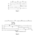
- Fig.5 shows waveforms of gate driving signals in a line time extending driving method to scan two gate lines concurrently in accordance with the present invention.
- gate driving signals applied to two gate lines rise concurrently but fall at different timings.
- the conventional two gate lines driving method if gate driving signals are concurrently applied to gate lines G1 and G2, identical image signals are applied to pixels sharing the same data line.
- the gate line driving method of the present invention since the first gate driving signal G1 falls first, an image signal corresponding to pixels connected to the first gate line is sampled. After that, the second gate driving signal G2 falls and thereby an image signal corresponding to pixels connected to the second gate line is sampled.
- the gate driving method of the present invention it becomes possible to extend the line time 30-70% longer than that in the normal progressive scanning method and at the same time it becomes possible to transmit image signals corresponding to pixels connected to each of the gate lines unlike the conventional interlace scanning method in which two gate lines are concurrently driven and they concurrently fall.
- a specific extending percentage of the line time may be different depending on a panel characteristic.
- the conventional progressive scanning method when driving gate lines of an LCD panel having a resolution of XGA level (1024x768) using a frame frequency of 75 Hz, the conventional progressive scanning method has a line time of approximately 17 ⁇ sec but a line time extending driving method of the present invention can have a line time of approximately 22-30 ⁇ sec.
- the line time extending driving method of the present invention is executed by concurrently driving a chosen number N of gate lines.
- Fig. 5 corresponds to a method of concurrently selecting two gate lines
- Fig. 6 corresponds to a method of concurrently selecting three gate lines
- Fig. 7 corresponds to a method of concurrently selecting four gate lines.
- the line time extending driving method of the present invention performs an N-line inversion driving in which image signals having the same polarity are transferred to pixels connected gate lines which are concurrently selected.
- N-line inversion driving such an inversion is performed every line in the column direction and is performed every two lines in the row direction.
- Pixels of a TFT-LCD can be modeled in a circuit diagram of Fig. 9 .
- symbols D1 and D2 are data lines
- G1 and G2 are gate lines
- C LC is a liquid crystal cell modeled as a capacitor
- C STG is a storage capacitance, respectively.
- Symbols C GS1 and C GS2 indicate parasitic capacitances.
- a voltage of the liquid crystal cell C LC is coupled through the parasitic capacitance C GS1 and thereby the voltage is varied.
- a voltage variation amount is also generated by the parasitic capacitance C GS2 .
- a voltage of the liquid crystal is coupled with the parasitic capacitance C GS2 and thereby the voltage is varied.
- the pixels connected to an odd gate line generate only a voltage variation amount of ⁇ V P1 defined by the equation 1 while the pixels connected to an even gate line generate a voltage variation amount corresponding to a sum of ⁇ V P1 and ⁇ V ⁇ V P2 defined by equation 2.
- ⁇ ⁇ V P ⁇ 2 C GS ⁇ 1 C LC + C STG + C GS ⁇ 1 + C GS ⁇ 2 ⁇ - V G + C GS ⁇ 2 C LC + C STG + C GS ⁇ 1 + C GS ⁇ 2 ⁇ V G
- the pixels connected to the odd gate lines have a different voltage variation to that of the pixels connected to the even gate lines. This is because when the image signal is sampled to the pixels connected to the gate line of G1, only a gate driving signal applied to the gate line of G1 falls while when the image signal is sampled to the pixels connected to the gate line of G2, falling of a gate driving signal applied to the gate line of G2 and rising of a gate driving signal applied to the gate line of G3 are concurrently generated. As a result, a voltage difference ⁇ Vp between even gate lines and odd gate lines is generated and thereby the picture quality may be lowered.
- another embodiment of the present invention partially modifies the gate driving method of the present invention provided previously.
- the present embodiment since the voltage difference ⁇ Vp between pixels connected to even gate lines and odd gate lines is due to a difference between the gate driving signals applied to the even gate lines and the odd gate lines, the present embodiment renders the odd gate lines and the even gate lines to be under the same driving condition.
- the driving method of the present invention shows and describes embodiments in which the gate driving signals applied to the gate lines rise concurrently and fall at different timings, it is not limited to the above-described embodiments.
- the present invention makes it possible to extend a line time without lowering of the resolution by allowing the gate driving signals to fall concurrently and then to rise at different timings depending on characteristics of the used LCD panel, thus driving plural gate lines concurrently while transferring video signals to the gate lines at different rising timings.
- the gate driving signal applied to the odd gate line may have the same falling condition as the gate signal applied to the even gate line, thereby preventing degradation in picture quality.
Landscapes
- Engineering & Computer Science (AREA)
- Chemical & Material Sciences (AREA)
- Crystallography & Structural Chemistry (AREA)
- Physics & Mathematics (AREA)
- Computer Hardware Design (AREA)
- General Physics & Mathematics (AREA)
- Theoretical Computer Science (AREA)
- Liquid Crystal Display Device Control (AREA)
- Liquid Crystal (AREA)
- Control Of Indicators Other Than Cathode Ray Tubes (AREA)
Abstract
Description
- The present invention relates to the driving technology of liquid crystal devices and more particularly liquid crystal displays (LCD). Embodiments relate to a method of driving a gate line in a large sized and high resolution LCD which enables extension of a line time by making a falling time of scan signals different while concurrently driving plural gate lines.
- Generally, liquid crystal devices utilize the optical property of liquid crystal in which a molecular arrangement of the liquid crystal is varied when an electric field is applied to the liquid crystal. Different applications of liquid crystal devices include beam steering devices, light modulators and displays used for displaying characters, symbols, or graphics. The LCD is one kind of flat panel display in which liquid crystal technologies are combined with semiconductor technologies.
- Thin film transistor (TFT) LCDs have thin film transistors as the switching element for turning on and off pixels. As the TFTs are turned on or off, the pixels are turned on or off.
- As shown in
Fig. 1 , a general TFT LCD includes a plurality of cells arranged in a matrix configuration. A unit cell includes aTFT 132 serving as the switching element, aliquid crystal cell 134 and a storage capacitor CSTG. Sources of the TFTs are connected to data lines (D1-DN) arranged in a column direction and the data lines are connected to asource driver 120. Gates of the TFTs are connected to gate lines (G1-GM) arranged in a row direction and the gate lines are connected to agate driver 110, thereby enabling a display having an PxQ resolution. For instance, SVGA level has a resolution of 800x600, XGA level has a resolution of 1024x768 and UXGA level has a resolution of 1,600x1200. - The
source driver 120 may also be referred to as a data driver or column driver and the gate driver as a scan driver or row driver. - Referring to
Fig. 1 , theliquid crystal cell 134 is connected to the drain of theTFT 132 at a pixel electrode and is disposed between the pixel electrode and a common electrode of an upper panel. The pixel electrode is made of a transparent conductive material such as indium tin oxide (ITO). When a turn on signal is applied to gate of theTFT 132, the pixel electrode transfers a signal voltage applied through thesource driver 120 to theliquid crystal cell 134. The common electrode may also be made of a transparent conductive material such as ITO and applies a common voltage VCOM to the liquid crystal cells. The storage capacitor CSTG maintains a voltage applied to the pixel electrode during a constant time and controls light transmittance by varying an orientation state of liquid crystal molecules in the liquid crystal cell. One end of the storage CSTG can be connected to an independent electrode or gate electrode, which is called "storage on gate" mode. - In driving this pixel array, if a driving voltage is applied to the liquid crystal only in one direction, degradation of the liquid crystal is accelerated. To avoid this, there is used an inversion which periodically applies an image data voltage applied to the liquid crystal in an opposite polarity. The period of such an inversion is normally one field.
- There are four inversion driving methods, i.e., a field inversion driving method which changes the voltage polarity of all pixels every field at once, a line inversion driving method which changes the voltage polarity of every pixel connected to a single scan line, a column inversion driving method which changes the voltage polarity of a column every field and a dot inversion which changes the polarity of pixel units. In any case, the voltage, which is applied to the pixel electrode through the drain electrode of the TFT is alternately changed such that it has a positive (+) or negative (-) direction with respect to the common voltage VCOM.
-
Fig. 2 is a schematic view showing a general gate driver. Referring toFig. 2 , agate driver 110 includes ashift register 111, alevel shifter 112 andoutput buffers 113. Theshift register 111 receives a vertical synchronous signal and a vertical clock signal, and thereby generates scan pulses sequentially. Thelevel shifter 112 shifts a voltage level of the scan pulses to approximately 30 V. Theoutput buffers 113 provide respective gate lines of G1-GM with the level-shifted scan pulses. - Here, the most general driving method that is used to drive gates is the progressive scanning method as shown in
Fig. 3 . Since the progressive scanning method scans only a single gate line (or scan line) during one line time (1H), respective gate driving signals are sequentially applied to gate lines every 1H. - On the other hand, as liquid crystal devices increase in size, the resistance of data lines and the load of capacitance increase. Thus in a display the time for which the data driving circuit transmits a video signal to the pixel is more and more shortened. This may lead to insufficient charge of the pixel and lowers image quality. Therefore, this problem should be necessarily resolved.
-
Fig. 4 shows driving signals used in the conventional interlace scanning method in order to increase the line time. Referring toFig. 4 , the conventional interlace scanning method has a line time twice as long as the progressive scanning method. - However, the interlace scanning method has a drawback in that the vertical resolution decreases by half since the same video signal is transmitted into pixels connected to two gate lines. Accordingly, these conventional gate-driving methods are not alternative methods when considering the current trend for high resolution.
-
JP 07056143 -
US 5,568,163 discloses an apparatus for driving a gate storage type liquid crystal display panel having gate lines. In the disclosed apparatus two gate pulse signals are simultaneously supplied to two adjacent gate lines to drive them. The two gate pulses differ in that at least one of a rising edge and a falling edge are one of the two gate pulses differs from that of the other. -
EP 479552 -
US 5,648,793 discloses a driving system for a matrix liquid crystal display in which the picture elements in adjacent rows and/or adjacent column are applied with signals of opposite pluralities. These pluralities are reversed for every other field of a picture frame. - Accordingly, the present invention is directed to a method for driving gates of an LCD that substantially obviates one or more problems due to limitations and disadvantages of the related art.
- An aim of embodiments of the present invention is to provide a method for driving gates of an LCD enabling to extend the line without lowering the resolution by rendering a falling time of scan signals different while driving plural gate lines at the same time.
- According to one aspect of the invention there is provided a method for driving gates of an LCD as set out in
Claim 1. Preferred features of this aspect are set out inClaims 2 to 4. - Additional advantages, objects, and features of the invention will be set forth in part in the description which follows and in part will become apparent to those having ordinary skill in the art upon examination of the following or may be learned from practice of the invention. The objectives and other advantages of the invention may be realized and attained by the structure particularly pointed out in the written description and claims hereof as well as the appended drawings.
- The accompanying drawings, which are included to provide a further understanding of the invention and are incorporated in and constitute a part of this application, illustrate embodiment(s) of the invention and together with the description serve to explain the principle of the invention. In the drawings:
-
Fig.1 is an equivalent circuit diagram of a general TFT-LCD; -
Fig.2 is a schematic view of a general gate driving circuit; -
Fig.3 shows waveforms of gate driving signals of a general progressive scanning method; -
Fig.4 shows waveforms of gate driving signals of an interlace scanning method so as to increase the line time; -
Fig. 5 shows waveforms of gate driving signals of a line time extending driving method to scan two gate lines concurrently in accordance with an embodiment of the present invention; -
Fig. 6 shows waveforms of gate driving signals of a line time extending driving method to scan three gate lines concurrently in accordance with an embodiment of the present invention; -
Fig. 7 shows waveforms of gate driving signals of a line time extending driving method to scan four gate lines concurrently in accordance with an embodiment of the present invention; -
Fig. 8 is a table showing a line polarity of N-th and (N+1)-th when inversion-driving two gate lines in accordance with the embodiment ofFig. 5 ; -
Fig. 9 is a general circuit diagram of a TFT-LCD pixel useful in understanding the present invention; and -
Fig. 10 shows waveforms of gate driving signals of a line time extending driving method to scan two gate lines concurrently in accordance with an embodiment of the present invention. - Referring now to the first embodiment,
Fig.5 shows waveforms of gate driving signals in a line time extending driving method to scan two gate lines concurrently in accordance with the present invention. - Referring to
Fig. 5 , in this embodiment gate driving signals applied to two gate lines rise concurrently but fall at different timings. In the conventional two gate lines driving method, if gate driving signals are concurrently applied to gate lines G1 and G2, identical image signals are applied to pixels sharing the same data line. By contrast, in the gate line driving method of the present invention, since the first gate driving signal G1 falls first, an image signal corresponding to pixels connected to the first gate line is sampled. After that, the second gate driving signal G2 falls and thereby an image signal corresponding to pixels connected to the second gate line is sampled. - Using the gate driving method of the present invention, it becomes possible to extend the line time 30-70% longer than that in the normal progressive scanning method and at the same time it becomes possible to transmit image signals corresponding to pixels connected to each of the gate lines unlike the conventional interlace scanning method in which two gate lines are concurrently driven and they concurrently fall. Here, a specific extending percentage of the line time may be different depending on a panel characteristic.
- For example, when driving gate lines of an LCD panel having a resolution of XGA level (1024x768) using a frame frequency of 75 Hz, the conventional progressive scanning method has a line time of approximately 17 µsec but a line time extending driving method of the present invention can have a line time of approximately 22-30 µsec.
- The line time extending driving method of the present invention is executed by concurrently driving a chosen number N of gate lines. For instance,
Fig. 5 corresponds to a method of concurrently selecting two gate lines,Fig. 6 corresponds to a method of concurrently selecting three gate lines andFig. 7 corresponds to a method of concurrently selecting four gate lines. - Thus, as the number of lines which can be concurrently selected and then driven increases, it is possible to secure longer line times and to extend the number of selectable lines. And, as shown in
Fig. 5 ,6 and 7 , the line time extending driving method of the present invention performs an N-line inversion driving in which image signals having the same polarity are transferred to pixels connected gate lines which are concurrently selected. In other words, as shown inFig. 8 of describing one example of two lines inversion driving, such an inversion is performed every line in the column direction and is performed every two lines in the row direction. When driving N lines concurrently, such an inversion is performed every N lines. - In the meanwhile, according to the gate line driving method of the present invention in which the falling timings of two gate lines are different from each other while the two gate lines are concurrently driven, it is possible to anticipate an extension of the line time but there may be occur a voltage difference of ΔVp between pixels in even gate lines and odd gate lines. This voltage difference will now be explained.
- Pixels of a TFT-LCD can be modeled in a circuit diagram of
Fig. 9 . InFig. 9 , symbols D1 and D2 are data lines, G1 and G2 are gate lines, CLC is a liquid crystal cell modeled as a capacitor and CSTG is a storage capacitance, respectively. Symbols CGS1 and CGS2 indicate parasitic capacitances. - Referring to
Fig. 9 , as a gate driving signal of G1 falls, a voltage of the liquid crystal cell CLC is coupled through the parasitic capacitance CGS1 and thereby the voltage is varied. A variation amount in this voltage ΔVP1 can be obtained from equation 1:-
where CLC is a capacitance of the liquid crystal and VG is a magnitude in the gate driving signal. - A voltage variation amount is also generated by the parasitic capacitance CGS2. In other words, as a gate signal of G2 rises, a voltage of the liquid crystal is coupled with the parasitic capacitance CGS2 and thereby the voltage is varied.
- As shown in
Fig. 9 , the pixels connected to an odd gate line generate only a voltage variation amount of ΔVP1 defined by theequation 1 while the pixels connected to an even gate line generate a voltage variation amount corresponding to a sum of ΔVP1 and ΔV ΔVP2 defined byequation 2.
- Thus, the pixels connected to the odd gate lines have a different voltage variation to that of the pixels connected to the even gate lines. This is because when the image signal is sampled to the pixels connected to the gate line of G1, only a gate driving signal applied to the gate line of G1 falls while when the image signal is sampled to the pixels connected to the gate line of G2, falling of a gate driving signal applied to the gate line of G2 and rising of a gate driving signal applied to the gate line of G3 are concurrently generated. As a result, a voltage difference ΔVp between even gate lines and odd gate lines is generated and thereby the picture quality may be lowered.
- In order to resolve the aforementioned drawbacks, as shown in
Fig. 10 , another embodiment of the present invention partially modifies the gate driving method of the present invention provided previously. In other words, as aforementioned, since the voltage difference ΔVp between pixels connected to even gate lines and odd gate lines is due to a difference between the gate driving signals applied to the even gate lines and the odd gate lines, the present embodiment renders the odd gate lines and the even gate lines to be under the same driving condition. - For instance, when driving two gate lines as shown in
Fig. 10 , gate driving signals which are applied to even gate lines of G2, G4 and so on fall before gate driving signals which are applied to odd gate lines of G1, G3 and so on fall, and the gate driving signals applied to even gate lines of G2, G4 and so on again rise when the gate driving signals which are being applied to odd gate lines of G1, G3 and so on fall. As a result, all of the pixels connected to the even and odd gate lines have an identical condition for generation of the voltage difference ΔVp and thus the voltage difference problem between the pixels connected to the even and odd gate lines can be resolved. - While the driving method of the present invention shows and describes embodiments in which the gate driving signals applied to the gate lines rise concurrently and fall at different timings, it is not limited to the above-described embodiments. In other words, the present invention makes it possible to extend a line time without lowering of the resolution by allowing the gate driving signals to fall concurrently and then to rise at different timings depending on characteristics of the used LCD panel, thus driving plural gate lines concurrently while transferring video signals to the gate lines at different rising timings.
- As described above, using embodiments of a gate line driving method of the present invention, it becomes possible to increase a line time without lowering the resolution and possible to sufficiently charge/discharge the pixel electrode by making different a falling time of scan signals while concurrently driving plural gate lines.
- Further, the gate driving signal applied to the odd gate line may have the same falling condition as the gate signal applied to the even gate line, thereby preventing degradation in picture quality.
- The foregoing embodiments are merely exemplary and are not to be construed as limiting the present invention. The present teachings can be readily applied to other types of apparatus, especially other apparatus using liquid crystals. The description of the present invention is intended to be illustrative, and not to limit the scope of the claims. Many alternatives, modifications, and variations will be apparent to those skilled in the art.
Claims (4)
- A method of driving gate lines of a liquid crystal display including a plurality of pixels that respectively are comprised of one TFT, a liquid crystal cell and a storage capacitor, the pixels being coupled to a plurality of gate lines sand a plurality of data lines comprising:to select concurrently a group of N consecutive gate lines, N being at least equal to 2, and to apply to each of gate lines belonging to the group a different gate signal wherein all the gate signals applied to the group are concurrently transitioned in a first direction and are successively transitioned in a second direction in order at different times after a time T1 which corresponds to the time necessary to scan a gate line in a conventional progressive scanning method has elapsed and up to and including a time TN which corresponds to the time necessary to scan N gate lines in the same conventional progressive scanning method has elapsed;to sample successively the different data signals present on the data lines corresponding to the pixels of each gate line at the different transitions in the second direction of the scan pulses applied to each gate line of the group; andto perform a N-gate line polarity inversion such that all the data signals transferred to the pixels connected to the same group of concurrently selected N gate lines have the same polarity.
- A method according to claim 1, wherein the transition in the first direction corresponds to a rising edge and the transition in the second direction corresponds to a falling edge.
- A method according to claim 2, wherein all the gate signals applied to the group of the N consecutive gate lines rise concurrently, the gate lines greater than N fall before the Nth gate line falls, and the gate lines greater than N rise concurrently when the Nth gate line falls.
- A method according to claim 1, wherein the transition in the first direction corresponds to a falling edge and the transition in the second direction corresponds to a rising edge.
Applications Claiming Priority (2)
| Application Number | Priority Date | Filing Date | Title |
|---|---|---|---|
| KR1020000053555A KR100350726B1 (en) | 2000-09-08 | 2000-09-08 | Method Of Driving Gates of LCD |
| KR2000053555 | 2000-09-08 |
Publications (3)
| Publication Number | Publication Date |
|---|---|
| EP1187091A2 EP1187091A2 (en) | 2002-03-13 |
| EP1187091A3 EP1187091A3 (en) | 2004-05-12 |
| EP1187091B1 true EP1187091B1 (en) | 2008-05-28 |
Family
ID=19688298
Family Applications (1)
| Application Number | Title | Priority Date | Filing Date |
|---|---|---|---|
| EP01307578A Expired - Lifetime EP1187091B1 (en) | 2000-09-08 | 2001-09-06 | Method of driving scanning lines of a active matrix liquid crystal device |
Country Status (7)
| Country | Link |
|---|---|
| US (2) | US7068249B2 (en) |
| EP (1) | EP1187091B1 (en) |
| JP (1) | JP4776830B2 (en) |
| KR (1) | KR100350726B1 (en) |
| CN (1) | CN1249505C (en) |
| AT (1) | ATE397264T1 (en) |
| DE (1) | DE60134198D1 (en) |
Families Citing this family (19)
| Publication number | Priority date | Publication date | Assignee | Title |
|---|---|---|---|---|
| KR100350726B1 (en) * | 2000-09-08 | 2002-08-30 | 권오경 | Method Of Driving Gates of LCD |
| KR100552905B1 (en) * | 2003-06-30 | 2006-02-22 | 엘지.필립스 엘시디 주식회사 | Driving device and driving method of liquid crystal display |
| KR100621864B1 (en) * | 2003-11-18 | 2006-09-13 | 엘지.필립스 엘시디 주식회사 | Driving Method of LCD |
| KR20050071957A (en) * | 2004-01-05 | 2005-07-08 | 삼성전자주식회사 | Liquid crystal display device and method for driving the same |
| KR100688498B1 (en) * | 2004-07-01 | 2007-03-02 | 삼성전자주식회사 | Liquid crystal panel with integrated gate driver and its driving method |
| KR101234422B1 (en) * | 2006-05-11 | 2013-02-18 | 엘지디스플레이 주식회사 | Liquid crystal display and method driving for the same |
| CN101256758B (en) * | 2008-04-11 | 2010-08-18 | 友达光电股份有限公司 | Driving method of liquid crystal display panel and liquid crystal display thereof |
| KR101469028B1 (en) | 2008-08-11 | 2014-12-04 | 삼성디스플레이 주식회사 | Display device |
| US8432413B2 (en) * | 2008-11-17 | 2013-04-30 | Xrfiles, Inc. | System and method for the display of extended bit depth high resolution images |
| CN102576517B (en) * | 2009-10-16 | 2014-11-19 | 夏普株式会社 | Display driving circuit, display device and display driving method |
| JP5724243B2 (en) * | 2010-08-19 | 2015-05-27 | セイコーエプソン株式会社 | Liquid crystal drive device, liquid crystal display device, electronic apparatus, and liquid crystal drive method |
| KR101832950B1 (en) | 2011-03-28 | 2018-04-16 | 삼성디스플레이 주식회사 | Display device |
| KR101969952B1 (en) | 2012-06-05 | 2019-04-18 | 삼성디스플레이 주식회사 | Display device |
| KR101989150B1 (en) * | 2012-10-05 | 2019-10-01 | 삼성디스플레이 주식회사 | Display panel and display apparatus having the same |
| JP6467952B2 (en) * | 2014-04-04 | 2019-02-13 | セイコーエプソン株式会社 | Driver, electro-optical device and electronic apparatus |
| US10403224B2 (en) * | 2016-08-10 | 2019-09-03 | Novatek Microelectronics Corp. | Control method and control device for charging time sharing |
| CN106409252A (en) * | 2016-09-22 | 2017-02-15 | 京东方科技集团股份有限公司 | Array substrate and driving method thereof, display panel and display device |
| CN114187859B (en) * | 2020-09-14 | 2024-03-15 | 京东方科技集团股份有限公司 | Display driving method and display device |
| CN114114766B (en) | 2021-11-30 | 2022-09-27 | Tcl华星光电技术有限公司 | Liquid crystal display panel, driving method thereof and display device |
Family Cites Families (12)
| Publication number | Priority date | Publication date | Assignee | Title |
|---|---|---|---|---|
| US5206634A (en) * | 1990-10-01 | 1993-04-27 | Sharp Kabushiki Kaisha | Liquid crystal display apparatus |
| US5648793A (en) * | 1992-01-08 | 1997-07-15 | Industrial Technology Research Institute | Driving system for active matrix liquid crystal display |
| JP3230629B2 (en) | 1993-08-10 | 2001-11-19 | シャープ株式会社 | Image display device |
| TW356546B (en) * | 1993-08-10 | 1999-04-21 | Sharp Kk | An image display apparatus and a method for driving the same |
| JP2671772B2 (en) * | 1993-09-06 | 1997-10-29 | 日本電気株式会社 | Liquid crystal display and its driving method |
| JPH07168542A (en) * | 1993-10-20 | 1995-07-04 | Casio Comput Co Ltd | Liquid crystal display |
| JPH07175452A (en) * | 1993-12-17 | 1995-07-14 | Casio Comput Co Ltd | Liquid crystal display |
| JPH10123483A (en) * | 1996-10-21 | 1998-05-15 | Nec Corp | Liquid crystal display device and its drive method |
| JPH10260391A (en) * | 1997-03-19 | 1998-09-29 | Fujitsu Ltd | Liquid crystal display device having inspection circuit |
| JPH11126051A (en) * | 1997-10-24 | 1999-05-11 | Canon Inc | Matrix substrate, liquid crystal display device and projection type liquid crystal display device using the same |
| JP4185208B2 (en) * | 1999-03-19 | 2008-11-26 | 東芝松下ディスプレイテクノロジー株式会社 | Liquid crystal display |
| KR100350726B1 (en) * | 2000-09-08 | 2002-08-30 | 권오경 | Method Of Driving Gates of LCD |
-
2000
- 2000-09-08 KR KR1020000053555A patent/KR100350726B1/en not_active Expired - Fee Related
-
2001
- 2001-09-06 US US09/946,684 patent/US7068249B2/en not_active Expired - Lifetime
- 2001-09-06 JP JP2001270725A patent/JP4776830B2/en not_active Expired - Fee Related
- 2001-09-06 AT AT01307578T patent/ATE397264T1/en not_active IP Right Cessation
- 2001-09-06 EP EP01307578A patent/EP1187091B1/en not_active Expired - Lifetime
- 2001-09-06 DE DE60134198T patent/DE60134198D1/en not_active Expired - Lifetime
- 2001-09-07 CN CNB01131432XA patent/CN1249505C/en not_active Expired - Lifetime
-
2004
- 2004-12-21 US US11/018,455 patent/US20050110739A1/en not_active Abandoned
Also Published As
| Publication number | Publication date |
|---|---|
| ATE397264T1 (en) | 2008-06-15 |
| CN1249505C (en) | 2006-04-05 |
| US20020044119A1 (en) | 2002-04-18 |
| US20050110739A1 (en) | 2005-05-26 |
| JP2003084716A (en) | 2003-03-19 |
| CN1343904A (en) | 2002-04-10 |
| EP1187091A3 (en) | 2004-05-12 |
| KR20020020418A (en) | 2002-03-15 |
| JP4776830B2 (en) | 2011-09-21 |
| DE60134198D1 (en) | 2008-07-10 |
| EP1187091A2 (en) | 2002-03-13 |
| US7068249B2 (en) | 2006-06-27 |
| KR100350726B1 (en) | 2002-08-30 |
Similar Documents
| Publication | Publication Date | Title |
|---|---|---|
| KR100338012B1 (en) | Liquid Crystal Display apparatus using a swing common voltage and driving method therefor the same | |
| US6166714A (en) | Displaying device | |
| KR100233899B1 (en) | LCD panel and LCD | |
| US8766970B2 (en) | Pixel circuit, display panel, and driving method thereof | |
| US7068249B2 (en) | Method of driving gates of liquid crystal display | |
| US7489326B2 (en) | Method and apparatus for driving liquid crystal display panel | |
| US20020163488A1 (en) | Liquid crystal display device | |
| US7463232B2 (en) | Thin film transistor LCD structure and driving method thereof | |
| JP2003084716A6 (en) | Method for driving gate of liquid crystal display device | |
| CN1326109C (en) | Liquid crystal electro-optic device | |
| KR100350645B1 (en) | Liquid crystal display apparatus for reducing a flickering | |
| KR20020072723A (en) | Liquid crystal display device and a driving method thereof | |
| US20060170639A1 (en) | Display control circuit, display control method, and liquid crystal display device | |
| JP2006072211A (en) | Liquid crystal display device and driving method of liquid crystal display device | |
| KR100949499B1 (en) | Driving method of liquid crystal display device and driving circuit thereof | |
| KR100303449B1 (en) | Liquid crystal display apparatus for reducing a flickering and driving method of performing thereof | |
| KR100965587B1 (en) | LCD and its driving method | |
| CN100481203C (en) | Liquid crystal display device and driving circuit and driving method thereof, and electronic apparatus | |
| KR20030058140A (en) | Operating method for liquid crystal display device | |
| JP2000193929A (en) | Liquid crystal display | |
| JPH08136892A (en) | Liquid crystal display | |
| KR100919203B1 (en) | Liquid crystal display device | |
| KR100959124B1 (en) | LCD and its driving method | |
| KR20040038412A (en) | Liquid Crystal Display | |
| KR20040060238A (en) | LCD and the driving method |
Legal Events
| Date | Code | Title | Description |
|---|---|---|---|
| PUAI | Public reference made under article 153(3) epc to a published international application that has entered the european phase |
Free format text: ORIGINAL CODE: 0009012 |
|
| AK | Designated contracting states |
Kind code of ref document: A2 Designated state(s): AT BE CH CY DE DK ES FI FR GB GR IE IT LI LU MC NL PT SE TR |
|
| AX | Request for extension of the european patent |
Free format text: AL;LT;LV;MK;RO;SI |
|
| PUAL | Search report despatched |
Free format text: ORIGINAL CODE: 0009013 |
|
| AK | Designated contracting states |
Kind code of ref document: A3 Designated state(s): AT BE CH CY DE DK ES FI FR GB GR IE IT LI LU MC NL PT SE TR |
|
| AX | Request for extension of the european patent |
Extension state: AL LT LV MK RO SI |
|
| 17P | Request for examination filed |
Effective date: 20041111 |
|
| AKX | Designation fees paid |
Designated state(s): AT BE CH CY DE DK ES FI FR GB GR IE IT LI LU MC NL PT SE TR |
|
| 17Q | First examination report despatched |
Effective date: 20050429 |
|
| 17Q | First examination report despatched |
Effective date: 20050429 |
|
| RAP1 | Party data changed (applicant data changed or rights of an application transferred) |
Owner name: SAMSUNG ELECTRONICS CO., LTD. |
|
| RIN1 | Information on inventor provided before grant (corrected) |
Inventor name: KWON, OHKYONG |
|
| GRAP | Despatch of communication of intention to grant a patent |
Free format text: ORIGINAL CODE: EPIDOSNIGR1 |
|
| GRAS | Grant fee paid |
Free format text: ORIGINAL CODE: EPIDOSNIGR3 |
|
| GRAA | (expected) grant |
Free format text: ORIGINAL CODE: 0009210 |
|
| AK | Designated contracting states |
Kind code of ref document: B1 Designated state(s): AT BE CH CY DE DK ES FI FR GB GR IE IT LI LU MC NL PT SE TR |
|
| REG | Reference to a national code |
Ref country code: GB Ref legal event code: FG4D |
|
| REG | Reference to a national code |
Ref country code: CH Ref legal event code: EP |
|
| REF | Corresponds to: |
Ref document number: 60134198 Country of ref document: DE Date of ref document: 20080710 Kind code of ref document: P |
|
| REG | Reference to a national code |
Ref country code: IE Ref legal event code: FG4D |
|
| PG25 | Lapsed in a contracting state [announced via postgrant information from national office to epo] |
Ref country code: FI Free format text: LAPSE BECAUSE OF FAILURE TO SUBMIT A TRANSLATION OF THE DESCRIPTION OR TO PAY THE FEE WITHIN THE PRESCRIBED TIME-LIMIT Effective date: 20080528 Ref country code: ES Free format text: LAPSE BECAUSE OF FAILURE TO SUBMIT A TRANSLATION OF THE DESCRIPTION OR TO PAY THE FEE WITHIN THE PRESCRIBED TIME-LIMIT Effective date: 20080908 |
|
| PG25 | Lapsed in a contracting state [announced via postgrant information from national office to epo] |
Ref country code: NL Free format text: LAPSE BECAUSE OF FAILURE TO SUBMIT A TRANSLATION OF THE DESCRIPTION OR TO PAY THE FEE WITHIN THE PRESCRIBED TIME-LIMIT Effective date: 20080528 Ref country code: AT Free format text: LAPSE BECAUSE OF FAILURE TO SUBMIT A TRANSLATION OF THE DESCRIPTION OR TO PAY THE FEE WITHIN THE PRESCRIBED TIME-LIMIT Effective date: 20080528 |
|
| NLV1 | Nl: lapsed or annulled due to failure to fulfill the requirements of art. 29p and 29m of the patents act | ||
| PG25 | Lapsed in a contracting state [announced via postgrant information from national office to epo] |
Ref country code: SE Free format text: LAPSE BECAUSE OF FAILURE TO SUBMIT A TRANSLATION OF THE DESCRIPTION OR TO PAY THE FEE WITHIN THE PRESCRIBED TIME-LIMIT Effective date: 20080828 Ref country code: PT Free format text: LAPSE BECAUSE OF FAILURE TO SUBMIT A TRANSLATION OF THE DESCRIPTION OR TO PAY THE FEE WITHIN THE PRESCRIBED TIME-LIMIT Effective date: 20081028 Ref country code: DK Free format text: LAPSE BECAUSE OF FAILURE TO SUBMIT A TRANSLATION OF THE DESCRIPTION OR TO PAY THE FEE WITHIN THE PRESCRIBED TIME-LIMIT Effective date: 20080528 |
|
| PG25 | Lapsed in a contracting state [announced via postgrant information from national office to epo] |
Ref country code: BE Free format text: LAPSE BECAUSE OF FAILURE TO SUBMIT A TRANSLATION OF THE DESCRIPTION OR TO PAY THE FEE WITHIN THE PRESCRIBED TIME-LIMIT Effective date: 20080528 |
|
| PLBE | No opposition filed within time limit |
Free format text: ORIGINAL CODE: 0009261 |
|
| STAA | Information on the status of an ep patent application or granted ep patent |
Free format text: STATUS: NO OPPOSITION FILED WITHIN TIME LIMIT |
|
| PG25 | Lapsed in a contracting state [announced via postgrant information from national office to epo] |
Ref country code: MC Free format text: LAPSE BECAUSE OF NON-PAYMENT OF DUE FEES Effective date: 20080930 |
|
| REG | Reference to a national code |
Ref country code: CH Ref legal event code: PL |
|
| 26N | No opposition filed |
Effective date: 20090303 |
|
| PG25 | Lapsed in a contracting state [announced via postgrant information from national office to epo] |
Ref country code: IE Free format text: LAPSE BECAUSE OF NON-PAYMENT OF DUE FEES Effective date: 20080906 |
|
| PG25 | Lapsed in a contracting state [announced via postgrant information from national office to epo] |
Ref country code: LI Free format text: LAPSE BECAUSE OF NON-PAYMENT OF DUE FEES Effective date: 20080930 Ref country code: CH Free format text: LAPSE BECAUSE OF NON-PAYMENT OF DUE FEES Effective date: 20080930 |
|
| PG25 | Lapsed in a contracting state [announced via postgrant information from national office to epo] |
Ref country code: LU Free format text: LAPSE BECAUSE OF NON-PAYMENT OF DUE FEES Effective date: 20080906 Ref country code: CY Free format text: LAPSE BECAUSE OF FAILURE TO SUBMIT A TRANSLATION OF THE DESCRIPTION OR TO PAY THE FEE WITHIN THE PRESCRIBED TIME-LIMIT Effective date: 20080528 |
|
| PG25 | Lapsed in a contracting state [announced via postgrant information from national office to epo] |
Ref country code: TR Free format text: LAPSE BECAUSE OF FAILURE TO SUBMIT A TRANSLATION OF THE DESCRIPTION OR TO PAY THE FEE WITHIN THE PRESCRIBED TIME-LIMIT Effective date: 20080528 |
|
| PG25 | Lapsed in a contracting state [announced via postgrant information from national office to epo] |
Ref country code: GR Free format text: LAPSE BECAUSE OF FAILURE TO SUBMIT A TRANSLATION OF THE DESCRIPTION OR TO PAY THE FEE WITHIN THE PRESCRIBED TIME-LIMIT Effective date: 20080829 |
|
| REG | Reference to a national code |
Ref country code: FR Ref legal event code: PLFP Year of fee payment: 16 |
|
| REG | Reference to a national code |
Ref country code: FR Ref legal event code: PLFP Year of fee payment: 17 |
|
| REG | Reference to a national code |
Ref country code: FR Ref legal event code: PLFP Year of fee payment: 18 |
|
| PGFP | Annual fee paid to national office [announced via postgrant information from national office to epo] |
Ref country code: FR Payment date: 20200819 Year of fee payment: 20 Ref country code: GB Payment date: 20200819 Year of fee payment: 20 Ref country code: DE Payment date: 20200819 Year of fee payment: 20 |
|
| PGFP | Annual fee paid to national office [announced via postgrant information from national office to epo] |
Ref country code: IT Payment date: 20200824 Year of fee payment: 20 |
|
| REG | Reference to a national code |
Ref country code: DE Ref legal event code: R071 Ref document number: 60134198 Country of ref document: DE |
|
| REG | Reference to a national code |
Ref country code: GB Ref legal event code: PE20 Expiry date: 20210905 |
|
| PG25 | Lapsed in a contracting state [announced via postgrant information from national office to epo] |
Ref country code: GB Free format text: LAPSE BECAUSE OF EXPIRATION OF PROTECTION Effective date: 20210905 |