EP1186966A1 - Electronic unit - Google Patents
Electronic unit Download PDFInfo
- Publication number
- EP1186966A1 EP1186966A1 EP01912422A EP01912422A EP1186966A1 EP 1186966 A1 EP1186966 A1 EP 1186966A1 EP 01912422 A EP01912422 A EP 01912422A EP 01912422 A EP01912422 A EP 01912422A EP 1186966 A1 EP1186966 A1 EP 1186966A1
- Authority
- EP
- European Patent Office
- Prior art keywords
- electronic device
- solar cell
- casing
- conductive
- cell
- Prior art date
- Legal status (The legal status is an assumption and is not a legal conclusion. Google has not performed a legal analysis and makes no representation as to the accuracy of the status listed.)
- Granted
Links
Images




Classifications
-
- G—PHYSICS
- G04—HOROLOGY
- G04C—ELECTROMECHANICAL CLOCKS OR WATCHES
- G04C10/00—Arrangements of electric power supplies in time-pieces
- G04C10/02—Arrangements of electric power supplies in time-pieces the power supply being a radioactive or photovoltaic source
-
- H—ELECTRICITY
- H10—SEMICONDUCTOR DEVICES; ELECTRIC SOLID-STATE DEVICES NOT OTHERWISE PROVIDED FOR
- H10F—INORGANIC SEMICONDUCTOR DEVICES SENSITIVE TO INFRARED RADIATION, LIGHT, ELECTROMAGNETIC RADIATION OF SHORTER WAVELENGTH OR CORPUSCULAR RADIATION
- H10F19/00—Integrated devices, or assemblies of multiple devices, comprising at least one photovoltaic cell covered by group H10F10/00, e.g. photovoltaic modules
- H10F19/30—Integrated devices, or assemblies of multiple devices, comprising at least one photovoltaic cell covered by group H10F10/00, e.g. photovoltaic modules comprising thin-film photovoltaic cells
- H10F19/31—Integrated devices, or assemblies of multiple devices, comprising at least one photovoltaic cell covered by group H10F10/00, e.g. photovoltaic modules comprising thin-film photovoltaic cells having multiple laterally adjacent thin-film photovoltaic cells deposited on the same substrate
-
- H—ELECTRICITY
- H10—SEMICONDUCTOR DEVICES; ELECTRIC SOLID-STATE DEVICES NOT OTHERWISE PROVIDED FOR
- H10F—INORGANIC SEMICONDUCTOR DEVICES SENSITIVE TO INFRARED RADIATION, LIGHT, ELECTROMAGNETIC RADIATION OF SHORTER WAVELENGTH OR CORPUSCULAR RADIATION
- H10F19/00—Integrated devices, or assemblies of multiple devices, comprising at least one photovoltaic cell covered by group H10F10/00, e.g. photovoltaic modules
- H10F19/30—Integrated devices, or assemblies of multiple devices, comprising at least one photovoltaic cell covered by group H10F10/00, e.g. photovoltaic modules comprising thin-film photovoltaic cells
- H10F19/31—Integrated devices, or assemblies of multiple devices, comprising at least one photovoltaic cell covered by group H10F10/00, e.g. photovoltaic modules comprising thin-film photovoltaic cells having multiple laterally adjacent thin-film photovoltaic cells deposited on the same substrate
- H10F19/37—Integrated devices, or assemblies of multiple devices, comprising at least one photovoltaic cell covered by group H10F10/00, e.g. photovoltaic modules comprising thin-film photovoltaic cells having multiple laterally adjacent thin-film photovoltaic cells deposited on the same substrate comprising means for obtaining partial light transmission through the integrated devices, or the assemblies of multiple devices, e.g. partially transparent thin-film photovoltaic modules for windows
-
- H—ELECTRICITY
- H10—SEMICONDUCTOR DEVICES; ELECTRIC SOLID-STATE DEVICES NOT OTHERWISE PROVIDED FOR
- H10F—INORGANIC SEMICONDUCTOR DEVICES SENSITIVE TO INFRARED RADIATION, LIGHT, ELECTROMAGNETIC RADIATION OF SHORTER WAVELENGTH OR CORPUSCULAR RADIATION
- H10F19/00—Integrated devices, or assemblies of multiple devices, comprising at least one photovoltaic cell covered by group H10F10/00, e.g. photovoltaic modules
- H10F19/80—Encapsulations or containers for integrated devices, or assemblies of multiple devices, having photovoltaic cells
-
- H—ELECTRICITY
- H10—SEMICONDUCTOR DEVICES; ELECTRIC SOLID-STATE DEVICES NOT OTHERWISE PROVIDED FOR
- H10F—INORGANIC SEMICONDUCTOR DEVICES SENSITIVE TO INFRARED RADIATION, LIGHT, ELECTROMAGNETIC RADIATION OF SHORTER WAVELENGTH OR CORPUSCULAR RADIATION
- H10F77/00—Constructional details of devices covered by this subclass
- H10F77/10—Semiconductor bodies
- H10F77/14—Shape of semiconductor bodies; Shapes, relative sizes or dispositions of semiconductor regions within semiconductor bodies
- H10F77/147—Shapes of bodies
-
- H—ELECTRICITY
- H10—SEMICONDUCTOR DEVICES; ELECTRIC SOLID-STATE DEVICES NOT OTHERWISE PROVIDED FOR
- H10F—INORGANIC SEMICONDUCTOR DEVICES SENSITIVE TO INFRARED RADIATION, LIGHT, ELECTROMAGNETIC RADIATION OF SHORTER WAVELENGTH OR CORPUSCULAR RADIATION
- H10F77/00—Constructional details of devices covered by this subclass
- H10F77/93—Interconnections
- H10F77/933—Interconnections for devices having potential barriers
- H10F77/935—Interconnections for devices having potential barriers for photovoltaic devices or modules
-
- Y—GENERAL TAGGING OF NEW TECHNOLOGICAL DEVELOPMENTS; GENERAL TAGGING OF CROSS-SECTIONAL TECHNOLOGIES SPANNING OVER SEVERAL SECTIONS OF THE IPC; TECHNICAL SUBJECTS COVERED BY FORMER USPC CROSS-REFERENCE ART COLLECTIONS [XRACs] AND DIGESTS
- Y02—TECHNOLOGIES OR APPLICATIONS FOR MITIGATION OR ADAPTATION AGAINST CLIMATE CHANGE
- Y02E—REDUCTION OF GREENHOUSE GAS [GHG] EMISSIONS, RELATED TO ENERGY GENERATION, TRANSMISSION OR DISTRIBUTION
- Y02E10/00—Energy generation through renewable energy sources
- Y02E10/50—Photovoltaic [PV] energy
-
- Y—GENERAL TAGGING OF NEW TECHNOLOGICAL DEVELOPMENTS; GENERAL TAGGING OF CROSS-SECTIONAL TECHNOLOGIES SPANNING OVER SEVERAL SECTIONS OF THE IPC; TECHNICAL SUBJECTS COVERED BY FORMER USPC CROSS-REFERENCE ART COLLECTIONS [XRACs] AND DIGESTS
- Y10—TECHNICAL SUBJECTS COVERED BY FORMER USPC
- Y10S—TECHNICAL SUBJECTS COVERED BY FORMER USPC CROSS-REFERENCE ART COLLECTIONS [XRACs] AND DIGESTS
- Y10S136/00—Batteries: thermoelectric and photoelectric
- Y10S136/291—Applications
Definitions
- the present invention relates to an electronic device having a solar cell and a unit driven by a power generated by the solar cell and, more particularly, an electronic device which can be realized with various designs by using a transparent solar cell having thin-line-shaped photocells.
- An electronic device having therein a solar cell and a unit which operates on the solar cell as a power source is well known.
- a photocell for receiving light and generating a power in the solar cell is usually made of an opaque material such as a fuscous material, the solar cell cannot be provided on a digital display member and an analog display member.
- the solar cell when the solar cell is mounted on an electronic device having the digital or analog display member, it has to be mounted by avoiding the display member. Due to this, the electronic device may look unattractive and, moreover, is limited in designing.
- a technique of solving such a problem by using a transparent solar cell achieved by forming thin-line-shaped photocells at regular intervals on a transparent substrate is known by, for example, the publication of Japanese Utility Model Application Laid-Open No. 57-94964.
- the solar cell disclosed in the publication is obtained by etching photocells to be sufficiently narrow on a transparent substrate so that the solar cell looks transparent within a visual range of a human.
- the solar cell is constructed by forming a single photocell in one stroke on a transparent substrate, so that the sufficient power necessary to operate the electronic device cannot be substantially obtained from the solar cell.
- the electronic device has not therefore been realized yet.
- photocells are constructed by stacking thin films of silicon or the like. Consequently, when static electricity of a few thousand volts (V) built up on a human body or the like is directly applied to the photocells, there is a fear such that a pin hole, burn, or the like occurs due to internal discharge and a circuit device is destroyed by short circuit.
- V volts
- An object of the present invention is to provide an electronic device with largely improved flexibility in designing the electronic device to satisfy the user's fashion mind by using a solar cell having improved transparency by making photocells extremely narrowed and capable of obtaining an electromotive force sufficient to operate the electronic device, and to provide a durable electronic device which is protected from external environments such as static electricity built on a human body or the like by forming a transparent electrode film on or near the surface of a photocell.
- the solar cell in an electronic device having a solar cell and a unit driven by a power generated by the solar cell, is a translucent solar cell including a transparent cell substrate; a plurality of conductive portions provided around the cell substrate and connected in series; and a plurality of photocells, each having a thin-line shape, formed at proper intervals on the cell substrate and connected to the conductive portions.
- the photocells are suppressed from being visually recognized, so that a transparent solar cell can be obtained.
- the intervals of the photocells are preferably regular intervals. With the configuration, a solar cell having higher transparency can be obtained.
- the photocell having a thin-line shape is formed so as to extend from one of the conductive portions in a direction crossing the cell substrate, close to the other conductive portion, thereby limiting the portion in which no photocell is formed to an extremely small area in the periphery of the cell substrate.
- irregular color of the translucent solar cell can be lessened.
- the solar cell can be disposed above the display member of the electronic device, so that the flexibility in designing can be increased.
- the display member may be a liquid crystal display.
- the liquid crystal display may be provided on the back of the cell substrate or formed integrally with the translucent solar cell.
- the translucent solar cell on the upper side of a casing of the electronic device, dispose the unit driven by the power generated by the solar cell below the translucent solar cell in the casing, create a space between the unit and the casing, and dispose a transparent member under the electronic device, so that the electronic device is see-through.
- the translucent solar cell may be also disposed on the lower side of the casing, or the translucent solar cell may be disposed only on the lower side of the casing.
- the improved flexibility in designing the timepiece can be obtained.
- the timepiece may be an analog or digital timepiece.
- the solar cell can be provided above the pointers of the analog timepiece.
- the scales of a dial of an analog timepiece may be provided on the surface or back of the cell substrate.
- the translucent solar cell is disposed on the surface of a casing of the timepiece, the pointers of the analog display member and the movement for driving the pointers are disposed below the translucent solar cell in the casing, a space is created between the movement and the casing, and a transparent plate is disposed on the under face side of the timepiece, so that the timepiece can be see-through.
- the cell substrate can be formed in a size so as to cover the movement and the space.
- the translucent solar cell may be disposed not only on the surface of the casing but also the back side of the casing, or the translucent solar cell may be disposed only on the back side of the casing.
- the casing and the movement may be coupled to each other via one or a plurality of ribs, and the movement is supported on the center side of the casing.
- a conductive member for supplying the power from the translucent solar cell to the movement through the inside of the rib is disposed.
- connection member has a first contact portion abutted against an output terminal of the conductive portion, and a second contact portion abutted against the conductive member.
- connection member By using such a connection member, the assembly of the solar cell is facilitated, and the solar cell and the conductive member can be connected to each other with reliability.
- At least a minute hand indicating minute(s) out of the pointers of the analog display member is extended to a position above the space created between the casing and the movement.
- the time can be known also from the back side of the timepiece.
- a transparent electrode film is formed on or near the cell substrate, and the transparent electrode film is connected to the ground of the unit.
- the transparent electrode film is formed on the side opposite to a face on which a photocell is formed of the cell substrate, the transparent electrode film is formed on a substrate face opposite to a face on which a photocell is formed of the cell substrate, or the transparent electrode film is formed on the side of a face on which a photocell is formed of the cell substrate.
- the transparent electrode film is a transparent thin ITO film and is grounded to the casing via the conductive member.
- the electronic device can be protected from external environments such as static electricity built on a human body, so that a durable electronic device can be provided.
- Fig. 1 is a plan view of a translucent solar cell used for an electronic device according to a first embodiment of the present invention.
- a translucent solar cell 10 (hereinafter, described as solar cell 10) is formed by using a transparent substrate 12 having high transparency such as glass or acrylic plate as a base material.
- a transparent substrate 12 having high transparency such as glass or acrylic plate
- the solar cell 10 shown in Fig. 1 uses the circular-shaped transparent substrate 12 as a base material, various shapes such as circle, oval, rectangle, polygon, and undefined shape can be used for the transparent substrate 12 according to the shape of a display member 22 (indicated by an imaginary line in Fig. 1) of the electronic device using the solar cell 10.
- a plurality of (four in the embodiment) conductive portions 14a, 14b, 14c, and 14d are disposed along the periphery.
- the four conductive portions 14a to 14d are connected in series via connection parts 15.
- Output terminals 16a and 16b for taking power from the solar cell 10 are formed at ends of the conductive portions 14c and 14b positioned at both ends out of the four conductive portions 14a to 14d.
- the conductive portions 14a, 14b, 14c, and 14d are preferably disposed on the outer side of the display member 22 of the electronic device using the solar cell 10.
- the conductive portions 14a to 14d and the connection parts 15 can be formed by etching a thin conductive film of copper, aluminum, or the like on the transparent substrate 12. They can be also formed by adhering thin foil such as copper foil or aluminum foil on the transparent substrate 12. They can be also formed by applying a transparent conductive material in place of copper, aluminum, or the like on the transparent substrate 12.
- a plurality of linear photocells 18 are formed in parallel with each other so as to extend from one of the neighboring conductive portions 14a and 14d or the neighboring conductive portions 14b and 14c (for example, conductive portion 14a) via the transparent substrate 12 to the other corresponding conductive portion (for example, conductive portion 14d).
- the photocells 18 may be formed at irregular intervals, in the embodiment, in order to increase transparency of the solar cell 10, the photocells 18 are formed at regular intervals S.
- the interval S and line width of each of the photocells 18 with respect to the interval S are set so as to make the photocells 18 inconspicuous in the appearance, thereby increasing the transparency of the solar cell 10 and to be able to obtain the electromotive force necessary to operate the electronic device on the solar cell 10.
- the interval is approximately 0.1 mm and the line width with respect to the interval S is in a range from 3% to 30%, preferably, 5% to 20%.
- the photocells 18 shown in Fig. 1 are formed linearly in parallel with each other, the present invention is not limited to the form, but the photocells 18 can be formed in various forms such as wave shape, radial shape, semicircular shape, and ladder shape. It is preferable to select the optimum form of the photocell 18 in consideration of the shape of the transparent substrate 12, electromotive force necessary to operate the electronic device, and the like.
- One end of the photocell 18 is connected to one of the two conductive portions 14c and 14d or conductive portions 14a and 14b on a line extended from the photocell 18.
- the photocells 18 are connected to the conductive portions 14a, 14b, 14c, and 14d so that the electromotive forces of the respective conductive portions 14a, 14b, 14c, and 14d are equal to each other.
- the other end of the photocell 18 extends close to the other conductive portion on the extended line.
- a photocell 18 whose one end is connected to the conductive portion 14a crosses the transparent substrate 12 and the display member 22 of the electronic device and extends to just before the conductive portion 14d opposite to the conductive portion 14a.
- a gap “g" between the other end of the photocell 18 and the other conductive portion is preferably as narrow as possible for the reason that, since the gap "g" is a portion in which no photocell 18 is formed and transparency is high, when the gaps "g" having high transparency are gathered in the periphery of the transparent substrate 12, irregular color is apt to occur in the solar cell 10.
- Fig. 2 is a plan view of a watch according to an embodiment in which the solar cell 10 having the above configuration is used for a watch as an example of the electronic device.
- the display member 22 of the watch 20 is an analog display member having pointers and a dial.
- the display member 22 is constructed by pointers which are a hour hand 24 indicative of hour(s) a minute hand 26 indicative minute(s), and a second hand 28 indicative of second(s), and a dial having scales 23 constructed by characters, patterns or the like for indicating time disposed along the periphery of the display member 22.
- the solar cell 10 of Fig. 1 is attached to the watch 20 with its surface facing downward. Specifically, the solar cell 10 is attached to the watch 20 in a state where the surface on which the conductive portions 14a, 14b, 14c, and 14d and the photocells 18 are formed faces downward.
- the solar cell 10 of the embodiment is formed to be larger than the display member 22 of the watch 20.
- the conductive portions 14a to 14d of the solar cell 10 are hidden by a panel cover 30a so as not to be easily seen from the outside.
- the panel cover 30a is formed so as to project to the inside of an exterior casing 30.
- the scales 23 showing the time are etched, printed or the like on the back side of the transparent substrate 12 as a component of the solar cell 10.
- the dial of the analog display member is formed by the back face of the transparent substrate 12 and the scales 23.
- the scales 23 are not limited to be formed on the back face of the transparent substrate 12 but may be formed on the surface. It is also possible to form the scales 23 by photocells.
- a movement 42 for driving the hour hand 24, minute hand 26, and second hand 28 is disposed in the center of the watch 20 and is supported by four rib parts 19a, 19b, 19c, and 19d extended from the inner circumference face of the exterior casing 30.
- the rib parts 19a, 19b, 19c, and 19d are provided in positions where the hour hand 24 indicates 12 o'clock, 3 o'clock, 6 o'clock, and 9 o'clock, respectively, and are a part of the display member 22 of the watch 20.
- the number of ribs is not limited to four but may be one to three or five or larger.
- the watch 20 can be seen through the space portions 32 from the upper side to the lower side (or from the lower side to the upper side).
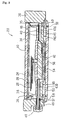
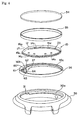
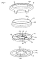
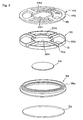
- Fig. 3 is a sectional view taken along line I-I of Fig. 2 of the watch, and Figs. 4 to 6 are exploded perspective views of the watch.
- a windshield 34 As shown in Figs. 3 and 4, in the upper part of the exterior casing 30, a windshield 34, a packing 35, the solar cell 10, and a solar cell holding member 36 are attached.
- a windshield 56 as a back, a pressing member 58, a movement holding member 50, a casing ring 44, a movement supporting member 40, and a cover ring 38 are attached.
- the scales 23 for indicating time as a component of the dial of the watch 20 are preliminarily formed by printing, marking, adhering or the like.
- the solar cell 10 is held by the ring-shaped solar cell holding member 36 and is fit in the exterior casing 30 from above.
- a stepped receiving portion 36a which engages with the periphery of the solar cell 10 to receive the solar cell 10 is formed.
- a notch 17 as a detent is formed in a part of the outer periphery of the solar cell 10, and a notch engagement portion 36b to engage with the notch 17 is formed in the solar cell holding member 36.
- a groove 37 penetrating the receiving portion 36a to the other side of the solar cell holding member 36 is formed in a portion where the notch engagement portion 36b of the solar cell holding member 36 is formed.
- a connection member 60 for supplying the power of the solar cell 10 to the movement 42 and the like is disposed in the groove 37.
- two contacts 61 and 62 are provided as a first contact portion pressed against the output terminals 16a and 16b (refer to Fig. 1) formed in the conductive portions 14c and 14b of the solar cell 10 when the solar cell 10 is assembled on the inside of the exterior casing 30 together with the solar cell holding member 36.
- Each of the contacts 61 and 62 is formed in a plate spring shape so as to assure the state of contact with the output terminals 16a and 16b with reliability to guarantee the supply of power from the solar cell 10 to the movement 42.
- a contact 63 to be conductive with the contact 61 and a contact 64 to be conductive with the contact 62 are provided on the other side of the connection member 60.
- Each of the contacts 63 and 64 is formed in a plate spring shape so as to be in contact with reliability in a state where they are pressed against not-illustrated input terminals on the positive and negative sides formed in a part of a conduction pattern 46.
- a flange-shaped receiving portion 30a is formed on the inside of the exterior casing 30 on the inside of the exterior casing 30 from above.
- the solar cell holding member 36 holding the solar cell 10 is fit in the exterior casing 30 from above, the solar cell holding member 36 is supported in the exterior casing 30 by the receiving portion 30a.
- the packing 35 is placed on the solar cell 10, and the windshield 34 is fit in the exterior casing 30 via the packing 35 and fixed.
- the windshield 34 may be fixed to the exterior casing 30 by adhesive or the like. In such a manner, the upper portion of the watch 20 is completed.
- the cover ring 38 has a cover portion 38a which is fit in the solar cell holding member 36 and hides the inner face of the solar cell holding member 36, and a flange portion 38b having an outside diameter almost the same as that of the inner face of the exterior casing 30.
- the ring-shaped movement supporting member 40 for supporting the movement 42 is disposed under the cover ring 38.
- the movement supporting member 40 includes an outer ring portion 40b having an outside diameter slightly smaller than the inside diameter of the exterior casing 30 and a disk-shaped supporting portion 40a for supporting the movement 42.
- the surface of the supporting portion 40a is finished in a manner similar to the dial of an ordinary watch.
- the diameter of the supporting portion 40a is preferably smaller than, at least, the length of the minute hand 26 of the watch 20 and, more preferably smaller than the length of the hour hand 24.
- the supporting portion 40a and the outer ring portion 40b are coupled to each other via four ribs 41 formed in the positions of 12 o'clock, 3 o'clock, 6 o'clock, and 9 o'clock of the watch 20.
- the sectional shape of the rib 41 is an inverted U shape.
- the portion of the inverted U shape serves as a path 41a.
- the number of the ribs 41 is not limited to four, but can be one to three, or five or more.
- the positions in which the ribs 41 are provided are not limited to the above positions but arbitrary proper positions can be selected in consideration of design of the watch 20 and the like.
- the casing ring 44 attached from below to the movement supporting member 40 has an inner ring portion 44a having a movement fitting portion 44c in which the movement 42 is to be fit, an outer ring portion 44b formed around the inner ring portion 44a, and ribs 45 for coupling the inner ring portion 44a and the outer ring portion 44b.
- the outer shape of the inner ring portion 44a is formed so as to be fit in a gap 41b between the movement 42 attached to the under face of the supporting portion 40a of the movement supporting member 40 and the ends of ribs 41.
- the outer ring portion 44b is formed in a size to be in contact with the inner face of the exterior casing 30 and in contact with the outer ring portion 40b of the movement supporting member 40.
- the ribs 45 are formed so as to be fit in the path 41a of the ribs 41 of the movement supporting member 40. In the rib 45 positioned in three o'clock of the watch 20 out of the four ribs 45 of the casing ring 44, an inverted U-shaped path 45a through which a winding stem 49 of a crown 48 can be inserted is formed.
- the movement holding member 50 has an outer ring portion 50b having the same outer shape as that of the outer ring portion 40b of the movement supporting member 40, a hole 50c to which the inner ring portion 44a of the casing ring 44 is fit, and an inner ring portion 50a having the same outside diameter as that of the supporting portion 40a of the movement supporting member 40.
- the inner ring portion 50a and the outer ring portion 50b are coupled to each other via four ribs 51 provided in the same positions as the ribs 41 of the movement supporting member 40.
- the sectional shape of the rib 51 is a U shape, and the U-shaped portion serves as a path 51a to which the rib 45 of the casing ring 44 is fit.
- the movement supporting member 40 and the movement holding member 50 formed as described above are overlapped with each other with the casing ring 44 sandwiched therebetween. Specifically, in a state where the rib 45 of the casing ring 44 is positioned in the path 41a of the movement supporting member 40 and the path 51a of the movement holding member 50, the inner ring portion 44a of the casing ring 44 is fit in the gap 41b (refer to Fig. 5) of the movement supporting member 40 and the hole 50c of the inner ring portion 50a of the movement holding member 50. By the operation, the outer ring portion 40b of the movement supporting member 40 and the outer ring portion 50b of the movement holding member 50 are fit on the inside of the outer ring portion 44b of the casing ring 44.
- the ribs 41 of the movement supporting member 40, ribs 45 of the casing ring 44, and ribs 51 of the movement holding member 50 form the rib parts 19a to 19d of the watch 20.
- the path 41a of the movement supporting member 40 and the path 51a of the movement holding member 50 in the position of 3 o'clock of the watch 20 form an inner path 43b (refer to Fig. 3) in the rib part 19b
- the paths 41a and 51a in the position of 9 o'clock form an inner path 43d of the rib part 19d.
- Figs. 7 (a) and 7 (b) are sectional views of the rib parts 19b and 19c, respectively, in a state where the movement supporting member 40, casing ring 44, and movement holding member 50 are assembled.
- Fig. 7 (a) is a sectional view taken along line II-II of Fig. 2
- Fig. 7 (b) is a sectional view taken along line III-III of Fig. 2.
- the rib 45 of the casing ring 44 is fit in both the path 41a of the rib 41 of the movement supporting member 40 and the path 51a of the rib 51 of the movement holding member 50, thereby preventing the movement supporting member 40 and the movement holding member 50 from rotating relative to each other.
- the winding stem 49 is provided through the inner path 43b of the rib part 19b in the position of 3 o'clock of the watch 20, and the sheet-type conduction pattern 46 for supplying the power of the solar cell 10 to the movement 42 is provided in the inner path 43d of the rib part 19d provided in the position of 9 o'clock of the watch 20.
- the conduction pattern 46 serves as the conductive member. The conduction pattern 46 is adhered on the rib 45 of the casing ring 44 constructing the rib part 19d.
- the winding stem 49 and the conduction pattern 46 may be provided in the separate rib parts 19b and 19d, respectively, as shown in Figs. 7 (a) and 7 (b) or in the same rib part, for example, the rib part 19b to which the winding stem 49 is inserted.
- the movement supporting member 40, casing ring 44, and movement holding member 50 assembled as described above construct an inner casing.
- the inner casing is fit into the exterior casing 30 from below.
- the ring-shaped pressing member 58 having a screw portion 58a is screwed in the exterior casing 30 via an O ring 57 from the lower side of the exterior casing 30.
- the movement supporting member 40, movement 42, casing ring 44, and movement holding member 50 are fixed in the exterior casing 30.
- the contacts 63 and 64 of the connection member 60 of the solar cell holding member 36 already assembled in the upper part of the exterior casing 30 come into contact with positive-side input terminal and negative-side input terminal (not shown) of the conductive pattern 46, so that the state where the power can be supplied from the solar cell 10 to the movement 42 is achieved.
- an identification plate 54 in which predetermined articles are written is adhered.
- the windshield 56 on the back face side is fit in the opening of the ring-shaped pressing member 58 via a packing 59.
- the watch 20 of the embodiment has resistance to water, maintained by the O ring 57 and packings 35 and 59.
- the windshield 56 may be fixed to the exterior casing 30 by, except for the packing 59, adhesive or the like.
- the space portion 32 extending in the radial direction of the watch 20 and penetrating in the perpendicular direction are formed between the rib parts 19a to 19d provided in the positions of 3 o'clock, 6 o'clock, 9 o'clock, and 12 o'clock, respectively. Further, since the transparent windshield 56 is used also as the back of the watch 20, novel design in which the watch is see-through can be obtained.
- the solar cell 10 may be provided on the back side (windshield 56 side). Moreover, a solar cell similar to the solar cell 10 may be additionally provided on the back side (windshield 56 side).
- the electromotive force can be obtained also by the solar cell provided on the back side.
- the solar batteries are provided on both the surface and back sides, even if the electromotive force of the solar cell 10 on the surface side is reduced, the reduced amount can be compensated by the electromotive force of the solar cell on the back side. Consequently, the line width of the photocell 18 in the solar cell 10 can be further reduced, or the interval S is further widened, thereby enabling the solar cell 10 to be formed more transparently.
- the diameter of the supporting portion 40a of the movement supporting member 40 is smaller than the length of each of the hour hand 24, minute hand 24, and second hand 28 of the watch 20, so that the tip of each of the pointers 24, 26, and 28 is projected from the supporting portion 40a and is seen from the back side of the watch 20.
- the scales 23 are provided in the transparent substrate 12 of the solar cell 10. Consequently, it is interesting for the user that time can be known also from the back side of the watch 20.
- the invention is not limited to the analog timepiece but can be also applied to a digital timepiece.
- Fig. 8 is a plan view of a second embodiment in which the present invention is applied to a digital watch.
- a digital display member 72 may be provided on a display plate 71 of a watch 70 or on the under face (back face) of the solar cell 10.
- the digital display member 72 may be formed directly on the transparent substrate 12 as a component of the solar cell 10. In this case, by using a polarizer as the transparent substrate 12, the polarizer of the digital display member 72 can be omitted.
- the solar cell 10 when an electronic device such as a watch is on or is to be put on a human body, the solar cell 10 can be effectively protected from electrical shock such as static electricity or the like built on the human body.
- the photocells 18 are disposed near the windshield 34 exposed in the surface of the watch like the solar cell 10 of the present invention, the possibility of incurring electrical shock by the static electricity is high. Since the photocells 18 are formed by stacking thin films of silicon or the like in the solar cell 10, when static electricity of a few thousand volts is directly applied to the photocells 18, due to occurrence of a pin hole or the like by internal discharge, an element may be destroyed.
- a transparent electrode film is formed on or near a cell substrate as a component of the solar cell 10 and the cell substrate is used for grounding.
- the cell substrate is used for grounding.
- Fig. 9 is a sectional view taken along line IV-IV of Fig. 2.
- Fig. 10 is a sectional view showing the configuration of the solar cell 10 in the embodiment.
- Fig. 11 is a plan view showing the shape of a conductive spring.
- a transparent electrode film (ITO film) 80 is formed on the back of the transparent substrate 12 as a component of the solar cell 10, that is, the face opposite to the face on which the photocells 18 are formed.
- ITO film 80 is formed on the back of the transparent substrate 12 as a component of the solar cell 10, that is, the face opposite to the face on which the photocells 18 are formed.
- a transparent electrode film (ITO film) 80 is formed on the back of the transparent substrate 12 as a component of the solar cell 10, that is, the face opposite to the face on which the photocells 18 are formed.
- a transparent electrode film (ITO film) 80 is formed on the back of the transparent substrate 12 as a component of the solar cell 10, that is, the face opposite to the face on which the photocells 18 are formed.
- a conductive spring 82 are provided in the top face of the exterior casing 30, not only the windshield 34, packing 35, solar cell 10 and solar cell holding member 36 but also a conductive spring 82 are provided.
- the scales 23 are provided on the transparent electrode film 80 and the solar cell 10 using the photocells 18 as elements is constructed on the face opposite to the scale 23 side.
- the transparent electrode film 80 is generally called a T.C.O. (abbreviation of Transparent Conductive Oxide) and ITO (abbreviation of Indium Tin Oxide) film is defined in a part of it.
- the ITO film is made of a mixture of stannic oxide (SnO 2 ) and indium oxide (InO 3 ) and can be generated by spraying or painting a liquid obtained by mixing powder-state fine crystal in a binder, or a method of coating a crystal ionized by vapor deposition.
- the thickness of a film generated is small, which is a few micrometers in the case of painting or is approximately 1000 to 2000 angstroms (approximately 0.01 to 0.02 micrometers) in the case of vapor deposition.
- the color is transparent but the characteristics slightly change according to the thickness or the wavelength of transmission light.
- the thickness used in the present invention is in a range where the change of transmittance of light spectrum in the case of transparent color decreases approximately 10 percent, that is, in a range from 1000 to 2000 angstroms (approximately 0.01 to 0.02 micrometers).
- the conductivity indicative of conducting performance of the transparent electrode film 80 is used in a range from a few ohms to a few k ⁇ in a surface resistance value for the reason that a resistance value equal to or smaller than the resistance value of the photocell 18 of the solar cell 10 is necessary.
- a transparent protective film 81 made of acrylic resin or the like covering the whole photocell 18 is formed on the photocell 18 side of the solar cell 10.
- the photocells 18 are partly exposed from the protective film 81 and output terminals 16a and 16b are formed in the portion.
- the output terminals 16a and 16b come into contact with the connection member 60 as shown in Fig. 9 so that the output of the solar cell 10 can be taken.
- the conductive spring 82 is provided so as to be in contact with the transparent electrode film 80 and is fixed by the windshield 34 via the packing 35.
- the conductive spring 82 is made by a thin-plate metal member. Although not shown, the conductive spring 82 has a shape curved in the vertical direction of Fig. 9. By being pressed from above by the windshield 34 via the packing 35, the conductive spring 82 is in pressure contact with the transparent electrode film 80 of the solar cell 10 and becomes conductive.
- the conductive spring 82 has an annular ring shape as Fig. 11 shows its plane shape.
- the conductive spring 82 has a plurality of projected conductive portions 82a on the outer periphery.
- the maximum outside diameter of the conductive spring 82 including the plurality of conductive portions 82a is set to be larger than the inside diameter of the exterior casing 30.
- the static electricity is discharged from the transparent electrode film 80 formed on the transparent substrate 12 of the solar cell 10 to the outside of the exterior casing 30 via the conductive spring 82 electrically connected to the exterior casing 30.
- the static electricity applied from the outside of the exterior casing 30, windshield 34, or the back made of plastic passes from the transparent electrode film 80 via the connection portion 82a of the conductive spring 82 conductive with the exterior casing 30 and returns to the exterior casing 30 before it is discharged to a part of the photocells 18 which are not conductive with the exterior casing 30.
- the solar cell 10 can be protected from a shock of the static electricity.
- the conductivity indicative of conducting performance of the transparent electrode film 80 when expressed in a surface resistance value, it lies in a range from a few ohms to a few k ⁇ .
- the resistance value is equivalent or smaller than the resistance value of the photocell 18 of the solar cell 10, so that the configuration in which the static electricity can be discharged to the transparent electrode film 80 side more easily is achieved.
- the third embodiment has been described on assumption that the transparent electrode film 80 is formed on the windshield 34 side of the transparent substrate 12 of the solar cell 10 and the solar cell 10 using the photocells 18 as elements is constructed on the movement 42 side, it is sufficient that an effect of bypassing the static electricity is obtained, so that the transparent electrode film 80 may be formed on the photocell 18 side via an insulating member. It may be formed on both surface and back including side faces of the transparent substrate. Further, it may be formed on the face of the windshield.
- the third embodiment has been described on assumption that the transparent electrode film 80 is formed on the solar cell 10 having high transparency in which the thin-line-shaped photocells 18 are formed.
- the photocell is constructed by a silicon thin film.
- a conductive member As a bypass.
- the transparent electrode film 80 as one of the conductive members may be constructed on the light incident side of the photocell 18 and the transparent electrode film 80 and the casing 30 serving as a ground are connected by using the conductive spring 82 or the like. With the configuration, there is an advantage that the flexibility of designing is increased.
- the watch has been described as an example of the electronic device, the present invention can be also applied to other timepieces such as a table clock and a wall clock. Further, the present invention can be applied to electronic devices other than timepieces.
- the solar cell 10 using the transparent substrate 12 as a base material is provided under the windshield 34 of the watch 20, by forming the thin-line-shaped photocells 18 directly on the windshield 34, the thickness of the watch 20 can be reduced.
- the cell substrate as a component of the solar cell has been described as an entirely transparent substrate. However, it is sufficient that at least the portion in which the photocells are formed is transparent, and the peripheral portion in which the conductive portions are formed may be opaque.
- the transparency of the solar cell can be improved.
- the flexibility in designing electronic devices, particularly, timepieces can be largely improved.
- the electronic device can be protected from external environments such as static electricity built on a human body, so that a durable electronic device can be provided.
- the present invention is not limited to a watch but can be applied to electronic devices, each operating on a solar cell as a power source, of kinds in a wide range small communication devices such as a portable telephone and a portable radio, and a pedometer, a portable hemadynamometer, a radio and the like.
Landscapes
- Engineering & Computer Science (AREA)
- Power Engineering (AREA)
- Physics & Mathematics (AREA)
- General Physics & Mathematics (AREA)
- Electric Clocks (AREA)
- Electromechanical Clocks (AREA)
- Photovoltaic Devices (AREA)
Abstract
Description
Claims (38)
- An electronic device having a solar cell and a unit driven by a power generated by the solar cell, wherein the solar cell is a translucent solar cell comprising:a transparent cell substrate;a plurality of conductive portions provided around the cell substrate and connected in series; anda plurality of photocells, each having a thin-line shape, formed at proper intervals on the cell substrate and connected to the conductive portions.
- The electronic device according to claim 1, wherein the photocells each having a thin-line shape are formed on the cell substrate at regular intervals.
- The electronic device according to claim 1 or 2, wherein the photocell having a thin-line shape is formed so as to extend from one of the conductive portions in a direction crossing the cell substrate.
- The electronic device according to claim 3, wherein the photocells each having a thin-line shape extend so as to cross the cell substrate to a position near the corresponding conductive portion.
- The electronic device according to any one of claims 1 to 4, wherein the photocells are connected to the conductive portions so that the same electromotive force is obtained from each of the plurality of conductive portions.
- The electronic device according to claim 5, wherein the photocells are connected to the conductive portions so that the total areas of the photocells connected to the conductive portions are equal to each other.
- The electronic device according to any one of claims 1 to 6, wherein the photocell of a thin-line shape has a width in a range from 3% to 30% of an interval.
- The electronic device according to any one of claims 1 to 7, wherein a part of the conductive portions is formed as an output terminal for supplying power from the translucent solar cell to the unit.
- The electronic device according to any one of claims 1 to 8, wherein the unit includes a display member for displaying predetermined data.
- The electronic device according to claim 9, wherein the translucent solar cell is disposed on the upper side of the display member.
- The electronic device according to claim 10, wherein the display member includes a liquid crystal display.
- The electronic device according to claim 10 or 11, wherein the display member is provided on the back face of the cell substrate.
- The electronic device according to any one of claims 1 to 12, wherein the translucent solar cell is disposed on the upper side of a casing of the electronic device, the unit is disposed below the translucent solar cell in the casing, a space is created between the unit and the casing, and a transparent member is disposed under the electronic device, so that the electronic device is see-through.
- The electronic device according to claim 13, wherein the translucent solar cell is disposed, not on the upper side of the casing but, on the lower side of the casing or the translucent solar batteries are disposed on both the upper and lower sides of the casing.
- The electronic device according to any one of claims 9 to 11, wherein the electronic device is a timepiece and the display member includes a time display member indicating time.
- The electronic device according to claim 15, wherein the display member includes an analog display member for displaying time by pointers and a dial, and the translucent solar cell is provided above the dial.
- The electronic device according to claim 16, wherein the cell substrate is larger than the outer periphery of a movement for driving the pointers of the analog display member.
- The electronic device according to claim 16 or 17, wherein the translucent solar cell is provided above the pointers.
- The electronic device according to any one of claims 16 to 18, wherein a scale of the dial is provided on the surface or back of the cell substrate.
- The electronic device according to any one of claims 15 to 19, wherein the cell substrate is a windshield of the timepiece.
- The electronic device according to any one of claims 16 to 20, wherein the translucent solar cell is disposed on the surface of a casing of the timepiece, the pointers of the analog display member and the movement for driving the pointers are disposed below the translucent solar cell in the casing, a space is created between the movement and the casing, and a transparent plate is disposed on the under face side of the timepiece, so that the timepiece is see-through.
- The electronic device according to claim 21, wherein the translucent solar cell is disposed, not on the surface of the casing but, on the back side of the casing or the translucent solar batteries are disposed on both the surface of the casing and the back side.
- The electronic device according to claim 21 or 22, wherein the casing and the movement are coupled to each other via one or a plurality-of ribs, and the movement is supported on the center side of the casing.
- The electronic device according to claim 23, wherein the casing has an exterior casing and an inner casing fit in the exterior casing, and the rib is formed in the inner casing.
- The electronic device according to claim 23 or 24, wherein a conductive member for supplying the power from the translucent solar cell to the movement through the inside of the rib is disposed.
- The electronic device according to any one of claims 23 to 25, wherein a winding stem is provided so as to be inserted in the rib.
- The electronic device according to claim 25, wherein the conductive member is provided through a rib different from the rib through which the winding stem is inserted.
- The electronic device according to any one of claims 25 to 27, wherein the conductive portion of the cell substrate and the conductive member are connected to each other via a connection member, and this connection member has a first contact portion abutted against an output terminal of the conductive portion, and a second contact portion abutted against the conductive member.
- The electronic device according to claim 28, wherein the solar cell is held in a solar cell holding member fit in the casing, the connection member is provided for the solar cell holding member, the first contact portion comes into contact with an output terminal of the conductive portion of the solar cell in a receiving portion of the solar cell holding member for receiving the solar cell, and the second contact portion comes into contact with the conductive member when the solar cell holding member is housed in the casing.
- The electronic device according to any one of claims 21 to 29, wherein at least a minute hand indicating minute(s) out of the pointers of the analog display member is extended to a position above the space created between the casing and the movement.
- The electronic device according to any one of claims 15 to 30, wherein the size of the translucent solar cell is made larger than that of the display member.
- The electronic device according to any one of claims 16 to 31, wherein a portion having an inside diameter smaller than that of the cell substrate is provided in the casing, and the conductive portion provided for the cell substrate is hidden by this portion.
- The electronic device according to any one of claims 1 to 32, wherein a transparent electrode film is formed on or near the cell substrate, and the transparent electrode film is connected to the ground of the unit.
- The electronic device according to claim 33, wherein the transparent electrode film is formed on the side opposite to a face on which a photocell is formed of the cell substrate.
- The electronic device according to claim 34, wherein the transparent electrode film is formed on a substrate face opposite to a face on which a photocell is formed of the cell substrate.
- The electronic device according to claim 33, wherein the transparent electrode film is formed on the side of a face on which a photocell is formed of the cell substrate.
- The electronic device according to any one of claims 33 to 36, wherein the transparent electrode film is grounded to the casing via the conductive member.
- The electronic device according to any one of claims 33 to 37, wherein the transparent electrode film is a transparent ITO thin film.
Applications Claiming Priority (5)
| Application Number | Priority Date | Filing Date | Title |
|---|---|---|---|
| JP2000078920 | 2000-03-21 | ||
| JP2000078920A JP4607277B2 (en) | 2000-03-21 | 2000-03-21 | Electronics |
| JP2000295941 | 2000-09-28 | ||
| JP2000295941A JP4559605B2 (en) | 2000-09-28 | 2000-09-28 | Electronics |
| PCT/JP2001/002091 WO2001071434A1 (en) | 2000-03-21 | 2001-03-16 | Electronic unit |
Publications (3)
| Publication Number | Publication Date |
|---|---|
| EP1186966A1 true EP1186966A1 (en) | 2002-03-13 |
| EP1186966A4 EP1186966A4 (en) | 2007-01-24 |
| EP1186966B1 EP1186966B1 (en) | 2018-08-08 |
Family
ID=26587995
Family Applications (1)
| Application Number | Title | Priority Date | Filing Date |
|---|---|---|---|
| EP01912422.1A Expired - Lifetime EP1186966B1 (en) | 2000-03-21 | 2001-03-16 | Electronic unit |
Country Status (3)
| Country | Link |
|---|---|
| US (1) | US6521822B2 (en) |
| EP (1) | EP1186966B1 (en) |
| WO (1) | WO2001071434A1 (en) |
Cited By (1)
| Publication number | Priority date | Publication date | Assignee | Title |
|---|---|---|---|---|
| FR3089346A1 (en) * | 2018-11-30 | 2020-06-05 | Sunpartner Technologies | Texturing of the front electrode in a semi-transparent photovoltaic module in order to control the colorimetric aspect |
Families Citing this family (27)
| Publication number | Priority date | Publication date | Assignee | Title |
|---|---|---|---|---|
| WO2002039504A1 (en) * | 2000-11-10 | 2002-05-16 | Citizen Watch Co., Ltd. | Solar cell module and portable electronic apparatus with it |
| US6714488B1 (en) * | 2001-09-04 | 2004-03-30 | Eric J. Vogel | Kinetichrome |
| KR200292687Y1 (en) * | 2002-07-15 | 2002-10-25 | 복 권 이 | Removable wristwatch for static electricity |
| WO2004055605A1 (en) * | 2002-12-16 | 2004-07-01 | Citizen Watch Co., Ltd. | Electronic timepiece with solar cell |
| WO2004066042A1 (en) * | 2003-01-23 | 2004-08-05 | Citizen Watch Co., Ltd. | Electronic timepiece with solar cell |
| US8798531B2 (en) * | 2007-02-14 | 2014-08-05 | Kaba Ag | System and portable device for transmitting identification signals |
| KR20090121629A (en) * | 2008-05-22 | 2009-11-26 | 삼성전자주식회사 | Solar cell and solar cell module using same |
| WO2010076944A1 (en) * | 2008-12-30 | 2010-07-08 | 네오뷰코오롱 주식회사 | Electronic watch |
| US8096702B2 (en) * | 2009-05-28 | 2012-01-17 | The Avalanche Group, Llc | Ornament container for watch |
| JP5866860B2 (en) * | 2011-01-05 | 2016-02-24 | セイコーエプソン株式会社 | Clock with wireless function |
| JP5715506B2 (en) * | 2011-06-15 | 2015-05-07 | セイコーインスツル株式会社 | Electronic equipment with solar cells |
| EP2574995B1 (en) * | 2011-09-28 | 2020-06-17 | ETA SA Manufacture Horlogère Suisse | Electromechanical timepiece with an additional function |
| JP5888071B2 (en) * | 2012-04-02 | 2016-03-16 | カシオ計算機株式会社 | Solar power generator and electronic watch |
| US20140159638A1 (en) * | 2012-08-19 | 2014-06-12 | EnergyBionics, LLC | Portable energy harvesting, storing, and charging device |
| JP6048222B2 (en) * | 2013-03-04 | 2016-12-21 | カシオ計算機株式会社 | Solar panels and watches |
| JP6269945B2 (en) * | 2013-09-04 | 2018-01-31 | カシオ計算機株式会社 | Solar panels and watches |
| JP6442503B2 (en) * | 2014-06-24 | 2018-12-19 | シチズン時計株式会社 | Electronic watch with solar cell |
| US9630652B2 (en) | 2015-03-04 | 2017-04-25 | Fca Us Llc | Vehicle pillar reinforcement construction for side impact |
| JP6740574B2 (en) * | 2015-07-22 | 2020-08-19 | セイコーエプソン株式会社 | clock |
| CN105159046B (en) * | 2015-09-08 | 2017-12-01 | 上海和辉光电有限公司 | A kind of pointer intelligent watch and its display methods |
| HRP20201797T1 (en) * | 2015-10-30 | 2021-01-08 | Tropiglas Technologies Ltd | A panel structure for receiving light and generating electricity |
| US9791833B1 (en) * | 2016-04-13 | 2017-10-17 | Google Inc. | Physical watch hands for a computerized watch |
| JP6763415B2 (en) * | 2018-03-14 | 2020-09-30 | カシオ計算機株式会社 | Solar panels, display devices and clocks |
| JP6891914B2 (en) * | 2019-03-26 | 2021-06-18 | カシオ計算機株式会社 | Solar panels, display devices and clocks |
| JP6927245B2 (en) * | 2019-03-26 | 2021-08-25 | カシオ計算機株式会社 | Solar panels, display devices and clocks |
| JP7786093B2 (en) * | 2021-09-16 | 2025-12-16 | セイコーエプソン株式会社 | clock |
| EP4517837A1 (en) * | 2023-08-28 | 2025-03-05 | ETA SA Manufacture Horlogère Suisse | Photovoltaic cell with a specific arrangement of energy collectors, and method for producing such a cell |
Family Cites Families (17)
| Publication number | Priority date | Publication date | Assignee | Title |
|---|---|---|---|---|
| JPS5677885A (en) * | 1979-11-28 | 1981-06-26 | Citizen Watch Co Ltd | Liquid crystal display unit |
| JPS5794964A (en) | 1980-12-01 | 1982-06-12 | Nec Corp | Magnetic disk device |
| JPS5794964U (en) * | 1980-12-02 | 1982-06-11 | ||
| JPS57201878A (en) * | 1981-06-08 | 1982-12-10 | Seiko Epson Corp | Solar battery watch |
| JPS63181989A (en) | 1987-01-23 | 1988-07-27 | Tec:Kk | Automatic cold brine treatment equipment |
| JPS63181989U (en) * | 1987-05-15 | 1988-11-24 | ||
| JPH06508441A (en) * | 1992-03-26 | 1994-09-22 | アスラブ ソシエテ アノニム | A horological piece that has an energy source and is composed of photovoltaic cells. |
| JPH07287081A (en) * | 1994-04-18 | 1995-10-31 | Citizen Watch Co Ltd | Connection structure for solar cell |
| US5880796A (en) * | 1996-07-12 | 1999-03-09 | Casio Computer Co., Ltd. | Display device with display plate having metal upper suface including narrow outgoing opening for emitting light from light emitting member |
| US6122226A (en) * | 1996-09-05 | 2000-09-19 | Citizen Watch Co., Ltd. | Combination electronic watch |
| JPH10270735A (en) * | 1997-03-28 | 1998-10-09 | Sharp Corp | Solar cell and method of manufacturing the same |
| EP1058224B1 (en) | 1998-11-10 | 2006-10-11 | Citizen Watch Co. Ltd. | Electronic device with solar cell |
| EP1126337A4 (en) | 1998-11-26 | 2002-04-17 | Citizen Watch Co Ltd | Timepiece |
| JP2000162342A (en) * | 1998-11-30 | 2000-06-16 | Sanyo Electric Co Ltd | Clock with solar cell |
| JP2000221282A (en) * | 1999-01-29 | 2000-08-11 | Citizen Watch Co Ltd | Time piece |
| JP3983911B2 (en) | 1998-12-22 | 2007-09-26 | シチズンホールディングス株式会社 | Liquid crystal display |
| JP3906956B2 (en) | 1998-12-24 | 2007-04-18 | 株式会社 日立ディスプレイズ | Liquid crystal display |
-
2001
- 2001-03-16 WO PCT/JP2001/002091 patent/WO2001071434A1/en not_active Ceased
- 2001-03-16 EP EP01912422.1A patent/EP1186966B1/en not_active Expired - Lifetime
- 2001-03-16 US US09/959,096 patent/US6521822B2/en not_active Expired - Lifetime
Cited By (1)
| Publication number | Priority date | Publication date | Assignee | Title |
|---|---|---|---|---|
| FR3089346A1 (en) * | 2018-11-30 | 2020-06-05 | Sunpartner Technologies | Texturing of the front electrode in a semi-transparent photovoltaic module in order to control the colorimetric aspect |
Also Published As
| Publication number | Publication date |
|---|---|
| US20020157700A1 (en) | 2002-10-31 |
| US6521822B2 (en) | 2003-02-18 |
| WO2001071434A1 (en) | 2001-09-27 |
| EP1186966A4 (en) | 2007-01-24 |
| EP1186966B1 (en) | 2018-08-08 |
Similar Documents
| Publication | Publication Date | Title |
|---|---|---|
| US6521822B2 (en) | Electronic unit | |
| CN105531633B (en) | Solar panels and the clock and watch including solar panels | |
| EP1126337A1 (en) | Timepiece | |
| US20250110449A1 (en) | Solar panel, display device, and timepiece | |
| JP2007170995A (en) | Electronic equipment and electronic timepiece | |
| CN106354007B (en) | Antenna and clock and watch | |
| JPWO2002039504A1 (en) | Solar cell module and portable electronic device equipped with the same | |
| CN115712232A (en) | Display device and timepiece | |
| JP6927245B2 (en) | Solar panels, display devices and clocks | |
| US6243259B1 (en) | Electronic member and electronic device | |
| JP4559605B2 (en) | Electronics | |
| JP7334761B2 (en) | Solar panels, displays and clocks | |
| JP2025176176A (en) | Manufacturing method of electronic watch and solar panel | |
| US9170566B2 (en) | Watch including a flange | |
| JP2020013844A (en) | Photoelectric conversion element, photoelectric conversion module and electronic device | |
| JP4607277B2 (en) | Electronics | |
| JP2545233Y2 (en) | Key input device | |
| CN114631195B (en) | Solar panels, electronic devices and electronic clocks | |
| JP7131588B2 (en) | clock | |
| JP4814007B2 (en) | clock | |
| JP4244137B2 (en) | Solar cell module and electronic device | |
| JP2004333239A (en) | Electronics | |
| JPS647589Y2 (en) | ||
| CN122002910A (en) | Photovoltaic cell and manufacturing method thereof, display screen and electronic equipment | |
| KR19990016079U (en) | Smart card |
Legal Events
| Date | Code | Title | Description |
|---|---|---|---|
| PUAI | Public reference made under article 153(3) epc to a published international application that has entered the european phase |
Free format text: ORIGINAL CODE: 0009012 |
|
| 17P | Request for examination filed |
Effective date: 20011113 |
|
| AK | Designated contracting states |
Kind code of ref document: A1 Designated state(s): AT BE CH CY DE DK ES FI FR GB GR IE IT LI LU MC NL PT SE TR |
|
| AX | Request for extension of the european patent |
Free format text: AL;LT;LV;MK;RO;SI |
|
| RBV | Designated contracting states (corrected) |
Designated state(s): DE FR GB IT |
|
| A4 | Supplementary search report drawn up and despatched |
Effective date: 20061221 |
|
| RIC1 | Information provided on ipc code assigned before grant |
Ipc: G04C 10/02 20060101AFI20011002BHEP |
|
| RAP1 | Party data changed (applicant data changed or rights of an application transferred) |
Owner name: CITIZEN HOLDINGS CO., LTD. |
|
| 17Q | First examination report despatched |
Effective date: 20080523 |
|
| RAP1 | Party data changed (applicant data changed or rights of an application transferred) |
Owner name: CITIZEN WATCH CO., LTD. |
|
| REG | Reference to a national code |
Ref country code: DE Ref legal event code: R079 Ref document number: 60150901 Country of ref document: DE Free format text: PREVIOUS MAIN CLASS: G04C0010020000 Ipc: H01L0031020000 |
|
| GRAP | Despatch of communication of intention to grant a patent |
Free format text: ORIGINAL CODE: EPIDOSNIGR1 |
|
| STAA | Information on the status of an ep patent application or granted ep patent |
Free format text: STATUS: GRANT OF PATENT IS INTENDED |
|
| RIC1 | Information provided on ipc code assigned before grant |
Ipc: H01L 31/02 20060101AFI20180129BHEP Ipc: H01L 31/0468 20140101ALI20180129BHEP Ipc: G04C 10/02 20060101ALI20180129BHEP Ipc: H01L 31/048 20140101ALI20180129BHEP Ipc: H01L 31/046 20140101ALI20180129BHEP Ipc: H01L 31/0352 20060101ALI20180129BHEP |
|
| INTG | Intention to grant announced |
Effective date: 20180221 |
|
| GRAS | Grant fee paid |
Free format text: ORIGINAL CODE: EPIDOSNIGR3 |
|
| GRAA | (expected) grant |
Free format text: ORIGINAL CODE: 0009210 |
|
| STAA | Information on the status of an ep patent application or granted ep patent |
Free format text: STATUS: THE PATENT HAS BEEN GRANTED |
|
| AK | Designated contracting states |
Kind code of ref document: B1 Designated state(s): DE FR GB IT |
|
| REG | Reference to a national code |
Ref country code: GB Ref legal event code: FG4D |
|
| REG | Reference to a national code |
Ref country code: DE Ref legal event code: R096 Ref document number: 60150901 Country of ref document: DE |
|
| RIC2 | Information provided on ipc code assigned after grant |
Ipc: H01L 31/0468 20140101ALI20180129BHEP Ipc: H01L 31/046 20140101ALI20180129BHEP Ipc: H01L 31/0352 20060101ALI20180129BHEP Ipc: H01L 31/02 20060101AFI20180129BHEP Ipc: H01L 31/048 20140101ALI20180129BHEP Ipc: G04C 10/02 20060101ALI20180129BHEP |
|
| PG25 | Lapsed in a contracting state [announced via postgrant information from national office to epo] |
Ref country code: IT Free format text: LAPSE BECAUSE OF FAILURE TO SUBMIT A TRANSLATION OF THE DESCRIPTION OR TO PAY THE FEE WITHIN THE PRESCRIBED TIME-LIMIT Effective date: 20180808 |
|
| PGFP | Annual fee paid to national office [announced via postgrant information from national office to epo] |
Ref country code: FR Payment date: 20190322 Year of fee payment: 19 Ref country code: GB Payment date: 20190320 Year of fee payment: 19 Ref country code: DE Payment date: 20190321 Year of fee payment: 19 |
|
| REG | Reference to a national code |
Ref country code: DE Ref legal event code: R097 Ref document number: 60150901 Country of ref document: DE |
|
| PLBE | No opposition filed within time limit |
Free format text: ORIGINAL CODE: 0009261 |
|
| STAA | Information on the status of an ep patent application or granted ep patent |
Free format text: STATUS: NO OPPOSITION FILED WITHIN TIME LIMIT |
|
| 26N | No opposition filed |
Effective date: 20190509 |
|
| REG | Reference to a national code |
Ref country code: DE Ref legal event code: R119 Ref document number: 60150901 Country of ref document: DE |
|
| PG25 | Lapsed in a contracting state [announced via postgrant information from national office to epo] |
Ref country code: DE Free format text: LAPSE BECAUSE OF NON-PAYMENT OF DUE FEES Effective date: 20201001 Ref country code: FR Free format text: LAPSE BECAUSE OF NON-PAYMENT OF DUE FEES Effective date: 20200331 |
|
| GBPC | Gb: european patent ceased through non-payment of renewal fee |
Effective date: 20200316 |
|
| PG25 | Lapsed in a contracting state [announced via postgrant information from national office to epo] |
Ref country code: GB Free format text: LAPSE BECAUSE OF NON-PAYMENT OF DUE FEES Effective date: 20200316 |