EP1186923A2 - Device for aligning optical source and optical fiber in optical source module - Google Patents
Device for aligning optical source and optical fiber in optical source module Download PDFInfo
- Publication number
- EP1186923A2 EP1186923A2 EP01115008A EP01115008A EP1186923A2 EP 1186923 A2 EP1186923 A2 EP 1186923A2 EP 01115008 A EP01115008 A EP 01115008A EP 01115008 A EP01115008 A EP 01115008A EP 1186923 A2 EP1186923 A2 EP 1186923A2
- Authority
- EP
- European Patent Office
- Prior art keywords
- optical fiber
- optical
- saddle
- fiber ferrule
- optical source
- Prior art date
- Legal status (The legal status is an assumption and is not a legal conclusion. Google has not performed a legal analysis and makes no representation as to the accuracy of the status listed.)
- Granted
Links
Images





Classifications
-
- G—PHYSICS
- G02—OPTICS
- G02B—OPTICAL ELEMENTS, SYSTEMS OR APPARATUS
- G02B6/00—Light guides; Structural details of arrangements comprising light guides and other optical elements, e.g. couplings
- G02B6/24—Coupling light guides
- G02B6/42—Coupling light guides with opto-electronic elements
- G02B6/4201—Packages, e.g. shape, construction, internal or external details
- G02B6/4219—Mechanical fixtures for holding or positioning the elements relative to each other in the couplings; Alignment methods for the elements, e.g. measuring or observing methods especially used therefor
-
- G—PHYSICS
- G02—OPTICS
- G02B—OPTICAL ELEMENTS, SYSTEMS OR APPARATUS
- G02B6/00—Light guides; Structural details of arrangements comprising light guides and other optical elements, e.g. couplings
- G02B6/24—Coupling light guides
- G02B6/42—Coupling light guides with opto-electronic elements
- G02B6/4201—Packages, e.g. shape, construction, internal or external details
- G02B6/4219—Mechanical fixtures for holding or positioning the elements relative to each other in the couplings; Alignment methods for the elements, e.g. measuring or observing methods especially used therefor
- G02B6/4236—Fixing or mounting methods of the aligned elements
- G02B6/4237—Welding
Definitions
- the present invention relates generally to an optical source module and, in particular, to a device for aligning an optical source and an optical fiber in the optical source module.
- an optical source module is essential in all aspects of transmitting and receiving an optical signal in an optical communications system.
- an optical source module is typically used as a pump laser diode module, semiconductor optical-amplifier module, and for transmitting/receiving module in the range of 155Mbit and 2.5Gbit.
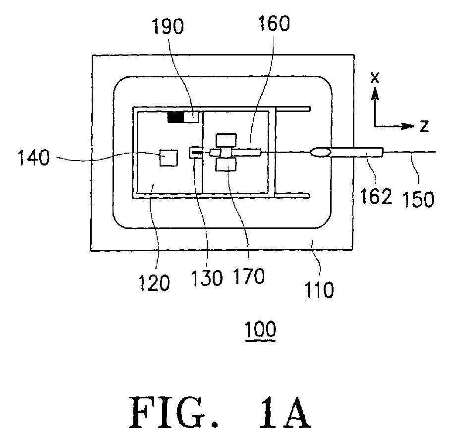
- FIG. 1a is a top view illustrating the construction of a conventional optical source module.
- FIG. 1b is a side view illustrating the construction of the conventional optical source module.
- the conventional optical source module 100 comprises a housing 110, a substrate 120, a laser diode 130, a photo diode 140, an optical fiber 150, an optical ferrule 160, a saddle 170, a thermoelectric cooler 180, a thermister 190, and, a window ferrule 162.
- the laser diode 130 and an optical fiber 150 are aligned according to the following steps. First, the laser diode 130 is mounted on the substrate 120. Then, the optical fiber 150 and the optical ferrule 160 are soldered together, and the lower portion of the saddle 170 is mounted on the substrate 120. Thereafter, when electric power is supplied to the laser diode 130 to emit light, the position of the optical ferrule 160 is adjusted to realize a maximum light-receiving position. Once the maximum light-receiving position is determined, the saddle 170 and the optical ferrule 160 are welded together. Here, the thermal distortion caused by this welding process should be within an alignment allowable error range.
- a lens having the same shape as archenterons of the laser diode is processed at one end of the optical fiber for a precise alignment in six axes.
- the error range of an axis should be within the least allowable error range, which is preferably less than 0.2 m.
- FIG. 2a is a side view illustrating a device for aligning an optical source and an optical fiber according to a first embodiment of the conventional art.
- FIG. 2b is a front view of the device in FIG. 2a.
- FIG. 3 is a side view magnifying an optical ferrule and saddles of the device in FIG. 2a.
- FIG. 4 is a side view magnifying an optical ferrule and saddles of the device in accordance with a second embodiment of the conventional art.
- the saddles 170 and 270 of the device for aligning the optical source and the optical fiber according to the first and second embodiments of the conventional art are thermally distorted to a degree of 5 to 20 m in an y-axis (vertical) direction due to the heat applied to the respective welded sections S.
- the heat is conducted toward the arrow direction, as shown in FIGs. 3 and 4.
- the optical ferrule 160 including the optical fiber 150 is displaced downward in a vertical direction, the vertically-downward displacement of the optical ferrule 160 decreases optical coupling efficiency between the optical source and the optical fiber, thereby impeding reliability of the optical source module.
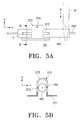
- FIG. 5a is the side view of a device for aligning an optical source and an optical fiber according to a third embodiment of the conventional art.
- FIG. 5b is a view illustrating the cross section line B-B' in FIG. 5a.
- FIG. 6a is a side view of the device for aligning an optical source and an optical fiber according to a forth embodiment of the conventional art.
- FIG. 6b is a view illustrating the cross section line A-A' in FIG. 6a.
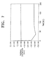
- FIG. 7 is a graph illustrating the thermal distortion of the device according to the third and forth embodiments of the conventional art.
- the horizontal axis represents time
- the vertical axis represents the degree of thermal distortion, respectively.
- the saddles 370 and 470 of the device according to the third and forth embodiments of the conventional art includes arms 372 and 473 formed with distance from bases 371 and 471, respectively.
- the saddles 370 and 470 exhibit a relatively small value of 0.4 m in thermal distortion in the y-axis direction as shown in FIG. 7.
- the degree of thermal distortion is greater than the allowable error range, which should be less than 0.2 m for thermal distortion in the vertical direction for optimal performance.
- the optical ferrule 160 is frequently removed using a gripper to re-align the optical ferrule 160, and such an operation is a time-consuming process and cumbersome during the manufacturing process.
- a residual stress which occurs during the fabrication process should be minimized to enhance the durability of the optical source module.
- an object of the present invention to provide a device for aligning an optical source and an optical fiber in an optical source module to minimize a thermal distortion and residual stress caused by the welding of the optical fiber ferrule and the saddle member.
- FIG. 8 is a cross-sectional view illustrating an optical ferrule 160 and a saddle member 500 in an optical source module that is used for aligning an optical source and optical fiber 150 according to the preferred embodiment of the present invention.
- the optical source module includes a substrate (not shown); an optical light source (not shown) mounted on the substrate; an optical fiber 150 for receiving light emitted from the optical light source; an optical fiber ferrule 160 for supporting the optical fiber 150; and, a saddle member 500 mounted on the substrate for supporting the optical fiber ferrule 160.
- FIG. 9 is a side view of the optical ferrule and the saddle for aligning an optical source and an optical fiber according to the preferred embodiment of the present invention.
- FIG. 10 is a view illustrating the cross-section line B-B' in FIG. 9.
- the saddle 500 of the inventive device for aligning an optical source and optical fiber includes: a pair of elongated bases 510 spaced apart from each other in a parallel relationship so that the optical fiber ferrule 160 can be disposed between the bases 510; a sub rib 520 extending upwardly from the inside ends of the respective base 510 in a normal direction; a center rib 530 with a smaller width than the sub rib 520 extending upwardly from the center of the respective sub rib 520; an arm member 540 with a greater width than the center rib 530 extending from the respective center rib 530 and positioned near the optical fiber ferrule 160 along the center axis of the optical fiber ferrule 160, each arm 540 having a pair of welded sections S at both ends for coupling the optical fiber ferrule 160 thereto; a reinforcing member 550 with tapered side ends extending from the top end of the respective center rib 530; and, a loop
- the installation process of the saddle 500 is performed in the following steps. First, the respective base 510 of the saddle 500 with the optical fiber ferrule 160 displaced therein are mounted on a substrate (not shown) using a displacement device 10. Next, an electric power is supplied to a laser diode (not shown) mounted on the substrate near the saddle 500. Then, the position of the optical fiber ferrule 160 is adjusted to determine a maximum light-receiving position. Once the maximum light-receiving position is determined, the welded sections S formed at the ends of the arms 540 are laser-welded to couple the saddle 500 to the optical fiber ferrule 160.
- the heat applied to the welded sections S of the arms 540 for coupling is conducted through the reinforcing sections 550, the center ribs 530, the loop 560, etc., through the arms 540. Also, the heat conduction and residual stress caused by the cooling process after welding are directed to the bases 510, e.g., vertically downward, are minimized because of the spacing, c, between the arms 540 and the sub ribs 520 as well as of the reinforcing sections 550.
- the same material for the substrate and optical fiber ferrule is used to prepare the saddle 500 to minimize thermal expansion and contraction during the welding process.
- the material preferably should have a lower linear expansion.
- Ni, KOVAR, Fe-Ni alloy, and SUS3041 can be used as the material for the saddle.
- FIG. 11 is a cross-sectional view illustrating an optical ferrule and saddle of the inventive device for aligning an optical source and an optical fiber according to a second preferred embodiment of the present invention.
- FIG. 12 is a side view illustrating the inventive device according to the second preferred embodiment of the present invention.
- FIG. 13 is a view illustrating the cross-section line C-C' in FIG. 12.
- the saddle member 600 of the inventive device for aligning an optical source and an optical fiber includes: plate-shaped bases 610; a sub-rib member 620 spaced apart from each other and extending from the upper surface of the respective base 610 so that the optical fiber ferrule 160 can be inserted therebetween; a center rib 630 with a smaller width than the sub-rib member 620 extending upwardly from the respective center portion of the sub-rib member 620; an elongated arm 640 having welded section S for coupling the optical fiber ferrule 160 at each end of the arm 640, extending from the center ribs 630 in a vertical direction, and displaced along the longitudinal direction of the optical fiber ferrule 160; and a reinforcing member 650 with tapered side ends extending in a vertical direction from the respective the arm 64.
- the saddle member 600 of the second preferred embodiment of the present invention has bases 610 monolithic-structured without the loop member 560 of FIG. 8 for connecting the respective center ribs together.
- the installation method of the saddle 600 according to the second preferred embodiment of the present invention is performed according to the following steps. First, the bases 610 are mounted on a substrate (not shown). An electric power is supplied to a laser diode (not shown) located on the same substrate; then the position of the optical fiber ferrule 160 is adjusted so as to determine a maximum light-receiving position. Once the maximum light-receiving position is determined, the welded sections S formed at the ends of the arms 640 are laser-welded to couple the saddle 600 to the optical fiber ferrule 160.
- the heat applied to the welded sections S of the arms 640 is conducted through the reinforcing sections 650, the center ribs 630, etc., through the arms 640.
- the heat conduction and residual stress directed to the bases 610 e.g., vertically downward, are minimized because of the spacing c between the arms 640 and the sub ribs 620 as well as the reinforcing sections 650.
- the numeric values of the detailed design e.g., a distance a between one end 150 of the optical fiber and one end of the arm, a distance b between one end of the arm and the other end of the arm, a spacing c between the arm and the sub rib as well as a width d of the reinforcing section may be determined through a test or simulation to obtain a desired result.
- the contact positions between the arms and the sub ribs are formed to have a taper shape or a round shape for easy processing thereof.
- the same material as the substrate and the optical fiber ferrule is used for the saddle as in the first preferred embodiment of the present invention to minimize the welding and the thermal distortion.
- the material has preferably a lower linear expansion.
- Ni, KOVAR, Fe-Ni alloy, and SUS3041 are used as the material of the saddle.
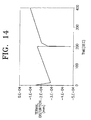
- FIG. 14 is a graph illustrating the thermal distortion result obtained through the inventive device according to the first and second embodiments of the present invention.
- the horizontal axis represents time, and the vertical axis represents the degree of the thermal distortion.
- the welded sections S of the inventive device for aligning an optical source and an optical fiber exhibits a lower thermal distortion of 0.02 m, whi ch is much smaller than the prior art system, which exhibited thermal distortion of 0.4 m.
- the inventive device can maintain an alignment precision within the allowable error range that is less than 0.2 m, thus allowing optical coupling efficiency between the optical source and the optical fiber to be higher than 95%.
- the device for aligning an optical source and an optical fiber has advantages of maintaining a higher optical coupling efficiency between the optical source and the optical fiber as well as securing a long-term durability of the optical source module by minimizing the thermal distortion and residual stress caused by the welding of the optical fiber ferrule and the saddle.
Landscapes
- Physics & Mathematics (AREA)
- General Physics & Mathematics (AREA)
- Optics & Photonics (AREA)
- Optical Couplings Of Light Guides (AREA)
Abstract
Description
Claims (4)
- A device for aligning an optical source and an optical fiber in an optical source module, which includes a substrate for mounting said optical source, an optical fiber ferrule for supporting said optical fiber so that said optical fiber can receive light emitted from said optical source, and a saddle mounted on the substrate near said optical source for supporting said optical fiber ferrule, said saddle comprising:a pair of base layers spaced a part by a predetermined distance;a sub-rib member near extending upwardly from the inner end, adjacent to said optical fiber ferrule, of said respective base layer;a center-rib member having a smaller width than said sub-rib layer extending upwardly from the center portion of said respective sub-rib layer;an arm member having a greater width than said center rib extending upwardly from the top of said respective center-rib member, said respective arm member having a pair of welded area positioned at both ends for coupling said optical fiber ferrule along a longitudinal direction of said optical fiber ferrule;a reinforcing member having tapered ends extending upwardly from the top portion of said respective arm member.
- The device of claim 1, wherein a loop member for coupling the top end of said respective reinforcing member together.
- The device of claim 1, wherein said saddle is composed of the same material as said substrate and said optical fiber ferrule.
- An installation process of a saddle according to claim 1 comprising the steps:mounting a base of said saddle with an optical fiber ferrule displaced therein on a substrate using a displacement device;supplying electric power to a laser diode mounted on a surface near said saddle;adjusting a position of said optical fiber ferrule to determine a maximum light-receiving position; andlaser welding of a welded section formed at ends of arms of said saddle to couple said saddle to said optical fiber ferrule.
Applications Claiming Priority (2)
| Application Number | Priority Date | Filing Date | Title |
|---|---|---|---|
| KR2000044531 | 2000-08-01 | ||
| KR1020000044531A KR100365795B1 (en) | 2000-08-01 | 2000-08-01 | Aligning device of optical source and optical fiber in optical source module |
Publications (3)
| Publication Number | Publication Date |
|---|---|
| EP1186923A2 true EP1186923A2 (en) | 2002-03-13 |
| EP1186923A3 EP1186923A3 (en) | 2004-05-26 |
| EP1186923B1 EP1186923B1 (en) | 2006-08-16 |
Family
ID=19681200
Family Applications (1)
| Application Number | Title | Priority Date | Filing Date |
|---|---|---|---|
| EP01115008A Expired - Lifetime EP1186923B1 (en) | 2000-08-01 | 2001-06-20 | Device for aligning optical source and optical fiber in optical source module |
Country Status (4)
| Country | Link |
|---|---|
| US (1) | US6565266B2 (en) |
| EP (1) | EP1186923B1 (en) |
| JP (1) | JP3447277B2 (en) |
| KR (1) | KR100365795B1 (en) |
Families Citing this family (9)
| Publication number | Priority date | Publication date | Assignee | Title |
|---|---|---|---|---|
| FR2831279B1 (en) * | 2001-10-18 | 2003-12-12 | Commissariat Energie Atomique | METHOD AND DEVICE FOR CONNECTING / DISCONNECTING OPTICAL FIBER WITH AN OPTOELECTRONIC COMPONENT |
| US6669379B2 (en) * | 2002-04-01 | 2003-12-30 | Princeton Lightwave, Inc. | Method of attaching optical fiber in alignment with a light source in an optical module |
| GB0228457D0 (en) * | 2002-12-06 | 2003-01-08 | Intense Photonics Ltd | Fibre alignment mechanism |
| US6902329B2 (en) * | 2003-02-12 | 2005-06-07 | Lockheed Martin Corporation | Method and apparatus for the integration of parallel optical transceiver package |
| US6896421B2 (en) * | 2003-02-26 | 2005-05-24 | Lockheed Martin Corporation | Method and apparatus for assembly of an optoelectronic device with an optical connector |
| JP4265308B2 (en) | 2003-06-27 | 2009-05-20 | 日本電気株式会社 | Optical element holder and optical communication module using the same |
| WO2010106978A1 (en) * | 2009-03-18 | 2010-09-23 | 古河電気工業株式会社 | Semiconductor laser module and optical module |
| TWI410689B (en) * | 2009-10-15 | 2013-10-01 | Univ Nat Pingtung Sci & Tech | Packaging method for laser module employing separated clip |
| CN108196343B (en) * | 2017-12-25 | 2019-08-16 | 武汉光迅科技股份有限公司 | Optical fiber connector and assembly method thereof |
Family Cites Families (7)
| Publication number | Priority date | Publication date | Assignee | Title |
|---|---|---|---|---|
| GB2124402B (en) * | 1982-07-27 | 1986-01-22 | Standard Telephones Cables Ltd | Injection laser packages |
| US5367140A (en) * | 1993-12-27 | 1994-11-22 | At&T Bell Laboratories | Method for laser welding of optical packages |
| GB2296101B (en) * | 1994-12-12 | 1998-04-01 | Northern Telecom Ltd | Optically coupling optical fibres to injection lasers |
| US6056447A (en) * | 1998-04-06 | 2000-05-02 | Lucent Technologies, Inc. | Covariant optical module |
| US6585427B2 (en) * | 1999-01-11 | 2003-07-01 | Intel Corporation | Flexure coupled to a substrate for maintaining the optical fibers in alignment |
| KR100322134B1 (en) | 1999-02-06 | 2002-03-18 | 윤종용 | Apparatus for aligning optical source with optical fiber and optical source module comprising it |
| JP2001318278A (en) | 2000-05-09 | 2001-11-16 | Mitsubishi Electric Corp | Optical element module and optical element module assembling method |
-
2000
- 2000-08-01 KR KR1020000044531A patent/KR100365795B1/en not_active Expired - Fee Related
-
2001
- 2001-05-23 US US09/863,790 patent/US6565266B2/en not_active Expired - Fee Related
- 2001-06-20 EP EP01115008A patent/EP1186923B1/en not_active Expired - Lifetime
- 2001-06-25 JP JP2001191933A patent/JP3447277B2/en not_active Expired - Lifetime
Also Published As
| Publication number | Publication date |
|---|---|
| JP2002055262A (en) | 2002-02-20 |
| EP1186923B1 (en) | 2006-08-16 |
| KR100365795B1 (en) | 2002-12-26 |
| US6565266B2 (en) | 2003-05-20 |
| EP1186923A3 (en) | 2004-05-26 |
| JP3447277B2 (en) | 2003-09-16 |
| US20020015566A1 (en) | 2002-02-07 |
| KR20020011183A (en) | 2002-02-08 |
Similar Documents
| Publication | Publication Date | Title |
|---|---|---|
| US5619609A (en) | Fiberoptic support clip | |
| US4997243A (en) | Method of mounting a light emitting chip and an optical fiber on a photoelectric device | |
| US8609445B2 (en) | Optical transmission module and manufacturing method of the same | |
| KR100322134B1 (en) | Apparatus for aligning optical source with optical fiber and optical source module comprising it | |
| JPH03102305A (en) | Multiple fiber alignment type package for inclined surface type optoelectronics part | |
| EP1186923A2 (en) | Device for aligning optical source and optical fiber in optical source module | |
| EP0948104A2 (en) | Semiconductor laser module and method of manufacturing the same | |
| JP2002267891A (en) | Semiconductor laser module and method of aligning the semiconductor laser module | |
| US6614605B2 (en) | Adjusting apparatus and method for its adjustment | |
| EP0631164B1 (en) | Optical element module | |
| US6585427B2 (en) | Flexure coupled to a substrate for maintaining the optical fibers in alignment | |
| JPH07199006A (en) | Optical subassembly and optical module | |
| US7014371B1 (en) | Laser diode module and its manufacture method | |
| US6513992B2 (en) | Planar fiber optical housing | |
| Mueller et al. | Automated fiber attachment for 980 nm pump modules | |
| JPH0396906A (en) | Multi-fiber alignment type package for optoelectronics part | |
| US6603093B2 (en) | Method for alignment of optical components using laser welding | |
| US5066093A (en) | Method for adjusting and fixing a lens and optical coupling arrangement manufactured therewith | |
| JP2804238B2 (en) | Method for manufacturing optical semiconductor module | |
| JP3160159B2 (en) | Semiconductor laser module | |
| JP2002055264A (en) | Method of aligning an optical component with a tilted waveguide mounted on a base and associated optical device | |
| CN118915245B (en) | Optical fiber coupling structure and optical fiber and chip welding method thereof | |
| JP4118753B2 (en) | Semiconductor laser module | |
| JP2003075691A (en) | Optical assembly for opto-electronic package | |
| KR100194585B1 (en) | Manufacturing method of transmission module for high speed optical communication using laser welding |
Legal Events
| Date | Code | Title | Description |
|---|---|---|---|
| PUAI | Public reference made under article 153(3) epc to a published international application that has entered the european phase |
Free format text: ORIGINAL CODE: 0009012 |
|
| 17P | Request for examination filed |
Effective date: 20010620 |
|
| AK | Designated contracting states |
Kind code of ref document: A2 Designated state(s): AT BE CH CY DE DK ES FI FR GB GR IE IT LI LU MC NL PT SE TR |
|
| AX | Request for extension of the european patent |
Free format text: AL;LT;LV;MK;RO;SI |
|
| PUAL | Search report despatched |
Free format text: ORIGINAL CODE: 0009013 |
|
| AK | Designated contracting states |
Kind code of ref document: A3 Designated state(s): AT BE CH CY DE DK ES FI FR GB GR IE IT LI LU MC NL PT SE TR |
|
| AX | Request for extension of the european patent |
Extension state: AL LT LV MK RO SI |
|
| 17Q | First examination report despatched |
Effective date: 20041119 |
|
| AKX | Designation fees paid |
Designated state(s): FR GB |
|
| REG | Reference to a national code |
Ref country code: DE Ref legal event code: 8566 |
|
| GRAP | Despatch of communication of intention to grant a patent |
Free format text: ORIGINAL CODE: EPIDOSNIGR1 |
|
| GRAS | Grant fee paid |
Free format text: ORIGINAL CODE: EPIDOSNIGR3 |
|
| GRAA | (expected) grant |
Free format text: ORIGINAL CODE: 0009210 |
|
| AK | Designated contracting states |
Kind code of ref document: B1 Designated state(s): FR GB |
|
| REG | Reference to a national code |
Ref country code: GB Ref legal event code: FG4D |
|
| ET | Fr: translation filed | ||
| PLBE | No opposition filed within time limit |
Free format text: ORIGINAL CODE: 0009261 |
|
| STAA | Information on the status of an ep patent application or granted ep patent |
Free format text: STATUS: NO OPPOSITION FILED WITHIN TIME LIMIT |
|
| 26N | No opposition filed |
Effective date: 20070518 |
|
| PGFP | Annual fee paid to national office [announced via postgrant information from national office to epo] |
Ref country code: GB Payment date: 20090617 Year of fee payment: 9 |
|
| GBPC | Gb: european patent ceased through non-payment of renewal fee |
Effective date: 20100620 |
|
| REG | Reference to a national code |
Ref country code: FR Ref legal event code: ST Effective date: 20110228 |
|
| PG25 | Lapsed in a contracting state [announced via postgrant information from national office to epo] |
Ref country code: FR Free format text: LAPSE BECAUSE OF NON-PAYMENT OF DUE FEES Effective date: 20100630 |
|
| PG25 | Lapsed in a contracting state [announced via postgrant information from national office to epo] |
Ref country code: GB Free format text: LAPSE BECAUSE OF NON-PAYMENT OF DUE FEES Effective date: 20100620 |
|
| PGFP | Annual fee paid to national office [announced via postgrant information from national office to epo] |
Ref country code: FR Payment date: 20090611 Year of fee payment: 9 |