EP1186896A2 - Electro-optical method and apparatus for measuring an electrical voltage - Google Patents
Electro-optical method and apparatus for measuring an electrical voltage Download PDFInfo
- Publication number
- EP1186896A2 EP1186896A2 EP01119251A EP01119251A EP1186896A2 EP 1186896 A2 EP1186896 A2 EP 1186896A2 EP 01119251 A EP01119251 A EP 01119251A EP 01119251 A EP01119251 A EP 01119251A EP 1186896 A2 EP1186896 A2 EP 1186896A2
- Authority
- EP
- European Patent Office
- Prior art keywords
- voltage
- partial beams
- phase modulator
- fiber
- measured
- Prior art date
- Legal status (The legal status is an assumption and is not a legal conclusion. Google has not performed a legal analysis and makes no representation as to the accuracy of the status listed.)
- Granted
Links
Images

Classifications
-
- G—PHYSICS
- G01—MEASURING; TESTING
- G01R—MEASURING ELECTRIC VARIABLES; MEASURING MAGNETIC VARIABLES
- G01R15/00—Details of measuring arrangements of the types provided for in groups G01R17/00 - G01R29/00, G01R33/00 - G01R33/26 or G01R35/00
- G01R15/14—Adaptations providing voltage or current isolation, e.g. for high-voltage or high-current networks
- G01R15/24—Adaptations providing voltage or current isolation, e.g. for high-voltage or high-current networks using light-modulating devices
- G01R15/241—Adaptations providing voltage or current isolation, e.g. for high-voltage or high-current networks using light-modulating devices using electro-optical modulators, e.g. electro-absorption
Definitions
- the invention relates to a method and a device for electro-optical Measurement of electrical voltage.
- electro-optical measurement methods it is basically known to pass electrical currents or voltages through it generated electromagnetic fields using electro-optical measurement methods to measure (see for example DE 198 08 517 A1).
- An example of a possible application of electro-optical voltage measurement is the Power plant area where measuring devices are kept away from the high voltage to be measured should be.
- Known optical voltage measuring devices are based, for example, on the physical Principle of a Mach-Zehnder interferometer.
- a light beam is split into at least two partial beams, which, after covering defined paths, united again into a ray become.
- the intensity of the reunited overall light beam is due to of interference depending on a possible phase difference between the two Partial beams.
- This phase difference is used in optical voltage measuring devices generated by the voltage to be measured, which influences the light path of the partial beams Electrodes acted on so that the partial beams after passing through of the defined paths have a phase difference with respect to one another Amount of the strength of the voltage to be measured applied to the electrodes equivalent.
- a second pair is usually used of electrodes with the aid of a reset signal an additional phase difference generated, which is controlled so that it is generated by the voltage to be measured Phase difference just compensated. So that's the size of the extra Phase difference is a measure of the voltage to be measured, and it can be derived from the Size of the reset signal can be concluded on the voltage to be measured.
- the disadvantage here is that there is no ideal separation of high voltage and measuring electronics is possible because the splitting as well as the merging of the two partial beams preferably in a single integrated optical (IO) -chip takes place where the respective electrodes depend on the design to be close together.
- the high voltage to be measured as well as that by the Reset signals generated by measuring electronics can thus interfere with each other.
- DE 41 28 687 A1 discloses a voltage sensor in which to carry out the voltage measurement using a two-mode laser and 2-mode fibers are influenced by a piezo ring in their optical length used become. Different optical paths are used via the 2-mode fiber, whose constancy limits the measuring accuracy.
- the invention has for its object a method and an apparatus to provide for optical voltage measurement, with which a high Measurement accuracy can be achieved.
- the invention relates to a method for the electro-optical measurement of a voltage U according to the invention characterized in that in a fiber optic Sagnac interferometer two by dividing one from a light source Partial beams generated by the light beam are shifted in time by means of a phase modulator be modulated, which is acted upon by the voltage U to be measured , the phase shift that occurs when the voltage U changes ⁇ of both partial beams measured against each other, and based on a voltage standard calibration the phase shift ⁇ from the measured phase shift ⁇ calculates the voltage U applied to the phase modulator becomes.
- a device for the electro-optical measurement of a voltage U is according to the invention characterized by a fiber optic Sagnac interferometer, in which in a part of a light path, the fiber sections, a fiber coil, a comprises a first phase modulator, a polarizer and a beam splitter additional phase modulator, which is acted upon by the voltage U to be measured is integrated in such a way that opposing ones generated on the beam splitter Partial beams when the additional phase modulator is applied Voltage U experience a phase shift ⁇ against each other, and by an evaluation unit for determining the on the additional phase modulator applied voltage U from the determined phase shift ⁇ .
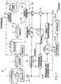
- Figure 1 illustrates the typical known in a schematic representation Construction of a Sagnac interferometer 30 in a closed loop arrangement.
- the light a light source 1 stabilized with respect to intensity, in particular a superluminescent diode (SLD) reaches a first one via a fiber link Beam splitter 2, also referred to as a coupler, from there via a polarizer 3 a second beam splitter, the main beam splitter 4.
- a fiber link Beam splitter 2 also referred to as a coupler
- polarizer 3 a second beam splitter
- the output signal of the detector 9 is first of all generated by an amplifier 10 raised and applied to a demodulator 16 on the one hand and a synchronous demodulator 19 on the other hand.
- the demodulator 16 forms together with one Gain filter 17 a scale factor controlled system.
- the synchronous demodulator 19 controls a ramp generator 21 via a filter 20, which is used for generation a reset signal is used.
- the resultant The output signal of the controllable amplifier 18 in turn is used for control of the first phase modulator 7, which corresponds to the optical phase modulates and resets.
- Sagnac interferometers of the type described above are usually used for measurement of rotation rates used. This is caused by rotation of the coil 6 Phase shift that the opposing partial beams due to Experienced Sagnac effect, determined, and on the rotation rate respectively the size of the rotation closed.
- suitable rotations now make possible rotations or interference effects switched off and instead a phase shift ⁇ , preferably via an additional, second phase modulator, by means of a measuring voltage U to a certain extent "artificially".
- the phase shift For example, ⁇ is compensated by a reset signal measured.
- the total throughput time T of the partial beams depends on Interferometer from one through a beam splitter, fiber links, phase modulators as well as a fiber coil defined part (coil part) of a light path of the Interferometer and thus of an optical length of the light path of this part from.
- the first part of the coil forms the actual measuring device Phase modulator 7 and the beam splitter 4 (second coupler) and the polarizer 3 typically combined in an IO chip.
- An optimal modulation frequency f of the interferometer in turn depends on the total throughput time T of the partial beams through the interferometer.
- the optical at regular time intervals Determines the length of the interferometer and the modulation frequency f thereafter regulated.
- the optical length can also be described in detail later Process for determining the voltage U introduced for correction become.
- ⁇ 2 ⁇ ⁇ .DELTA.T dn 2 dt l 2
- ⁇ is the wavelength of the light emitted by the light source 1.
- ⁇ T is the differential transit time of the partial beams through the part of the interferometer, which in this exemplary embodiment is defined by the beam splitter 4, the first phase modulator 7, the fiber path 26, and the fiber coil 6 minus the fiber path 27. ⁇ T thus corresponds to the time offset with which the partial beams pass through the second phase modulator 23.
- n 2 is the refractive index of the material 33 guiding the partial beams within the second phase modulator 23
- l 2 is the length of the electrodes 24 (FIG. 4).
- dn 2 / dU is generally a constant that essentially depends on the electro-optical behavior of the material 33 guiding the partial beams within the second phase modulator 23 and the distance between the modulator electrodes 24.
- dU / dt is the time derivative of the voltage U to be measured.
- c is the speed of light
- l 1 the length of the fiber material of the fiber sections 26 and 27, and that of the fiber coil 6 and the coupler 4 outside the phase modulators 23.
- n 1 denotes the refractive index of the fiber material.
- the product n 2 l 2 is to be understood as the optical length of the phase modulators 7, 23.
- optical lengths n 1 l 1 and n 2 l 2 are preferably measured here by a measurement module 31 integrated in the evaluation unit 40 of the interferometer.
- the time profile of the voltage U to be measured can alternatively be determined as follows:
- ⁇ 2 ⁇ f 1 is constant over time.
- the voltage curve U can thus be calculated from the time derivative dU / dt by multiplying the time derivative of U by the numerical value 1 / ⁇ and carrying out a phase shift of ⁇ / 2.
- f 1 must be known.
- the frequency f 1 can, however, be determined very precisely by determining the periodicity of dU / dt, that is to say by "tracking" dU / dt.
- This integration procedure has compared to the direct numerical integration procedure the advantage of a much higher accuracy.
- the method according to the invention has the advantage that the additional second phase modulator 23 an ideal separation of high voltage and measurement electronics can be realized.
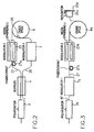
- the light obtained from the light source 1 via the coupler 2 is converted by a Polarizer 3a polarized and preferably at 45 ° against the polarization modes polarization-maintaining (PM) fiber (e.g. fiber pigtail) coupled in, so that two different partial beams are guided in the same fiber are mutually offset by 90 ° in polarization, i.e. effectively one use a different optical light path.
- PM polarization-maintaining
- the first sub-beam runs in one first polarization via a phase modulator 7a, that of the optical phase modulation for signal acquisition and possibly to reset the measured Phase shift ⁇ is used, a fiber supply 27a and a phase modulator 23a for the voltage U to be measured and a fiber coil 6a to form a ⁇ / 4 layer 25a with a reflector 25b (Fig. 3), which the reflected back light Rotates 90 ° in the polarization, and thus converted into a second polarization. Then the first partial beam runs the same again in the second polarization Way back to the polarizer 3a. Due to the second polarization, the returning first partial beam, however, not or at least only slightly modulated.
- modulators 7a, 23a both of which Conduct polarizations, but preferably only modulate one polarization.
- the second partial beam passes through the path to reflector 25b in the second polarization, and then changes back to the polarizer 3a in the first polarization. This modulates both beams at different times, which creates the phase shift ⁇ .
- the method described above has the advantage that the two partial beams run "simultaneously" in the same fiber, creating interference sources due to phase shift can be avoided in supply lines.
- FIGS. 1, 2, 4 and FIG. 5 a preferred embodiment of the device according to the invention explained.
- Integrated phase modulator 23 for example an integrated optical Chip (IO chip) is.
- the IO chip preferably consists of a lithium niobate (LiNbO3) crystal, in which, as shown in FIG. 4, one the opposite partial beams leading light guide path 33 is integrated. This runs partly between electrodes 24 also integrated in the IO chip, for example made of sputtered gold.
- a device 31 for determining the modulation frequency f is provided.
- the additional phase modulator 23 must be in the through the main beam splitter 4, the first phase modulator 7 and the fiber coil 6 defined part of the interferometer be integrated that the opposite beam generated on the main beam splitter 4 Partial rays go through this at different times, what through the differential cycle time ⁇ T is described.
- the device has 30 computing modules 28, 29 on.
- the computing module 28 calculates the time derivative of the one to be measured Voltage dU / dt according to formula (1) described above.
- the computing module 29 is for the temporal integration of those determined by the computing module 28 Function dU / dt according to one of the integration methods described above responsible.
- the fiber spool 6 is preferably designed such that it does not span an effective area, for example by a bifilar Winding of the fiber spool 6 is reached.
- a bifilar Winding of the fiber spool 6 is shown in FIG. 5: A reversal point 25 of the fiber spool 6 is placed so that the partial beams within the fiber spool 6 twice approximately the same geometric Pass through, with the two passes in opposite directions Directions are done. This is due to the Sagnac effect Phase shifts on.
- the computing modules 28, 29 can be either hardware-based or software-based be realized.
- the basic structure of the Sagnac interferometer described in FIG. 1 can in a further preferred embodiment approximately unchanged from Implementation of the method described above by means of FIG. 3 are used, by only the parts of the Interferometers from FIG. 1 are replaced with the corresponding parts from FIG. 3.
- the light path part 32 of the interferometer 30 has the 3, by means of the light in two partial beams different Polarization can be split.
- the polarization of light is determined by a polarization-maintaining fiber 27 with fiber supply 27a across the light path receive.
- the two modulators 7a and 23a are designed such that they modulate only light of a certain polarization.
- the fiber spool 6a is made also made of polarization-maintaining fiber.
- the reflector 25a, 25b corresponds the reversal point 25 of a bifilar wound coil according to FIG. 5.
- the fiber stocks 27a shown in FIGS. 2 and 3 are used for the purpose of the measuring voltage U applied phase modulators 23, 23a far from other components or the associated electronics.
- the inventive idea was applied to a fiber optic Sagnac interferometer described in closed loop structure.
- a realization is - for the Expertly visible - also possible in open-loop technology, if less Accuracy requirements allow such a cheaper solution in principle.
Abstract
Description
Die Erfindung betrifft ein Verfahren und eine Vorrichtung zur elektrooptischen Messung elektrischer Spannung.The invention relates to a method and a device for electro-optical Measurement of electrical voltage.
Es ist grundsätzlich bekannt, elektrische Ströme oder Spannungen über dadurch erzeugte eletromagnetische Felder mittels elektrooptischer Messmethoden zu messen (vergleiche beispielshalber DE 198 08 517 A1). Ein Beispiel für ein mögliches Einsatzgebiet der elektrooptischen Spannungsmessung stellt der Kraftwerkbereich dar, wo Messgeräte von der zu messenden Hochspannung ferngehalten werden sollen.It is basically known to pass electrical currents or voltages through it generated electromagnetic fields using electro-optical measurement methods to measure (see for example DE 198 08 517 A1). An example of a possible application of electro-optical voltage measurement is the Power plant area where measuring devices are kept away from the high voltage to be measured should be.
Bekannte optische Spannungsmessgeräte basieren beispielsweise auf dem physikalischen Prinzip eines Mach-Zehnder-Interferometers. In einem solchen Interferometer wird ein Lichtstrahl in mindestens zwei Teilstrahlen aufgespalten, die, nachdem sie definierte Wege zurückgelegt haben, wieder zu einem Strahl vereinigt werden. Die Intensität des wiedervereinigten Gesamtlichtstrahls ist aufgrund von Interferenz abhängig von einer möglichen Phasendifferenz der beiden Teilstrahlen. Diese Phasendifferenz wird bei optischen Spannungsmessgeräten durch die zu messende Spannung erzeugt, die den Lichtweg der Teilstrahlen beeinflussende Elektroden so beaufschlagt, dass die Teilstrahlen nach Durchlaufen der definierten Wege eine Phasendifferenz gegeneinander aufweisen, deren Betrag der Stärke der an den Elektroden anliegenden, zu messenden Spannung entspricht.Known optical voltage measuring devices are based, for example, on the physical Principle of a Mach-Zehnder interferometer. In such an interferometer a light beam is split into at least two partial beams, which, after covering defined paths, united again into a ray become. The intensity of the reunited overall light beam is due to of interference depending on a possible phase difference between the two Partial beams. This phase difference is used in optical voltage measuring devices generated by the voltage to be measured, which influences the light path of the partial beams Electrodes acted on so that the partial beams after passing through of the defined paths have a phase difference with respect to one another Amount of the strength of the voltage to be measured applied to the electrodes equivalent.
Um diese Phasendifferenz zu messen, wird üblicherweise über ein zweites Paar von Elektroden mit Hilfe eines Rückstellsignals eine zusätzliche Phasendifferenz erzeugt, die so geregelt wird, daß sie die durch die zu messende Spannung erzeugte Phasendifferenz gerade kompensiert. Damit ist die Größe der zusätzlichen Phasendifferenz ein Maß für die zu messende Spannung, und es kann aus der Größe des Rückstellsignals auf die zu messende Spannung geschlossen werden.To measure this phase difference, a second pair is usually used of electrodes with the aid of a reset signal an additional phase difference generated, which is controlled so that it is generated by the voltage to be measured Phase difference just compensated. So that's the size of the extra Phase difference is a measure of the voltage to be measured, and it can be derived from the Size of the reset signal can be concluded on the voltage to be measured.
Als nachteilig erweist sich hierbei, daß keine ideale Trennung von Hochspannung und Messelektronik möglich ist, da die Aufspaltung sowie die Zusammenführung der beiden Teilstrahlen vorzugsweise in einem einzigen integriert-optischen (IO)-Chip erfolgt, bei dem konstruktionsbedingt die jeweiligen Elektroden nahe beieinanderliegen. Die zu messende Hochspannung sowie das durch die Messelektronik erzeugte Rückstellsignal können sich somit gegenseitig stören.The disadvantage here is that there is no ideal separation of high voltage and measuring electronics is possible because the splitting as well as the merging of the two partial beams preferably in a single integrated optical (IO) -chip takes place where the respective electrodes depend on the design to be close together. The high voltage to be measured as well as that by the Reset signals generated by measuring electronics can thus interfere with each other.
Aus US 5,969,341 ist es beispielsweise bekannt, einen Spannungssensor zu verwenden, der eine räumliche Trennung von Messelektronik und Hochspannung ermöglicht. Es werden zwei Licht-Teilstrahlen verwendet, die auf unterschiedlichen, jeweils mittels Reflexion geschlossenen Wegen geführt werden. Die optischen Längen dieser Wege werden durch die zu messende Spannung verändert, wobei jedoch die Geometrie und die Brechungsindexdrift der beiden optischen Wege direkt die Messgenauigkeit beeinflussen und erheblich einschränken.From US 5,969,341 it is known, for example, to use a voltage sensor the spatial separation of measuring electronics and high voltage allows. Two partial light beams are used, which are on different, closed paths are led by reflection. The optical Lengths of these paths are changed by the voltage to be measured, however, the geometry and refractive index drift of the two optical Paths directly influence the measurement accuracy and significantly restrict it.
In DE 41 28 687 A1 ist ein Spannungssensor offenbart, bei dem zur Durchführung der Spannungsmessung ein Zwei-Moden-Laser und 2-Moden-Fasern, die durch einen Piezoring in ihrer optischen Länge beeinflußt werden, verwendet werden. Über die 2-Moden-Faser werden unterschiedliche optische Wege benutzt, deren Konstanz die Messgenauigkeit einschränken.DE 41 28 687 A1 discloses a voltage sensor in which to carry out the voltage measurement using a two-mode laser and 2-mode fibers are influenced by a piezo ring in their optical length used become. Different optical paths are used via the 2-mode fiber, whose constancy limits the measuring accuracy.
In DE 44 16 298 A1 ist ein diskretes, optisches Interferometer für Spannungsmessungen beschrieben, das einen elektrooptischen Kristall benutzt. Auch bei diesem Interferometer ist die Messgenauigkeit stark eingeschränkt, da der Mess- und der Referenzstrahl jeweils unterschiedliche optische Wege durchlaufen.DE 44 16 298 A1 describes a discrete, optical interferometer for voltage measurements that uses an electro-optical crystal. Also at The measuring accuracy of this interferometer is severely restricted, since the measuring and the reference beam each pass through different optical paths.
Der Erfindung liegt die Aufgabe zugrunde, ein Verfahren und eine Vorrichtung zur optischen Spannungsmessung bereitzustellen, mit denen sich eine hohe Messgenauigkeit erzielen lässt.The invention has for its object a method and an apparatus to provide for optical voltage measurement, with which a high Measurement accuracy can be achieved.
Die Erfindung ist bei einem Verfahren zur elektrooptischen Messung einer Spannung U erfindungsgemäß dadurch gekennzeichnet, dass in einem faseroptischen Sagnac-Interferometer zwei durch Teilung eines von einer Lichtquelle ausgehenden Lichtstrahls erzeugte Teilstrahlen zeitversetzt mittels eines Phasenmodulators moduliert werden, der durch die zu messende Spannung U beaufschlagt wird, wobei die bei Änderung der Spannung U entstehende Phasenverschiebung Ω beider Teilstrahlen gegeneinander gemessen, und basierend auf einer Spannungsnormaleichung der Phasenverschiebung Ω aus der gemessenen Phasenverschiebung Ω die an dem Phasenmodulator anliegende Spannung U errechnet wird.The invention relates to a method for the electro-optical measurement of a voltage U according to the invention characterized in that in a fiber optic Sagnac interferometer two by dividing one from a light source Partial beams generated by the light beam are shifted in time by means of a phase modulator be modulated, which is acted upon by the voltage U to be measured , the phase shift that occurs when the voltage U changes Ω of both partial beams measured against each other, and based on a voltage standard calibration the phase shift Ω from the measured phase shift Ω calculates the voltage U applied to the phase modulator becomes.
Eine Vorrichtung zur elektrooptischen Messung einer Spannung U ist erfindungsgemäß gekennzeichnet durch ein faseroptisches Sagnac-Interferometer, bei dem in einem Teil eines Lichtwegs, der Faserstrecken, eine Faserspule, einen ersten Phasenmodulator, einen Polarisator und einen Strahlteiler umfasst, ein zusätzlicher Phasenmodulator, der durch die zu messende Spannung U beaufschlagt wird, so integriert ist, dass an dem Strahlteiler erzeugte, gegenläufige Teilstrahlen bei Änderung der den zusätzlichen Phasenmodulator beaufschlagenden Spannung U eine Phasenverschiebung Ω gegeneinander erfahren, und durch eine Auswerteeinheit zur Bestimmung der an dem zusätzlichen Phasenmodulator anliegenden Spannung U aus der ermittelten Phasenverschiebung Ω.A device for the electro-optical measurement of a voltage U is according to the invention characterized by a fiber optic Sagnac interferometer, in which in a part of a light path, the fiber sections, a fiber coil, a comprises a first phase modulator, a polarizer and a beam splitter additional phase modulator, which is acted upon by the voltage U to be measured is integrated in such a way that opposing ones generated on the beam splitter Partial beams when the additional phase modulator is applied Voltage U experience a phase shift Ω against each other, and by an evaluation unit for determining the on the additional phase modulator applied voltage U from the determined phase shift Ω.
Vorteilhafte Weiterbildungen dieses Erfindungsgedankens sind in abhängigen
Patentansprüchen gekennzeichnet.
Die Erfindung und vorteilhafte Einzelheiten werden nachfolgend unter Bezug auf
die Zeichnung in beispielsweiser Ausführungsform näher erläutert. Es zeigen:
- Fig. 1
- das Prinzip-Blockschaltbild eines faseroptischen Sagnac-Interferometers in Closed-Loop-Aufbau mit digitaler Rückstellung, bei dem erfindungsgemäß ein durch die zu messende Spannung beaufschlagter Phasenmodulator in einen durch gegenläufige, von einem Strahlteiler ausgehende Teilstrahlen bestimmten Lichtweg integriert ist;
- Fig. 2
- eine Prinzipskizze eines über einen Strahlteiler in sich geschlossenen Lichtweges als ein Teil von Fig. 1, in den erfindungsgemäß ein durch die zu messende Spannung U beaufschlagter Phasenmodulator integriert ist, wobei der geschlossene Lichtweg von gegenläufigen Teilstrahlen durchlaufen wird, die von dem Strahlteiler ausgehen;
- Fig. 3
- eine Prinzipskizze eines durch Rückreflektion und 90°-Polarisationsdrehung mittels einer λ/4-Schicht in sich geschlossenen Weges, in den erfindungsgemäß ein durch die zu messende Spannung U beaufschlagter Phasenmodulator integriert ist, wobei der geschlossene Lichtweg durch gegenläufige Teilstrahlen durchlaufen wird, die vom Strahlteiler ausgehen;
- Fig. 4
- eine Prinzipskizze des von der zu messenden Spannung beaufschlagten Phasenmodulators zur Erläuterung des Funktionsprinzips der Erfindung; und
- Fig. 5
- eine schematische Darstellung einer drehratenunempfindlichen Spule mit bifilarer Wicklung.
The invention and advantageous details are explained in more detail below with reference to the drawing in an exemplary embodiment. Show it:
- Fig. 1
- the basic block diagram of a fiber optic Sagnac interferometer in a closed-loop design with digital reset, in which according to the invention a phase modulator acted upon by the voltage to be measured is integrated into a light path determined by opposing partial beams emanating from a beam splitter;
- Fig. 2
- a schematic diagram of a self-contained light path via a beam splitter as part of FIG. 1, in which, according to the invention, a phase modulator, which is acted upon by the voltage U to be measured, is integrated, the closed light path being traversed by opposing partial beams emanating from the beam splitter;
- Fig. 3
- a schematic diagram of a path closed in itself by back reflection and 90 ° polarization rotation by means of a λ / 4 layer, in which a phase modulator acted upon by the voltage U to be measured is integrated, the closed light path being traversed by opposing partial beams from the beam splitter go out;
- Fig. 4
- a schematic diagram of the phase modulator acted upon by the voltage to be measured to explain the operating principle of the invention; and
- Fig. 5
- a schematic representation of a rate-insensitive coil with bifilar winding.
Da Sagnac-Interferometer an sich bekannt sind, soll hier nur kurz unter Bezug auf die Zeichnungen auf deren prinzipielle Funktionsweise eingegangen werden.Since Sagnac interferometers are known per se, only a brief reference here the drawings on how they work in principle.
Figur 1 veranschaulicht in schematisher Darstellung den typischen bekannten Aufbau eines Sagnac-Interferometers 30 in Closed-Loop-Anordnung. Das Licht einer hinsichtlich Intensität stabilisierten Lichtquelle 1, insbesondere einer Superlumineszenzdiode (SLD) gelangt über eine Faserstrecke auf einen ersten Strahlteiler 2, auch als Koppler bezeichnet, von dort über einen Polarisator 3 auf einen zweiten Strahlteiler, den Hauptstrahlteiler 4. Von den beiden der Lichtquelle 1 abgewandten Aus-/Eingängen gelangen die durch Strahlteilung entstandenen Teilstrahlen auf die beiden Ein-/Ausgänge einer Faserspule 6, wobei zwischen den Aus-/Eingängen des Hauptstrahlteilers 4 bzw. den Ein-/Ausgängen der Faserspule 6 ein erster Phasenmodulator 7 angeordnet ist. Die im Hauptstrahlteiler 4 nach Durchlaufen der Faserspule 6 interferierenden Teilstrahlen durchlaufen wiederum den Polarisator 3 und werden über den ersten Strahlteiler 2 zu einem möglichst halben Anteil auf einen Fotodetektor 9 geleitet. Das Ausgangssignal des Detektors 9 wird zunächst durch einen Verstärker 10 angehoben und beaufschlagt einen Demodulator 16 einerseits und einen Synchrondemodulator 19 andererseits. Der Demodulator 16 bildet zusammen mit einem Verstärkungsfilter 17 eine Skalenfaktorregelstrecke. Der Synchrondemodulator 19 steuert über ein Filter 20 einen Rampengenerator 21 an, der zur Erzeugung eines Rückstellsignals dient. Das durch einen Modulationsoszillator 8 erzeugte Signal zum Verschieben des Arbeitspunktes in den Punkt höchster Empfindlichkeit und das Rückstellsignal werden durch einen Addierer 22 zu einem einzigen Signal zusammengesetzt und bilden das Eingangssignal eines regelbaren Verstärkers 18, welcher dieses Signal mit einem als Verstärkungsfaktor dienenden Ausgangssignal des Verstärkungsfilters 17 verstärkt. Das dadurch erhaltene Ausgangssignal des regelbaren Verstärkers 18 dient wiederum zur Ansteuerung des ersten Phasenmodulators 7, der die optische Phase entsprechend moduliert und rückstellt.Figure 1 illustrates the typical known in a schematic representation Construction of a Sagnac interferometer 30 in a closed loop arrangement. The light a light source 1 stabilized with respect to intensity, in particular a superluminescent diode (SLD) reaches a first one via a fiber link Beam splitter 2, also referred to as a coupler, from there via a polarizer 3 a second beam splitter, the main beam splitter 4. Of the two the light source 1 exit / entrances facing away reach those created by beam splitting Partial beams on the two inputs / outputs of a fiber spool 6, wherein between the outputs / inputs of the main beam splitter 4 or the inputs / outputs a first phase modulator 7 is arranged in the fiber coil 6. The in Main beam splitter 4 after passing through the fiber coil 6 interfering partial beams pass through the polarizer 3 again and are over the first Half of the beam splitter 2 is directed to a photodetector 9. The output signal of the detector 9 is first of all generated by an amplifier 10 raised and applied to a demodulator 16 on the one hand and a synchronous demodulator 19 on the other hand. The demodulator 16 forms together with one Gain filter 17 a scale factor controlled system. The synchronous demodulator 19 controls a ramp generator 21 via a filter 20, which is used for generation a reset signal is used. That generated by a modulation oscillator 8 Signal for shifting the working point to the point of highest sensitivity and the reset signal become one by an adder 22 single signal composed and form the input signal of a controllable Amplifier 18, which this signal with a serving as a gain factor Output signal of the gain filter 17 amplified. The resultant The output signal of the controllable amplifier 18 in turn is used for control of the first phase modulator 7, which corresponds to the optical phase modulates and resets.
Die erfindungsgemäßen, vom Stand der Technik abweichenden Teile des Interferometers sind mit der Bezugsziffer 32 bzw.40 gekennzeichnet.The parts of the interferometer according to the invention which differ from the prior art are identified by reference numbers 32 and 40, respectively.
Sagnac-Interferometer der oben beschriebenen Art werden in der Regel zur Messung von Drehraten eingesetzt. Dabei wird eine durch Drehung der Spule 6 verursachte Phasenverschiebung, die die gegenläufigen Teilstrahlen aufgrund des Sagnac-Effektes erfahren, ermittelt, und darüber auf die Drehrate beziehungsweise die Größe der Drehung geschlossen.Sagnac interferometers of the type described above are usually used for measurement of rotation rates used. This is caused by rotation of the coil 6 Phase shift that the opposing partial beams due to Experienced Sagnac effect, determined, and on the rotation rate respectively the size of the rotation closed.
Erfindungsgemäß werden nun durch geeignete Maßnahmen mögliche Drehungen bzw. Störeffekte ausgeschaltet und stattdessen eine Phasenverschiebung Ω, vorzugsweise über einen zusätzlichen, zweiten Phasenmodulator, mittels einer zu messenden Spannung U gewissermaßen "künstlich" erzeugt. Die Phasenverschiebung Ω wird beispielsweise durch deren Kompensation über ein Rückstellsignal gemessen.According to the invention, suitable rotations now make possible rotations or interference effects switched off and instead a phase shift Ω, preferably via an additional, second phase modulator, by means of a measuring voltage U to a certain extent "artificially". The phase shift For example, Ω is compensated by a reset signal measured.
Bekanntermaßen hängt die Gesamtdurchlaufzeit T der Teilstrahlen durch das Interferometer von einem durch einen Strahlteiler, Faserstrecken, Phasenmodulatoren sowie eine Faserspule definierten Teil (Spulenteil) eines Lichtweges des Interferometers und damit von einer optischer Länge des Lichtweges dieses Teils ab. Dabei sind im die eigentliche Messeinrichtung bildenden Spulenteil der erste Phasenmodulator 7 und der Strahlteiler 4 (zweiter Koppler) sowie der Polarisator 3 typischerweise in einem IO-Chip zusammengefasst. Eine optimale Modulationsfrequenz f des Interferometers hängt wiederum von der Gesamtdurchlaufzeit T der Teilstrahlen durch das Interferometer ab. Da die Faserstrecken zwecks unterschiedlicher Installationen variabel sein sollten und sich außerdem die optische Längen der Faserstrecken mit der Temperatur ändern, wird durch eine Auswerteeinheit des Interferomters in regelmäßigen zeitlichen Abständen die optische Länge des Interferometers bestimmt und die Modulationsfrequenz f danach geregelt. Die optische Länge kann außerdem in das später detailliert beschriebene Verfahren zur Ermittlung der Spannung U zur Korrektur eingebracht werden.As is known, the total throughput time T of the partial beams depends on Interferometer from one through a beam splitter, fiber links, phase modulators as well as a fiber coil defined part (coil part) of a light path of the Interferometer and thus of an optical length of the light path of this part from. The first part of the coil forms the actual measuring device Phase modulator 7 and the beam splitter 4 (second coupler) and the polarizer 3 typically combined in an IO chip. An optimal modulation frequency f of the interferometer in turn depends on the total throughput time T of the partial beams through the interferometer. Because the fiber strands are different Installations should be variable and also the optical Lengths of the fiber sections change with temperature by a Evaluation unit of the interferometer the optical at regular time intervals Determines the length of the interferometer and the modulation frequency f thereafter regulated. The optical length can also be described in detail later Process for determining the voltage U introduced for correction become.
Da es grundsätzlich bekannt ist, die optische Länge eines Interferometers zu messen, soll hier nur beispielhaft auf das Patent US 4,759,629 verwiesen werden, wo ein solches Verfahren sowie die Anpassung der Modulationsfrequenz f an die gemessene optische Länge beschrieben wird.Since it is generally known to increase the optical length of an interferometer measure, reference should only be made here by way of example to patent US 4,759,629, where such a method and the adjustment of the modulation frequency f to the measured optical length is described.
Im Folgenden wird der mathematische Zusammenhang zwischen der durch die zu messende Spannung U verursachte, am Detektor 9 beobachtbare Phasenverschiebung Ω und der zu messenden Spannung U anhand des in Figur 1 beziehungsweise 2 gezeigten Ausführungsbeispieles hergeleitet.In the following the mathematical connection between the through the Voltage U to be measured caused phase shift observable at detector 9 Ω and the voltage U to be measured using the one in FIG. 1 and 2 shown embodiment derived.
Allgemein gilt:
Aus Formel (1) folgt, dass aus der beobachteten Phasenverschiebung Ω auf die zeitliche Änderung der zu messenden Spannung dU/dt geschlossen werden kann, wenn die differentielle Durchlaufzeit ΔT bekannt ist. Diese ist nahezu konstant und läßt sich durch ein Spannungsnormal eichen. Diese wird vorzugsweise bei der Herstellung und/oder Installation des Spannungsmessgeräts durch Anlegen einer Normspannung an die Elektroden 24 des zweiten Phasenmodulators 23 und durch Erfassen der dadurch hervorgerufenen Phasenverschiebung Ω durchgeführt.From formula (1) it follows that from the observed phase shift Ω on the change over time of the voltage dU / dt to be measured can if the differential cycle time ΔT is known. This is almost constant and can be calibrated by a voltage standard. This is preferred in the manufacture and / or installation of the voltage measuring device by applying a standard voltage to the electrodes 24 of the second phase modulator 23 and by detecting the phase shift caused thereby Ω performed.
Um den Aufwand dieser Eichung gering zu halten, können die restliche Abhängigkeit
der differentiellen Durchlaufzeit ΔT von der Temperatur durch die Messung
der Gesamtdurchlaufzeit T und deren Temperaturabhängigkeit angenähert
werden. Es gilt für eine geregelte Modulationsfrequenz f:
Die Temperaturabhängigkeit von ΔT und damit von der berechneten Spannung U kann also aufgrund der Modulationsfrequenz f korrigiert werden, da T und ΔT durch gleiche Materialien beeinflusst werden.The temperature dependence of ΔT and thus of the calculated voltage U can therefore be corrected based on the modulation frequency f, since T and ΔT be influenced by the same materials.
Die Messung der optischen Längen n1l1 sowie n2l2 erfolgt hierbei vorzugsweise durch ein in die Auswerteeinheit 40 des Interferometers integriertes Messmodul 31.The optical lengths n 1 l 1 and n 2 l 2 are preferably measured here by a measurement module 31 integrated in the evaluation unit 40 of the interferometer.
Ist nach obigen Formeln die zeitliche Ableitung der zu messenden Spannung dU/dt über einen in der Auswerteeinheit 40 enthaltenen Rechenmodul 28 aus den gemessenen Größen ΔT sowie Ω bestimmt, so kann auf die Spannung U durch direkte Integration in der Zeit geschlossen werden. Diese Integrationsmethode hat den Vorteil, dass der zeitliche Verlauf der Spannung U auch bei zeitlich variablen Frequenzen der Spannung U wiedergebbar ist.According to the above formulas is the time derivative of the voltage to be measured dU / dt via a computing module 28 contained in the evaluation unit 40 the measured quantities ΔT and Ω are determined, the voltage U be closed by direct integration in time. This integration method has the advantage that the time profile of the voltage U also in the case of time variable frequencies of the voltage U is reproducible.
Liegt die zu messende Spannung U in Form einer Wechselspannung mit fester Frequenz f1 vor, so läßt sich der zeitliche Verlauf der zu messenden Spannung U auch alternativ wie folgt ermitteln:If the voltage U to be measured is in the form of an AC voltage with a fixed frequency f 1 , the time profile of the voltage U to be measured can alternatively be determined as follows:
Für die (Wechsel-)Spannung U gilt allgemein U = U0sin(ωt). Damit ergibt sich
deren zeitliche Ableitung dU/dt, welche aus der Messung der Phasenverschiebung
Ω sowie der Modulationsfrequenz f berechnet wird, zu dU/dt= U0ω cos(ωt).
Da der zeitliche Verlauf der Wechselspannung U durch Integration der zeitlichen
Ableitung dU/dt ermittelt wird, muss somit über eine cos- oder sin-Funktion integriert
werden. Für diese gilt:
Dies gilt unter der Voraussetzung, dass ω = 2πf1 zeitlich konstant ist. Damit lässt sich der Spannungsverlauf U aus der zeitlichen Ableitung dU/dt errechnen, indem die zeitliche Ableitung von U mit dem numerischen Wert 1/ω multipliziert und eine Phasenverschiebung von π/2 durchgeführt wird. Bei dieser Integrationsmethode muss f1 bekannt sein. Die Frequenz f1 läßt sich jedoch durch Ermittlung der Periodizität von dU/dt, also durch "Nachfahren" von dU/dt, sehr genau bestimmen.This applies provided that ω = 2πf 1 is constant over time. The voltage curve U can thus be calculated from the time derivative dU / dt by multiplying the time derivative of U by the numerical value 1 / ω and carrying out a phase shift of π / 2. With this integration method, f 1 must be known. The frequency f 1 can, however, be determined very precisely by determining the periodicity of dU / dt, that is to say by "tracking" dU / dt.
Dieses Integrationsverfahren hat gegenüber dem direkten numerischen Integrationsverfahren den Vorteil einer wesentlich höheren Genauigkeit. This integration procedure has compared to the direct numerical integration procedure the advantage of a much higher accuracy.
Wenn keine Wechselspannung vorliegt, wird gegebenenfalls ein Spannungs-Offset auf die durch die direkte Integration ermittelte Spannung addiert, da das Verfahren dann nicht zwingenderweise den absoluten Spannungswert U, sondern eventuell einen um eine Konstante verschobenen Spannungswert liefert.If there is no AC voltage, there may be a voltage offset added to the voltage determined by the direct integration, since the Then the process does not necessarily have the absolute voltage value U, but possibly provides a voltage value shifted by a constant.
Das erfindungsgemäße Verfahren hat den Vorteil, dass durch den zusätzlichen, zweiten Phasenmodulator 23 eine ideale Trennung von Hochspannung und Messelektronik realisiert werden kann.The method according to the invention has the advantage that the additional second phase modulator 23 an ideal separation of high voltage and measurement electronics can be realized.
Anhand von Figur 3 wird im Folgenden eine alternative Ausführungsform des erfindungsgemäßen Spannungsmeßverfahrens erläutert.3, an alternative embodiment of the invention is shown below Voltage measurement method explained.
Das von der Lichtquelle 1 über den Koppler 2 erhaltene Licht wird durch einen Polarisator 3a polarisiert und unter 45° gegen die Polarisationsmoden einer vorzugsweise polarisationserhaltenden (PM)-Faser (z. B. Faserpigtail) eingekoppelt, so dass in der gleichen Faser zwei verschiedene Teilstrahlen geführt werden, die gegeneinander um 90° in der Polarisation versetzt sind, also jeweils effektiv einen anderen optischen Lichtweg benutzen. Der erste Teilstrahl durchläuft in einer ersten Polarisation über einen Phasenmodulator 7a, der der optischen Phasenmodulation zur Signalgewinnung und u.U. zur Rückstellung der zu messenden Phasenverschiebung Ω dient, einen Faservorrat 27a und einen Phasenmodulator 23a für die zu messende Spannung U und eine Faserspule 6a zu einer λ/4-Schicht 25a mit einem Reflektor 25b (Fig. 3), der das zurückreflektierte Licht um 90° in der Polarisation dreht, und damit in eine zweite Polarisation überführt. Dann läuft der erste Teilstrahl in der zweiten Polarisation wieder den gleichen Weg zurück zu dem Polarisator 3a. Aufgrund der zweiten Polarisation wird der zurücklaufende erste Teilstrahl dabei aber nicht oder zumindest nur geringer moduliert. Dies wird durch Einsatz von Modulatoren 7a, 23a erreicht, die beide Polarisationen leiten, aber vorzugsweise nur eine Polarisation modulieren. Der zweite Teilstrahl durchläuft den Weg bis zum Reflektor 25b in der zweiten Polarisation, und wechselt dann beim Rücklaufen zum Polarisator 3a in die erste Polarisation. Dadurch werden beide Teilstrahlen zu unterschiedlichen Zeiten moduliert, wodurch die Phasenverschiebung Ω entsteht.The light obtained from the light source 1 via the coupler 2 is converted by a Polarizer 3a polarized and preferably at 45 ° against the polarization modes polarization-maintaining (PM) fiber (e.g. fiber pigtail) coupled in, so that two different partial beams are guided in the same fiber are mutually offset by 90 ° in polarization, i.e. effectively one use a different optical light path. The first sub-beam runs in one first polarization via a phase modulator 7a, that of the optical phase modulation for signal acquisition and possibly to reset the measured Phase shift Ω is used, a fiber supply 27a and a phase modulator 23a for the voltage U to be measured and a fiber coil 6a to form a λ / 4 layer 25a with a reflector 25b (Fig. 3), which the reflected back light Rotates 90 ° in the polarization, and thus converted into a second polarization. Then the first partial beam runs the same again in the second polarization Way back to the polarizer 3a. Due to the second polarization, the returning first partial beam, however, not or at least only slightly modulated. This is achieved by using modulators 7a, 23a, both of which Conduct polarizations, but preferably only modulate one polarization. The second partial beam passes through the path to reflector 25b in the second polarization, and then changes back to the polarizer 3a in the first polarization. This modulates both beams at different times, which creates the phase shift Ω.
Oben beschriebenes Verfahren hat den Vorteil, dass die beiden Teilstrahlen "gleichzeitig" in derselben Faser verlaufen, wodurch Störquellen durch Phasenverschiebung in Zuleitungen vermieden werden können. The method described above has the advantage that the two partial beams run "simultaneously" in the same fiber, creating interference sources due to phase shift can be avoided in supply lines.
Im Folgenden wird unter Bezugnahme auf die bereits erwähnten Figuren 1, 2, 4 und 5 eine bevorzugte Ausführungsform der erfindungsgemäßen Vorrichtung näher erläutert.In the following, reference is made to the already mentioned FIGS. 1, 2, 4 and FIG. 5 a preferred embodiment of the device according to the invention explained.
Im bereits beschriebenen, prinzipiellen Aufbau des Sagnac-Interferometers 30 sind durch die Erfindung im Wesentlichen die mit Bezugsziffer 32 bzw. 40 gekennzeichneten Teile betroffen, wobei die mit Bezugsziffer 32 gekennzeichneten Teile den geschlossenen, optischen Weg darstellen. In diesen ist, wie in Figur 1 gezeigt, vorzugsweise an einem Ende der Faserspule 6 in die Faserstrecken 26, 27 ein bereits erwähnter, zweiter, durch die zu messende Spannung U beaufschlagter Phasenmodulator 23 integriert, der beispielsweise ein integrierter optischer Chip (IO-Chip) ist. Der IO-Chip besteht vorzugsweise aus einem Lithiumniobat (LiNbO3)-Kristall, in den, wie in Fig. 4 gezeigt, eine die gegenläufigen Teilstrahlen führende Lichtleitstrecke 33 integriert ist. Diese verläuft teilweise zwischen ebenfalls in den IO-Chip integrierten Elektroden 24, die beispielsweise aus aufgesputtertem Gold bestehen. Weiterhin ist eine Einrichtung 31 zur Ermittlung der Modulationsfrequenz f vorgesehen.In the basic structure of the Sagnac interferometer 30 already described are essentially identified by the invention with reference numbers 32 and 40 respectively Parts affected, those marked with reference number 32 Show parts of the closed, optical path. In these, as in FIG. 1 shown, preferably at one end of the fiber spool 6 into the fiber sections 26, 27 a second, already mentioned, which is acted upon by the voltage U to be measured Integrated phase modulator 23, for example an integrated optical Chip (IO chip) is. The IO chip preferably consists of a lithium niobate (LiNbO3) crystal, in which, as shown in FIG. 4, one the opposite partial beams leading light guide path 33 is integrated. This runs partly between electrodes 24 also integrated in the IO chip, for example made of sputtered gold. There is also a device 31 for determining the modulation frequency f is provided.
Der zusätzliche Phasenmodulator 23 muß so in den durch den Hauptstrahlteiler 4, den ersten Phasenmodulator 7 sowie die Faserspule 6 definierten Teil des Interferometers integriert sein, daß die am Hauptstrahlteiler 4 erzeugten, gegenläufigen Teilstrahlen diesen zu unterschiedlichen Zeiten durchlaufen, was durch die differentielle Durchlaufzeit ΔT beschrieben wird.The additional phase modulator 23 must be in the through the main beam splitter 4, the first phase modulator 7 and the fiber coil 6 defined part of the interferometer be integrated that the opposite beam generated on the main beam splitter 4 Partial rays go through this at different times, what through the differential cycle time ΔT is described.
Zur Ermittlung der zu messenden Spannung U aus der Phasenverschiebung Ω sowie der differentiellen Durchlaufzeit ΔT weist die Vorrichtung 30 Rechenmodule 28, 29 auf. Der Rechenmodul 28 berechnet die zeitliche Ableitung der zu messenden Spannung dU/dt nach der oben beschriebenen Formel (1). Der Rechenmodul 29 ist für die zeitliche Integration der von dem Rechenmodul 28 ermittelten Funktion dU/dt nach einem der oben beschriebenen Integrationsverfahren zuständig.To determine the voltage U to be measured from the phase shift Ω and the differential throughput time ΔT, the device has 30 computing modules 28, 29 on. The computing module 28 calculates the time derivative of the one to be measured Voltage dU / dt according to formula (1) described above. The computing module 29 is for the temporal integration of those determined by the computing module 28 Function dU / dt according to one of the integration methods described above responsible.
Um den Einfluss eventueller, insbesondere aufgrund einer eventuellen Drehbewegung des Sagnac-Interferometers 30 verursachter unerwünschter Bewegungen möglichst gering zu halten, ist die Faserspule 6 vorzugsweise so gestaltet, dass sie keine effektive Fläche umspannt, was beispielsweise durch eine bifilare Wicklung der Faserspule 6 erreicht wird. Eine solche Wicklung ist in Fig. 5 gezeigt: Ein Umkehrpunkt 25 der Faserspule 6 ist hierbei so gelegt, dass die Teilstrahlen innerhalb der Faserspule 6 zweimal annähernd denselben geometrischen Weg durchlaufen, wobei die beiden Durchläufe in zueinander entgegengesetzten Richtungen erfolgen. Damit heben sich aufgrund des Sagnac-Effektes bewirkte Phasenverschiebungen auf.The influence of any, especially due to a possible rotary movement of the Sagnac interferometer 30 caused unwanted movements To keep it as low as possible, the fiber spool 6 is preferably designed such that it does not span an effective area, for example by a bifilar Winding of the fiber spool 6 is reached. Such a winding is shown in FIG. 5: A reversal point 25 of the fiber spool 6 is placed so that the partial beams within the fiber spool 6 twice approximately the same geometric Pass through, with the two passes in opposite directions Directions are done. This is due to the Sagnac effect Phase shifts on.
Die Rechenmodule 28, 29 können sowohl auf Hardware-Basis als auch auf Software-Basis realisiert sein.The computing modules 28, 29 can be either hardware-based or software-based be realized.
Der in Fig. 1 beschriebene prinzipielle Aufbau des Sagnac-Interferometers kann in einer weiteren bevorzugten Ausführungsform annähernd unverändert zur Durchführung des oben mittels Fig. 3 beschriebenen Verfahrens verwendet werden, indem lediglich die mit Bezugsziffer 32 bzw. 40 gekennzeichneten Teile des Interferometers aus Fig. 1 mit den entsprechenden Teilen aus Fig. 3 ersetzt werden.The basic structure of the Sagnac interferometer described in FIG. 1 can in a further preferred embodiment approximately unchanged from Implementation of the method described above by means of FIG. 3 are used, by only the parts of the Interferometers from FIG. 1 are replaced with the corresponding parts from FIG. 3.
Bei dieser Ausführungsform weist der Lichtwegteil 32 des Interferometers 30 den Polarisator 3a aus Fig. 3 auf, mittels dem Licht in zwei Teilstrahlen unterschiedlicher Polarisation aufspaltbar ist. Die Polarisierung des Lichts wird durch eine polarisationserhaltende Faser 27 mit Faservorrat 27a über den Lichtweg hinweg erhalten. Die beiden Modulatoren 7a und 23a sind derart beschaffen, dass sie nur Licht einer bestimmten Polarisation modulieren. Die Faserspule 6a besteht ebenfalls aus polarisationserhaltender Faser. Der Reflektor 25a, 25b entspricht dem Umkehrpunkt 25 einer bifilar gewickelten Spule nach Fig. 5.In this embodiment, the light path part 32 of the interferometer 30 has the 3, by means of the light in two partial beams different Polarization can be split. The polarization of light is determined by a polarization-maintaining fiber 27 with fiber supply 27a across the light path receive. The two modulators 7a and 23a are designed such that they modulate only light of a certain polarization. The fiber spool 6a is made also made of polarization-maintaining fiber. The reflector 25a, 25b corresponds the reversal point 25 of a bifilar wound coil according to FIG. 5.
Die in Figur 2 und 3 gezeigten Faservorräte 27a dienen dazu, die durch die zu messende Spannung U beaufschlagten Phasenmodulatoren 23, 23a fernab von anderen Bauteilen bzw. von der zugeordneten Elektronik zu installieren.The fiber stocks 27a shown in FIGS. 2 and 3 are used for the purpose of the measuring voltage U applied phase modulators 23, 23a far from other components or the associated electronics.
Der Erfindungsgedanke wurde in Anwendung auf ein faseroptisches Sagnac-Interferometer in Closed-Loop-Aufbau beschrieben. Eine Realisierung ist - für den Fachmann ersichtlich - auch in Open-Loop-Technik möglich, sofern geringere Genauigkeitsanforderungen eine solche prinzipiell kostengünstigere Lösung zulassen.The inventive idea was applied to a fiber optic Sagnac interferometer described in closed loop structure. A realization is - for the Expertly visible - also possible in open-loop technology, if less Accuracy requirements allow such a cheaper solution in principle.
Claims (22)
Applications Claiming Priority (2)
| Application Number | Priority Date | Filing Date | Title |
|---|---|---|---|
| DE2000144197 DE10044197B4 (en) | 2000-09-07 | 2000-09-07 | Method and device for electro-optical measurement of electrical voltage |
| DE10044197 | 2000-09-07 |
Publications (3)
| Publication Number | Publication Date |
|---|---|
| EP1186896A2 true EP1186896A2 (en) | 2002-03-13 |
| EP1186896A3 EP1186896A3 (en) | 2003-06-18 |
| EP1186896B1 EP1186896B1 (en) | 2006-01-18 |
Family
ID=7655368
Family Applications (1)
| Application Number | Title | Priority Date | Filing Date |
|---|---|---|---|
| EP20010119251 Expired - Lifetime EP1186896B1 (en) | 2000-09-07 | 2001-08-09 | Electro-optical method and apparatus for measuring an electrical voltage |
Country Status (2)
| Country | Link |
|---|---|
| EP (1) | EP1186896B1 (en) |
| DE (1) | DE10044197B4 (en) |
Cited By (2)
| Publication number | Priority date | Publication date | Assignee | Title |
|---|---|---|---|---|
| CN102128967A (en) * | 2010-12-15 | 2011-07-20 | 北京航空航天大学 | Optical fiber current transformer for three-phase common super-fluorescence optical fiber light source |
| CN106199125A (en) * | 2016-07-11 | 2016-12-07 | 国网北京经济技术研究院 | A kind of novel all-fiber current transformator and modulation-demo-demodulation method thereof |
Families Citing this family (3)
| Publication number | Priority date | Publication date | Assignee | Title |
|---|---|---|---|---|
| DE10339889B4 (en) * | 2003-08-29 | 2005-12-15 | Litef Gmbh | Method for determining / compensating for light source induced bias / random walk errors in Sagnac fiber optic interferometers |
| CN101621329B (en) * | 2008-07-03 | 2013-01-23 | 华为技术有限公司 | Method and system for measuring bias points of double-parallel modulator |
| CN111308157B (en) * | 2019-11-14 | 2022-06-17 | 许继集团有限公司 | All-fiber current transformer with quick set-up time and signal processing unit thereof |
Citations (5)
| Publication number | Priority date | Publication date | Assignee | Title |
|---|---|---|---|---|
| GB2243680A (en) * | 1990-05-02 | 1991-11-06 | Marconi Gec Ltd | Optical interferometer device |
| DE4128687A1 (en) * | 1991-08-29 | 1993-03-04 | Asea Brown Boveri | FIBER OPTICAL SENSOR |
| US5343036A (en) * | 1992-05-15 | 1994-08-30 | Asea Brown Boveri Ltd. | Optical measurement of electrical quantities using inverse piezoelectric effect with dual double-mode fiber |
| DE19808517A1 (en) * | 1998-02-27 | 1999-09-16 | Litef Gmbh | Current measurement device |
| WO2000019217A1 (en) * | 1998-09-30 | 2000-04-06 | Honeywell Inc. | In-line electro-optic voltage sensor |
Family Cites Families (5)
| Publication number | Priority date | Publication date | Assignee | Title |
|---|---|---|---|---|
| DE3528294A1 (en) * | 1984-08-09 | 1986-02-20 | Daimler-Benz Ag, 7000 Stuttgart | Method for the fibre-optical, spectrally coded transmission of the value of a variable physical measured quantity |
| FR2654827B1 (en) * | 1989-11-17 | 1992-03-20 | Photonetics | FIBER OPTIC MEASUREMENT DEVICE, GYROMETER, NAVIGATION AND STABILIZATION UNIT. |
| DE4416398A1 (en) * | 1994-05-10 | 1995-11-16 | Ebs Elektronische Bank Systeme | Vertical lifting door or gate |
| JPH10115644A (en) * | 1996-10-11 | 1998-05-06 | Toyota Central Res & Dev Lab Inc | Optical integrated voltage sensor |
| DE19842487C1 (en) * | 1998-09-16 | 2000-02-10 | Siemens Ag | Alternating magnetic field measuring method |
-
2000
- 2000-09-07 DE DE2000144197 patent/DE10044197B4/en not_active Expired - Fee Related
-
2001
- 2001-08-09 EP EP20010119251 patent/EP1186896B1/en not_active Expired - Lifetime
Patent Citations (5)
| Publication number | Priority date | Publication date | Assignee | Title |
|---|---|---|---|---|
| GB2243680A (en) * | 1990-05-02 | 1991-11-06 | Marconi Gec Ltd | Optical interferometer device |
| DE4128687A1 (en) * | 1991-08-29 | 1993-03-04 | Asea Brown Boveri | FIBER OPTICAL SENSOR |
| US5343036A (en) * | 1992-05-15 | 1994-08-30 | Asea Brown Boveri Ltd. | Optical measurement of electrical quantities using inverse piezoelectric effect with dual double-mode fiber |
| DE19808517A1 (en) * | 1998-02-27 | 1999-09-16 | Litef Gmbh | Current measurement device |
| WO2000019217A1 (en) * | 1998-09-30 | 2000-04-06 | Honeywell Inc. | In-line electro-optic voltage sensor |
Cited By (4)
| Publication number | Priority date | Publication date | Assignee | Title |
|---|---|---|---|---|
| CN102128967A (en) * | 2010-12-15 | 2011-07-20 | 北京航空航天大学 | Optical fiber current transformer for three-phase common super-fluorescence optical fiber light source |
| CN102128967B (en) * | 2010-12-15 | 2013-02-27 | 北京航空航天大学 | Optical fiber current transformer for three-phase common super-fluorescence optical fiber light source |
| CN106199125A (en) * | 2016-07-11 | 2016-12-07 | 国网北京经济技术研究院 | A kind of novel all-fiber current transformator and modulation-demo-demodulation method thereof |
| CN106199125B (en) * | 2016-07-11 | 2019-01-15 | 国网北京经济技术研究院 | A kind of novel all-fiber current transformator and its modulation-demo-demodulation method |
Also Published As
| Publication number | Publication date |
|---|---|
| EP1186896B1 (en) | 2006-01-18 |
| EP1186896A3 (en) | 2003-06-18 |
| DE10044197A1 (en) | 2002-04-04 |
| DE10044197B4 (en) | 2004-08-19 |
Similar Documents
| Publication | Publication Date | Title |
|---|---|---|
| DE3609507C2 (en) | Fiber optic interferometer | |
| DE3326555C2 (en) | ||
| DE69924531T2 (en) | KERREFFECT COMPENSATION FOR AN INTERFEROMETRIC FIBER OPTIC CIRCLE | |
| DE3144162A1 (en) | OPTICAL INTERFEROMETER DEVICE | |
| EP0652417B1 (en) | Fibre optic sagnac interferometer for rotation rate measurement with wavelength-stabilised light source | |
| EP0569700B1 (en) | Optical fiber sensor | |
| DE3136688A1 (en) | DEVICE FOR MEASURING ROTATIONAL SPEED | |
| DE2906870C2 (en) | ||
| EP0670469B1 (en) | Brillouin-ring laser gyro | |
| EP0538670A1 (en) | Passive ring resonator gyroscope | |
| DE3220389A1 (en) | METHOD AND DEVICE FOR MEASURING THE ROTATIONAL SPEED BY USING THE SAGNAC EFFECT | |
| EP0602075B1 (en) | Optical sensor for rotary movements | |
| DE2934794A1 (en) | Absolute rotation speed measurement - using monochromatic light ring with single sideband modulation of opposed partial light beams | |
| EP0436052B1 (en) | Fiber optic sagnac interferometer with digital phase resetting for measuring rotation rate | |
| DE10044197B4 (en) | Method and device for electro-optical measurement of electrical voltage | |
| DE60118662T2 (en) | Arrangement for measuring the electric current through the Faraday effect | |
| EP0529339B1 (en) | Fibre optic sensor | |
| DE102015106550B3 (en) | Fiber optic system and method for reducing bias errors in such a fiber optic system | |
| EP0864098B1 (en) | Process and device for measuring a quantity, in particular an electric current, with a high measurement resolution | |
| DE3039235A1 (en) | Pressure sensitive fibre=optic sensor e.g. hydrophone - has reacting fibre in series with optical delay line with light source coupled to one end of light path | |
| EP1597599B1 (en) | Optic fiber current sensor, comprising several sensing heads | |
| DE60105791T2 (en) | METHOD AND DEVICE FOR MEASURING THE PHASE DIFFERENCE BETWEEN INTENSITY MODULATED OPTICAL SIGNALS | |
| EP3401634A1 (en) | Distance measuring assembly for determining the distance to an object | |
| DE3001721A1 (en) | Measuring absolute rotation by sagnac effect - using light pulse modulation to reduce errors caused by light scattering | |
| CH686744A5 (en) | Fiberoptic current sensor. |
Legal Events
| Date | Code | Title | Description |
|---|---|---|---|
| PUAI | Public reference made under article 153(3) epc to a published international application that has entered the european phase |
Free format text: ORIGINAL CODE: 0009012 |
|
| AK | Designated contracting states |
Kind code of ref document: A2 Designated state(s): AT BE CH CY DE DK ES FI FR GB GR IE IT LI LU MC NL PT SE TR |
|
| AX | Request for extension of the european patent |
Free format text: AL;LT;LV;MK;RO;SI |
|
| PUAL | Search report despatched |
Free format text: ORIGINAL CODE: 0009013 |
|
| AK | Designated contracting states |
Designated state(s): AT BE CH CY DE DK ES FI FR GB GR IE IT LI LU MC NL PT SE TR |
|
| AX | Request for extension of the european patent |
Extension state: AL LT LV MK RO SI |
|
| 17P | Request for examination filed |
Effective date: 20031114 |
|
| AKX | Designation fees paid |
Designated state(s): CH DE FR GB IT LI |
|
| RBV | Designated contracting states (corrected) |
Designated state(s): CH FR GB IT LI SE |
|
| REG | Reference to a national code |
Ref country code: DE Ref legal event code: 8566 |
|
| 17Q | First examination report despatched |
Effective date: 20040513 |
|
| GRAP | Despatch of communication of intention to grant a patent |
Free format text: ORIGINAL CODE: EPIDOSNIGR1 |
|
| GRAS | Grant fee paid |
Free format text: ORIGINAL CODE: EPIDOSNIGR3 |
|
| GRAA | (expected) grant |
Free format text: ORIGINAL CODE: 0009210 |
|
| AK | Designated contracting states |
Kind code of ref document: B1 Designated state(s): CH FR GB IT LI SE |
|
| REG | Reference to a national code |
Ref country code: GB Ref legal event code: FG4D Free format text: NOT ENGLISH |
|
| REG | Reference to a national code |
Ref country code: CH Ref legal event code: EP |
|
| REG | Reference to a national code |
Ref country code: SE Ref legal event code: TRGR |
|
| REG | Reference to a national code |
Ref country code: CH Ref legal event code: NV Representative=s name: RENTSCH & PARTNER |
|
| GBT | Gb: translation of ep patent filed (gb section 77(6)(a)/1977) |
Effective date: 20060426 |
|
| ET | Fr: translation filed | ||
| PLBE | No opposition filed within time limit |
Free format text: ORIGINAL CODE: 0009261 |
|
| STAA | Information on the status of an ep patent application or granted ep patent |
Free format text: STATUS: NO OPPOSITION FILED WITHIN TIME LIMIT |
|
| 26N | No opposition filed |
Effective date: 20061019 |
|
| REG | Reference to a national code |
Ref country code: CH Ref legal event code: PCAR Free format text: RENTSCH & PARTNER;FRAUMUENSTERSTRASSE 9, POSTFACH 2441;8022 ZUERICH (CH) |
|
| PGFP | Annual fee paid to national office [announced via postgrant information from national office to epo] |
Ref country code: FR Payment date: 20090819 Year of fee payment: 9 |
|
| PGFP | Annual fee paid to national office [announced via postgrant information from national office to epo] |
Ref country code: CH Payment date: 20090824 Year of fee payment: 9 Ref country code: GB Payment date: 20090821 Year of fee payment: 9 Ref country code: SE Payment date: 20090821 Year of fee payment: 9 |
|
| PGFP | Annual fee paid to national office [announced via postgrant information from national office to epo] |
Ref country code: IT Payment date: 20090824 Year of fee payment: 9 |
|
| EUG | Se: european patent has lapsed | ||
| REG | Reference to a national code |
Ref country code: CH Ref legal event code: PL |
|
| GBPC | Gb: european patent ceased through non-payment of renewal fee |
Effective date: 20100809 |
|
| PG25 | Lapsed in a contracting state [announced via postgrant information from national office to epo] |
Ref country code: CH Free format text: LAPSE BECAUSE OF NON-PAYMENT OF DUE FEES Effective date: 20100831 Ref country code: LI Free format text: LAPSE BECAUSE OF NON-PAYMENT OF DUE FEES Effective date: 20100831 |
|
| REG | Reference to a national code |
Ref country code: FR Ref legal event code: ST Effective date: 20110502 |
|
| PG25 | Lapsed in a contracting state [announced via postgrant information from national office to epo] |
Ref country code: IT Free format text: LAPSE BECAUSE OF NON-PAYMENT OF DUE FEES Effective date: 20100809 |
|
| PG25 | Lapsed in a contracting state [announced via postgrant information from national office to epo] |
Ref country code: FR Free format text: LAPSE BECAUSE OF NON-PAYMENT OF DUE FEES Effective date: 20100831 |
|
| PG25 | Lapsed in a contracting state [announced via postgrant information from national office to epo] |
Ref country code: GB Free format text: LAPSE BECAUSE OF NON-PAYMENT OF DUE FEES Effective date: 20100809 |
|
| PG25 | Lapsed in a contracting state [announced via postgrant information from national office to epo] |
Ref country code: SE Free format text: LAPSE BECAUSE OF NON-PAYMENT OF DUE FEES Effective date: 20100810 |