EP1186895A1 - Improved RF test probe - Google Patents
Improved RF test probe Download PDFInfo
- Publication number
- EP1186895A1 EP1186895A1 EP01302470A EP01302470A EP1186895A1 EP 1186895 A1 EP1186895 A1 EP 1186895A1 EP 01302470 A EP01302470 A EP 01302470A EP 01302470 A EP01302470 A EP 01302470A EP 1186895 A1 EP1186895 A1 EP 1186895A1
- Authority
- EP
- European Patent Office
- Prior art keywords
- probe
- conductor
- termination
- insulator
- return
- Prior art date
- Legal status (The legal status is an assumption and is not a legal conclusion. Google has not performed a legal analysis and makes no representation as to the accuracy of the status listed.)
- Withdrawn
Links
- 239000000523 sample Substances 0.000 title claims abstract description 67
- 238000012360 testing method Methods 0.000 title abstract description 29
- 239000004020 conductor Substances 0.000 claims abstract description 60
- 239000012212 insulator Substances 0.000 claims abstract description 20
- 239000004065 semiconductor Substances 0.000 claims description 4
- 230000000694 effects Effects 0.000 abstract description 2
- 239000011810 insulating material Substances 0.000 abstract description 2
- 238000012544 monitoring process Methods 0.000 abstract 1
- 229920006362 Teflon® Polymers 0.000 description 2
- 239000011162 core material Substances 0.000 description 2
- 238000000034 method Methods 0.000 description 2
- 239000000463 material Substances 0.000 description 1
- 238000005259 measurement Methods 0.000 description 1
- 239000002184 metal Substances 0.000 description 1
- 238000001228 spectrum Methods 0.000 description 1
Images

Classifications
-
- G—PHYSICS
- G01—MEASURING; TESTING
- G01R—MEASURING ELECTRIC VARIABLES; MEASURING MAGNETIC VARIABLES
- G01R1/00—Details of instruments or arrangements of the types included in groups G01R5/00 - G01R13/00 and G01R31/00
- G01R1/02—General constructional details
- G01R1/06—Measuring leads; Measuring probes
- G01R1/067—Measuring probes
- G01R1/06772—High frequency probes
-
- G—PHYSICS
- G01—MEASURING; TESTING
- G01R—MEASURING ELECTRIC VARIABLES; MEASURING MAGNETIC VARIABLES
- G01R1/00—Details of instruments or arrangements of the types included in groups G01R5/00 - G01R13/00 and G01R31/00
- G01R1/02—General constructional details
- G01R1/06—Measuring leads; Measuring probes
- G01R1/067—Measuring probes
- G01R1/06711—Probe needles; Cantilever beams; "Bump" contacts; Replaceable probe pins
- G01R1/06733—Geometry aspects
- G01R1/06738—Geometry aspects related to tip portion
-
- G—PHYSICS
- G01—MEASURING; TESTING
- G01R—MEASURING ELECTRIC VARIABLES; MEASURING MAGNETIC VARIABLES
- G01R1/00—Details of instruments or arrangements of the types included in groups G01R5/00 - G01R13/00 and G01R31/00
- G01R1/02—General constructional details
- G01R1/06—Measuring leads; Measuring probes
- G01R1/067—Measuring probes
- G01R1/07—Non contact-making probes
Definitions
- the present invention relates to radio frequency circuits; more specifically, probes for testing radio frequency circuits.
- Radio frequency (RF) couplers were built into the circuit to provide test points to monitor the radio frequency signal in the circuit under test. This technique had the disadvantage of using precious circuit card real estate as well as adding the expense of RF couplers.
- Another technique for testing RF circuits involved using RF test probes with a bayonet type tip.
- One of the bayonet tips was used as a ground and the second bayonet tip was used to contact a radio frequency conductor such as a microstrip in the circuit under test.
- the bayonet tips often provided poor contact with either the microstrip or ground. Additionally, the bayonet probe affected the circuit under test and thereby distorted the RF signal to be measured.
- an RF test probe comprises a return conductor and a probing conductor.
- the probing conductor is positioned within an insulator, and a termination such as a 50 ohm resistor is electrically positioned between the ground conductor and probing conductor.
- the probe is used by placing a portion of the insulating material that surrounds the probe conductor in contact with a circuit such as an RF microstrip carrying an RF signal to be monitored.
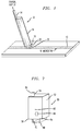
- FIG. 1 illustrates RF test probe 10 being used to measure an RF signal carried on RF microstrip 12.
- Coaxial output portion 14 of RF test probe 10 carries a signal representative of the RF signal on microstrip 12 to testing equipment such as an oscilloscope or spectrum analyzer.
- Handle 16 is used to provide a convenient non-conductive gripping surface for the user.
- Signal pickup section 18 includes insulator 20 and probe conductor 22. The probe is used by contacting an outer surface of insulator 20 to the conductor carrying the RF signal to be monitored.
- FIG. 2 is a side view of test probe 10.
- coaxial output portion 14 is shown with a threaded connector to facilitate connecting a cable used to provide a connection to testing equipment.
- coaxial conductor 28 continues until reaching handle end 30.
- the conductive shielding associated with the outer layer of coaxial conductor 28 is stripped away to expose a flexible insulator 20.
- insulator 20 It is possible to use the core material of the coaxial conductor as insulator 20; however, it is also possible to strip away the core material and use a flexible insulator such as a TEFLON® type material as insulator 20. (TEFLON® is a registered trademark of E. I.
- Probe conductor 22 which may be the center conductor of coaxial conductor 28, continues on a curved path through insulator 20 and reenters handle 16. Once reentering handle 16, probe conductor 22 is terminated in terminator 32. Terminator 32 is electrically positioned between probe conductor 22 and the return or ground conductor of coaxial conductor 28. The return conductor of coaxial conductor 28 may be external metal sheathing 34 or may be a conductive shield positioned below a non-conductive outer shield. Terminator 32 may be a resistor or semiconductive device such as a diode. If a resistor is used, it is preferable to use a resistance value that matches the characteristic impedance of the RF circuit under test. In many circuits, the characteristic impedance is typically 50 ohms and therefore terminator 32 is typically a 50 ohm resistor.
- FIG. 3 illustrates another side view of test probe 10.
- the view of FIG. 3 illustrates the view of FIG. 2 rotated 90 degrees.
- FIG. 4 is a cross section taken along line AA of FIG. 2.
- the cross section illustrates conductor 22 within insulator 20 and it also illustrates that insulator 20 has a circular cross section.
- arrow 40 illustrates the direction of the RF signal in the circuit under test relative to the probe to produce the maximum signal conducted through coaxial conductor 28. As a result, the probe may be rotated to determine the propagation direction of the RF signal being monitored.
- FIG. 5 is a cross section taken along line BB of FIG. 2.
- FIG. 5 once again illustrates that the cross section of insulator 20 is circular.
- the circular cross section offers the advantage of allowing the probe to be held at different angles when making contact with a conductor carrying an RF signal to be monitored.
- the circular cross section permits the probe to be held at different angles while maintaining the same distance between probe conductor 22 and the conductor carrying the signal to be monitored. This results in consistent measures of the signal to be monitored independent of the angle at which the probe is held.
- FIG. 6 illustrates an alternative cross section taken along line BB of FIG. 2.
- insulator 20 has at least a partial cross section that is substantially circular in a plane that is substantially perpendicular to probe conductor 22 that is passing through the cross section.
- This embodiment offers the advantage of providing a circular cross section along the areas where the probe would most likely contact the circuit under test while providing a flat cross section in areas where the probe is less likely to contact a circuit carrying a signal to be monitored.
- FIG. 7 illustrates an alternative embodiment to the invention.
- probe 50 includes handle 52 and coaxial conductor 54.
- Coaxial conductor 54 may include a threaded end at end section 56 to facilitate connection to a coaxial cable for connection to testing equipment.
- probe conductor 60 which may be the center conductor of coaxial conductor 54, emerges from the handle without outer conductive shield 62 of coaxial conductor 54. It should be noted that outer shield 62 may also act as a return or ground conductor.
- Probe conductor 60 extends out from handle 52 and then returns into handle 52 at position 64. After reentering handle 64, conductor 60 is terminated in terminator 66 which is electrically positioned between conductor 60 and return conductor 62.
- terminator 66 may be a resistor or semiconductor device such as a diode.
- Insulator 68 is positioned adjacent to the portion of probe conductor 60 that extends out of handle 52. The outer surface of insulator 68 is used to make contact to a conductor carrying an RF signal to be monitored. Insulator 68 may be attached directly to conductor 60 or it may be held in a spaced relationship to conductor 60 and attached to handle 52 for mechanical support.
- inventions may include configurations that permit an insulated surface adjacent to a probing conductor to be placed in contact with an RF circuit under test while a terminator is placed between the probe conductor and a return or ground conductor.
Landscapes
- Physics & Mathematics (AREA)
- General Physics & Mathematics (AREA)
- Measuring Leads Or Probes (AREA)
Abstract
Description
- The present invention relates to radio frequency circuits; more specifically, probes for testing radio frequency circuits.
- In the past, radio frequency circuits were tested usually using radio frequency (RF) couplers. Radio frequency couplers were built into the circuit to provide test points to monitor the radio frequency signal in the circuit under test. This technique had the disadvantage of using precious circuit card real estate as well as adding the expense of RF couplers.
- Another technique for testing RF circuits involved using RF test probes with a bayonet type tip. One of the bayonet tips was used as a ground and the second bayonet tip was used to contact a radio frequency conductor such as a microstrip in the circuit under test. The bayonet tips often provided poor contact with either the microstrip or ground. Additionally, the bayonet probe affected the circuit under test and thereby distorted the RF signal to be measured.
- The present invention provides an inexpensive RF test probe that provides a consistent measurement of an RF signal while having minimal effect on the circuit under test. In one embodiment of the present invention, an RF test probe comprises a return conductor and a probing conductor. The probing conductor is positioned within an insulator, and a termination such as a 50 ohm resistor is electrically positioned between the ground conductor and probing conductor. The probe is used by placing a portion of the insulating material that surrounds the probe conductor in contact with a circuit such as an RF microstrip carrying an RF signal to be monitored.
-
- FIG. 1 illustrates the RF test probe being used to measure an RF signal carried on an RF microstrip;
- FIG. 2 is a side view of the RF test probe;
- FIG. 3 is a second side view of the RF test probe;
- FIG. 4 is a cross section along line AA of FIG. 2;
- FIG. 5 is a cross section along line BB of FIG. 2;
- FIG. 6 illustrates an alternative cross section taken along line BB of FIG. 2; and
- FIG. 7 illustrates another embodiment of the RF test probe.
-
- FIG. 1 illustrates
RF test probe 10 being used to measure an RF signal carried onRF microstrip 12.Coaxial output portion 14 ofRF test probe 10 carries a signal representative of the RF signal onmicrostrip 12 to testing equipment such as an oscilloscope or spectrum analyzer.Handle 16 is used to provide a convenient non-conductive gripping surface for the user.Signal pickup section 18 includesinsulator 20 andprobe conductor 22. The probe is used by contacting an outer surface ofinsulator 20 to the conductor carrying the RF signal to be monitored. - FIG. 2 is a side view of
test probe 10. In this view,coaxial output portion 14 is shown with a threaded connector to facilitate connecting a cable used to provide a connection to testing equipment. Withinhandle 16,coaxial conductor 28 continues until reaching handle end 30. Athandle end 30, the conductive shielding associated with the outer layer ofcoaxial conductor 28 is stripped away to expose aflexible insulator 20. It is possible to use the core material of the coaxial conductor asinsulator 20; however, it is also possible to strip away the core material and use a flexible insulator such as a TEFLON® type material asinsulator 20. (TEFLON® is a registered trademark of E. I. duPont de Nemours and Company.)Probe conductor 22, which may be the center conductor ofcoaxial conductor 28, continues on a curved path throughinsulator 20 and reenters handle 16. Once reenteringhandle 16,probe conductor 22 is terminated interminator 32. Terminator 32 is electrically positioned betweenprobe conductor 22 and the return or ground conductor ofcoaxial conductor 28. The return conductor ofcoaxial conductor 28 may beexternal metal sheathing 34 or may be a conductive shield positioned below a non-conductive outer shield. Terminator 32 may be a resistor or semiconductive device such as a diode. If a resistor is used, it is preferable to use a resistance value that matches the characteristic impedance of the RF circuit under test. In many circuits, the characteristic impedance is typically 50 ohms and thereforeterminator 32 is typically a 50 ohm resistor. - FIG. 3 illustrates another side view of
test probe 10. The view of FIG. 3 illustrates the view of FIG. 2 rotated 90 degrees. - FIG. 4 is a cross section taken along line AA of FIG. 2. The cross section illustrates
conductor 22 withininsulator 20 and it also illustrates thatinsulator 20 has a circular cross section. Additionally,arrow 40 illustrates the direction of the RF signal in the circuit under test relative to the probe to produce the maximum signal conducted throughcoaxial conductor 28. As a result, the probe may be rotated to determine the propagation direction of the RF signal being monitored. - FIG. 5 is a cross section taken along line BB of FIG. 2. FIG. 5 once again illustrates that the cross section of
insulator 20 is circular. The circular cross section offers the advantage of allowing the probe to be held at different angles when making contact with a conductor carrying an RF signal to be monitored. The circular cross section permits the probe to be held at different angles while maintaining the same distance betweenprobe conductor 22 and the conductor carrying the signal to be monitored. This results in consistent measures of the signal to be monitored independent of the angle at which the probe is held. - FIG. 6 illustrates an alternative cross section taken along line BB of FIG. 2. In this case,
insulator 20 has at least a partial cross section that is substantially circular in a plane that is substantially perpendicular toprobe conductor 22 that is passing through the cross section. This embodiment offers the advantage of providing a circular cross section along the areas where the probe would most likely contact the circuit under test while providing a flat cross section in areas where the probe is less likely to contact a circuit carrying a signal to be monitored. - FIG. 7 illustrates an alternative embodiment to the invention. In this embodiment,
probe 50 includeshandle 52 andcoaxial conductor 54.Coaxial conductor 54 may include a threaded end atend section 56 to facilitate connection to a coaxial cable for connection to testing equipment. Atend 58 ofhandle 52probe conductor 60, which may be the center conductor ofcoaxial conductor 54, emerges from the handle without outerconductive shield 62 ofcoaxial conductor 54. It should be noted thatouter shield 62 may also act as a return or ground conductor.Probe conductor 60 extends out fromhandle 52 and then returns intohandle 52 atposition 64. After reenteringhandle 64,conductor 60 is terminated interminator 66 which is electrically positioned betweenconductor 60 and returnconductor 62. As mentioned earlier,terminator 66 may be a resistor or semiconductor device such as a diode.Insulator 68 is positioned adjacent to the portion ofprobe conductor 60 that extends out ofhandle 52. The outer surface ofinsulator 68 is used to make contact to a conductor carrying an RF signal to be monitored.Insulator 68 may be attached directly toconductor 60 or it may be held in a spaced relationship toconductor 60 and attached to handle 52 for mechanical support. - Other embodiments of the invention may include configurations that permit an insulated surface adjacent to a probing conductor to be placed in contact with an RF circuit under test while a terminator is placed between the probe conductor and a return or ground conductor.
Claims (19)
- An RF probe, characterized by:a conductive return;a insulating contact surface;a probe conductor positioned adjacent to the insulating contact surface; anda termination electrically positioned between the conductive return and the probe conductor.
- The RF probe of claim 1, characterized in that the conductive return is a ground return.
- The RF probe of claim 1, characterized in that the termination is a resistor.
- The RF probe of claim 3, characterized in that the termination is a resistor of approximately 50 ohms.
- The RF probe of claim 1, characterized in that the termination is a semiconductor device.
- The RF probe of claim 5, characterized in that the termination is a diode.
- An RF probe, characterized by:a conductive return;a probe conductor positioned within an insulator; anda termination electrically positioned between the conductive return and the probe conductor.
- The RF probe of claim 7, characterized in that the conductive return is a ground return.
- The RF probe of claim 7, characterized in that the termination is a resistor.
- The RF probe of claim 9, characterized in that the termination is a resistor of approximately 50 ohms.
- The RF probe of claim 7, characterized in that the termination is a semiconductor device.
- The RF probe of claim 11, characterized in that the termination is a diode.
- The RF probe of claim 7, characterized in that the insulator has at least a partial cross section that is substantially circular in a plane substantially perpendicular to the probe conductor.
- The RF probe of claim 13, characterized in that the conductive return is a ground return.
- The RF probe of claim 13, characterized in that the termination is a resistor.
- The RF probe of claim 15, characterized in that the termination is a resistor of approximately 50 ohms.
- The RF probe of claim 13, characterized in that the termination is a semiconductor device.
- The RF probe of claim 17, characterized in that the termination is a diode.
- An RF probe, characterized by:a conductive return;a probe conductor positioned within an insulator, the probe conductor being curved and the insulator having at least a partial cross section that is substantially circular in a plane substantially perpendicular to the probe conductor; anda termination electrically positioned between the conductive return and the probe conductor.
Applications Claiming Priority (2)
| Application Number | Priority Date | Filing Date | Title |
|---|---|---|---|
| US09/656,933 US6753676B1 (en) | 2000-09-07 | 2000-09-07 | RF test probe |
| US656933 | 2000-09-07 |
Publications (1)
| Publication Number | Publication Date |
|---|---|
| EP1186895A1 true EP1186895A1 (en) | 2002-03-13 |
Family
ID=24635179
Family Applications (1)
| Application Number | Title | Priority Date | Filing Date |
|---|---|---|---|
| EP01302470A Withdrawn EP1186895A1 (en) | 2000-09-07 | 2001-03-19 | Improved RF test probe |
Country Status (3)
| Country | Link |
|---|---|
| US (1) | US6753676B1 (en) |
| EP (1) | EP1186895A1 (en) |
| JP (1) | JP2002139514A (en) |
Cited By (1)
| Publication number | Priority date | Publication date | Assignee | Title |
|---|---|---|---|---|
| WO2012041578A1 (en) * | 2010-09-27 | 2012-04-05 | Ingun Prüfmittelbau Gmbh | High frequency test probe |
Families Citing this family (2)
| Publication number | Priority date | Publication date | Assignee | Title |
|---|---|---|---|---|
| US6956448B1 (en) * | 2002-12-17 | 2005-10-18 | Itt Manufacturing Enterprises, Inc. | Electromagnetic energy probe with integral impedance matching |
| US7053643B2 (en) * | 2004-03-25 | 2006-05-30 | Intel Corporation | Radio frequency (RF) test probe |
Citations (5)
| Publication number | Priority date | Publication date | Assignee | Title |
|---|---|---|---|---|
| JPS5590861A (en) * | 1978-12-28 | 1980-07-09 | Fujitsu Ltd | High-frequency coaxial probe |
| US5132607A (en) * | 1990-05-15 | 1992-07-21 | Shah Shirsh J | Electrical field strength sensing probe |
| EP0534826A1 (en) * | 1991-09-27 | 1993-03-31 | Thomson-Csf | Device for in situ ultra-high frequency broadband testing |
| EP0551564A2 (en) * | 1992-01-14 | 1993-07-21 | Hewlett-Packard Company | Non-contact test probe |
| US5834931A (en) * | 1996-10-31 | 1998-11-10 | Sematech, Inc. | RF current sensor |
Family Cites Families (7)
| Publication number | Priority date | Publication date | Assignee | Title |
|---|---|---|---|---|
| US3794914A (en) * | 1969-08-08 | 1974-02-26 | Narda Microwave Corp | Radiation detector employing resistive connected thermocouple elements |
| US3931573A (en) * | 1972-05-05 | 1976-01-06 | General Microwave Corporation | Radiation detector |
| US3919638A (en) * | 1973-08-10 | 1975-11-11 | Gen Electric | Microwave detection instrument |
| US4207518A (en) * | 1978-03-06 | 1980-06-10 | General Microwave Corporation | Broadband radiation detector with diode elements |
| US5748002A (en) * | 1996-01-26 | 1998-05-05 | Phase Dynamics Inc. | RF probe for montoring composition of substances |
| US5703928A (en) * | 1995-09-26 | 1997-12-30 | Industrial Technology, Inc. | Probe for sampling differential electromagnetic fields |
| US5952820A (en) * | 1996-02-16 | 1999-09-14 | Thrasher; M. D. | Foreign voltage detector |
-
2000
- 2000-09-07 US US09/656,933 patent/US6753676B1/en not_active Expired - Fee Related
-
2001
- 2001-03-19 EP EP01302470A patent/EP1186895A1/en not_active Withdrawn
- 2001-09-07 JP JP2001271372A patent/JP2002139514A/en active Pending
Patent Citations (5)
| Publication number | Priority date | Publication date | Assignee | Title |
|---|---|---|---|---|
| JPS5590861A (en) * | 1978-12-28 | 1980-07-09 | Fujitsu Ltd | High-frequency coaxial probe |
| US5132607A (en) * | 1990-05-15 | 1992-07-21 | Shah Shirsh J | Electrical field strength sensing probe |
| EP0534826A1 (en) * | 1991-09-27 | 1993-03-31 | Thomson-Csf | Device for in situ ultra-high frequency broadband testing |
| EP0551564A2 (en) * | 1992-01-14 | 1993-07-21 | Hewlett-Packard Company | Non-contact test probe |
| US5834931A (en) * | 1996-10-31 | 1998-11-10 | Sematech, Inc. | RF current sensor |
Non-Patent Citations (1)
| Title |
|---|
| PATENT ABSTRACTS OF JAPAN vol. 4, no. 142 7 October 1980 (1980-10-07) * |
Cited By (1)
| Publication number | Priority date | Publication date | Assignee | Title |
|---|---|---|---|---|
| WO2012041578A1 (en) * | 2010-09-27 | 2012-04-05 | Ingun Prüfmittelbau Gmbh | High frequency test probe |
Also Published As
| Publication number | Publication date |
|---|---|
| JP2002139514A (en) | 2002-05-17 |
| US6753676B1 (en) | 2004-06-22 |
Similar Documents
| Publication | Publication Date | Title |
|---|---|---|
| US6271673B1 (en) | Probe for measuring signals | |
| US4740746A (en) | Controlled impedance microcircuit probe | |
| US6724205B1 (en) | Probe for combined signals | |
| WO2004107401A3 (en) | Probe for testing a device under test | |
| JP2001099889A (en) | High frequency circuit inspection equipment | |
| US20070252606A1 (en) | Shielded Probe Apparatus for Probing Semiconductor Wafer | |
| EP1249706A3 (en) | Non-contact voltage measurement method and device, and related detection probe | |
| CA2695403A1 (en) | Measuring system for contactless decoupling of a signal running on a signal waveguide | |
| US6239587B1 (en) | Probe for monitoring radio frequency voltage and current | |
| US20100141241A1 (en) | Probe for measuring an electric field | |
| US20030115008A1 (en) | Test fixture with adjustable pitch for network measurement | |
| US6201400B1 (en) | Bulls-eye mid-frequency impedance probe | |
| GB2166913A (en) | Impedance matched test probe | |
| US6753676B1 (en) | RF test probe | |
| US20080186036A1 (en) | High Speed Electrical Probe | |
| US20070222468A1 (en) | High bandwidth probe system | |
| JPS623385B2 (en) | ||
| US6288555B1 (en) | Fixture for use in measuring an electrical characteristic of a pogo pin | |
| US6876183B2 (en) | Systems and methods for making a high-bandwidth coaxial cable connection | |
| JPH0541413Y2 (en) | ||
| US9279829B2 (en) | Apparatus and method for terminating probe apparatus of semiconductor wafer | |
| US5432457A (en) | Capacitive disk probe | |
| JPH07122602A (en) | High frequency probe and probe card | |
| JP2572932Y2 (en) | High frequency measurement probe | |
| JP2944677B2 (en) | Conductive contact |
Legal Events
| Date | Code | Title | Description |
|---|---|---|---|
| PUAI | Public reference made under article 153(3) epc to a published international application that has entered the european phase |
Free format text: ORIGINAL CODE: 0009012 |
|
| 17P | Request for examination filed |
Effective date: 20010329 |
|
| AK | Designated contracting states |
Kind code of ref document: A1 Designated state(s): AT BE CH CY DE DK ES FI FR GB GR IE IT LI LU MC NL PT SE TR Kind code of ref document: A1 Designated state(s): DE FR GB IT |
|
| AX | Request for extension of the european patent |
Free format text: AL;LT;LV;MK;RO;SI |
|
| 17Q | First examination report despatched |
Effective date: 20020625 |
|
| GRAH | Despatch of communication of intention to grant a patent |
Free format text: ORIGINAL CODE: EPIDOS IGRA |
|
| AKX | Designation fees paid |
Free format text: DE FR GB IT |
|
| RTI1 | Title (correction) |
Free format text: RF TEST PROBE |
|
| STAA | Information on the status of an ep patent application or granted ep patent |
Free format text: STATUS: THE APPLICATION HAS BEEN WITHDRAWN |
|
| 18W | Application withdrawn |
Effective date: 20030128 |