TECHNICAL FIELD
-
The present invention relates to an optical printer head,
in particular to an optical printer head including two or
more lines of light-emitting points. The present invention
further relates to a method of lighting up the optical
printer head.
BACKGROUND ART
-
A writing head of an optical printer, i.e. an optical
printer head is a light source for exposing a photosensitive
drum and comprises a line of light-emitting points consisting
of a light-emitting element array. The structure of an
optical printer including an optical printer head is shown in
Fig.1. An optically conductive material (photosensitive
material) such as amorphous Si is provided on the surface of
a cylindrical drum 2, which is rotated at the printing speed.
The surface of the photosensitive material is uniformly
charged with an electrostatic charger 4. Then, light
corresponding to a dot image being printed with an optical
print head 6 is projected onto the surface of the
photosensitive material to neutralize the charge on the area
to which the light is projected. Next, a developer 8
deposits the toner on the photosensitive material surface in
accordance with the charged pattern on the photosensitive
material surface. The transfer unit 10 transfers the toner
on a paper sheet 14 fed from a cassette 12. The toner on the
paper sheet is thermally fixed by the heat applied by a fixer
16, and the paper is sent to a stacker 18. Upon completion
of transfer, on the other hand, the charge on the drum is
neutralized over the entire surface with an erasing lamp 20,
and the remaining toner is removed by a cleaner 22.
-
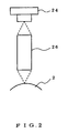
The construction of the optical print head 6 is shown in
Fig.2. This optical print head comprises a light-emitting
element array 24 and a rod-lens array 26, and the lens is
adapted so as to focus on the photosensitive drum 2.
-
In a conventional optical printer head, an array of
light-emitting points consists of one line of light-emitting
elements. The optical printer head including such one line
of light-emitting points has following problems.
- (1) The light exposure of one pixel is determined by the
amount of light of one light-emitting point lighted up.
Therefore, the light exposure of one pixel may not be
increased by the optical printer head consisting of one line
of light-emitting points.
- (2) In the optical printer head including one line of light-emitting
points, the density of pixels is determined by the
array pitch of light-emitting points. Also, the array pitch
of light-emitting points is limited by the manufacturing
condition of a light-emitting element array. Therefore,
there is a limitation for increasing the density of pixels in
the optical printer head including one line of light-emitting
points.
- (3) The light emitted from the light-emitting element array
is projected onto the lightsensitive drum through a rod-lens
array. At this time, if the rod-lens array has undulation in
the array direction thereof, a line of light spots formed
after passing through the rod-lens array may deviate from a
straight line.
- (4) While a light-emitting element array is fabricated by
arraying a plurality of light-emitting element array chips, a
line of light spots may deviate from a straight line due to
the inclined attachment of the chips.
-
DISCLOSURE OF THE INVENTION
-
An object of the present invention is to provide an
optical printer head in which light exposure of one pixel may
be increased.
-
Another object of the present invention is to provide an
optical printer head in which the density of pixels may be
increased.
-
A further object of the present invention is to provide
an optical printer head in which the deviation of a line of
light spots on a photosensitive drum may be corrected.
-
A still further object of the present invention is to
provide a method of lighting up in such an optical printer
head.
-
According to the first aspect of the present invention,
an optical printer head for exposing a photosensitive drum to
form pixels thereon is provided, which comprises a light-emitting
element array including two or more lines of light-emitting
points, and a rod-lens array for projecting light
emitted from the light-emitting array onto the photosensitive
drum to form a line of light spots.
-
It is preferable that each of the lines of light-emitting
points has the same pitch in a main-scanning
direction in parallel with an axis of rotation of the
photosensitive drum, and the light-emitting points of
respective lines of light-emitting points are arranged so as
to be lined up in a sub-scanning direction perpendicular to
the axis of rotation of the photosensitive drum, or the
light-emitting points of respective lines of light-emitting
points are arranged so as to be shifted in the main-scanning
direction.
-
Each of lines of light-emitting points may be composed
of an array of light-emitting diodes or an array of three-terminal
light-emitting thyristors. The array of three-terminal
light-emitting thyristors may be composed of a
light-emitting portion of a self-scanning light-emitting
element array.
-
The self-scanning light-emitting element array comprises
a transfer portion having such a construction that a
plurality of three-terminal light-emitting thyristor each
having such a construction that a plurality of transfer
elements each having a control electrode for controlling
threshold voltage or current for transfer operation are
arranged as transfer elements, said control electrodes of
said transfer elements are connected to the control electrode
of at least one transfer element located in the vicinity
thereof via an electrically unidirectional electrical element,
power-supply lines are connected to said transfer elements by
load resistors, and clock pulse lines are connected to the
transfer element ; and a light-emitting portion having such a
construction that a plurality of three-terminal light-emitting
thyristor each having a control electrode for
controlling threshold voltage or current are arranged as
light-emitting elements, the control electrodes of said
light-emitting element are connected to the control
electrodes of the transfer elements by electrical means, and
lines for applying current for light emission to the light-emitting
element are provided.
-
According to the second aspect of the present invention,
in an optical printer head comprising a light-emitting
element array including two or more lines of light-emitting
points, and a rod-lens array for projecting light emitted
from the light-emitting array onto the photosensitive drum to
form a line of light spots, wherein each of the lines of
light-emitting points has the same pitch in a main-scanning
direction in parallel with an axis of rotation of the
photosensitive drum, and the light-emitting points of
respective lines of light-emitting points are arranged so as
to be lined up in a sub-scanning direction perpendicular to
the axis of rotation of the photosensitive drum, a method of
lighting up the light-emitting points comprises a step of
selecting the lighting up of a plurality of light-emitting
points lined up in the sub-scanning direction to vary the
accumulated amount of light of the pixels. In this case, the
amounts of light of the light-emitting points in the two or
more lines of light-emitting points are all the same, or are
varied every a line of light-emitting points.
-
It is also preferable to select the lighting up the
light-emitting points in the two or more lines of light-emitting
points to correct the deviation of the line of light
spots on the photosensitive drum.
BRIEF DESCRIPTION OF THE DRAWINGS
-
- Fig.1 is a schematic diagram of an optical printer
comprising an optical printer head.
- Fig.2 is a schematic diagram of the structure of an
optical printer head.
- Fig.3 is a schematic diagram of a light-emitting diode
array chip comprising two lines of light-emitting points.
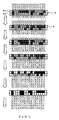
- Fig.4 is a schematic diagram showing the situation where
the photosensitive drum is exposed during the drum is rotated.
- Fig.5 is a schematic diagram showing another situation
where the photosensitive drum is exposed during the drum is
rotated.
- Fig.6 is a schematic diagram of an another example of
light-emitting diode array chip used in an optical printer
head.
- Fig.7 is a schematic diagram showing the situation where
a line of light spots deviate from a straight line due to the
influence by undulation of the rod-lens array.
- Fig.8 is a schematic diagram showing an example of
correction for the deviation of a line of light spots shown
in Fig.7.
- Fig.9 is an equivalent circuit diagram of a self-scanning
light-emitting element array.
- Fig.10 is a schematic diagram of the self-scanning
light-emitting element array chip shown in Fig.9.
-
BEST MODE FOR CARRYING OUT THE INVENTION
-
The embodiments of the present invention will now be
described with reference to the drawings.
Embodiment 1
-
Referring to Fig.3, there is shown a light-emitting
diode (LED) array chip 30 comprising two lines, i.e. a first
and second lines of light-emitting point. In the figure,
reference numeral 32 designates a bonding pad and 34 a light-emitting
point. "p" denotes the array pitch of light-emitting
points in a main-scanning direction, and "d" the
pitch of light-emitting points in a sub-scanning direction.
Herein, the main-scanning direction is a direction in
parallel with an axis of rotation of the photosensitive drum,
and the sub-scanning direction is a direction perpendicular
to the axis of rotation of the drum. It should be noted that
"d" is selected so as to be integral multiples of resolution
in a sub-scanning direction.
-
An example of exposure with a printer head 6 comprising
two lines of light-emitting points is illustrated with
reference to Fig.4. In the figure, 6A and 6B designate a
first and second lines of light-emitting points, respectively.
It is assumed that the amounts of light of respective light-emitting
points of the first and second lines are the same.
Fig.4 shows the situation where the photosensitive drum is
exposed with the two lines of light-emitting points during
the rotation of the drum in a sub-scanning direction. In the
figure, one block 9 designates one pixel, and a darken block
in the optical printer head denotes a light-emitting point
lighted up. Numeral "0" denotes a pixel which was no exposed,
"1" a pixel which was exposed one time, and "2" a pixel which
was exposed two times, respectively. As apparent from the
figure, one time exposure is carried out by the first line of
the light-emitting points 6A, and two time exposures are
carried out at first by the first line of the light-emitting
points 6A and then by the second line of the light-emitting
points 6B. It is appreciated that the exposure state of
three steps for a pixel, i.e. "0", "1" and "2" may be formed
by use of the head comprising two lines of light-emitting
points.
-
According to the optical printer head of this embodiment,
the printing speed may be increased by two times compared
with the conventional optical printer head comprising one
line of light-emitting points, because the accumulated light
exposure on a pixel becomes at maximum two time that of the
conventional one.
-
While the optical printer head comprising two lines of
light-emitting points is illustrated in the embodiment
described above, three or more lines of light-emitting points
may be used.
-
Another example of exposure with a printer head
comprising two lines of light-emitting points is illustrated
with reference to Fig.5. While the amounts of light of
respective light-emitting points of the first and second
lines are the same in the former example, the amount of light
of the second line of light-emitting points is two times that
of the first line of light-emitting points in this embodiment.
-
With the amounts of light of the first and second lines
of light-emitting points being different in this manner, the
exposure state of four steps, i.e. "0", "1", "2" and "3" may
be implemented. However, the amount of light of the first
line of light-emitting points is set to the half of that the
second line of light-emitting points, so that the accumulated
light exposure is at most 1.5 times compared with the example
of Fig.4. As a result, the example illustrated in Fig.4 is
superior to this example in respect of printing speed of the
printer.
-
While the optical printer head comprising two lines of
light-emitting points is illustrated in this embodiment,
three or more lines of light-emitting points may be used.
Embodiment 2
-
Referring to Fig.6, there is shown an LED array chip 36
which is used as an another example in an optical printer
head. In the figure, reference numeral 32 designates a
bonding pad, and 34 a light-emitting point.
-
In this embodiment, an optical printer head is
structured by utilizing the LED array chip 36 comprising a
first and second lines of light-emitting points arranged with
the pitch "p" in a main-scanning direction and the pitch "d"
in a sub-scanning direction. The first and second lines of
light-emitting points are shifted by half pitch (p/2) to each
other in a main-scanning direction as shown in the figure.
It should be noted that the sub-scanning direction pitch "d"
is selected so as to be integral multiples of resolution in a
sub-scanning direction.
-
using the LED array chip having above-described
structure, it may be possible to fabricate an optical printer
head having pixel density in a main-scanning direction which
is two times compared with the head in Fig.3.
Embodiment 3
-
As shown in Fig.2, the light emitted from the light-emitting
element array 24 impinges upon the photosensitive
drum 2 through the rod-lens array 26. The rod-lens array 26
is structured by stacking rod-lenses alternately as shown in
Fig.7.
-
The light 52 emitted from a line of light-emitting
points 40 consisting of an array of LEDs 39 passes through
the rod-lens array 26. The light 52 passed through the rod-lens
array impinges upon the photosensitive drum 2 to form a
line of light spots 42 each light spot being designated by
reference numeral 41.
-
The line of light spots 42 may deviate from a straight
line due to the influence by undulation of the rod-lens array
26. In order to correct the deviation of a line of light
spots 42, an LED array as a light source is constructed by a
plurality of lines of light-emitting points.
-
Fig.8 shows an embodiment comprising an LED array 44
consisting of four lines of light-emitting points 44-1, 44-2,
44-3 and 44-4. According to the present embodiment, two
light-emitting points neighbored in a sub-scanning direction
are lighted up at the same time to enable three steps of
alignment for light spots. The hatching areas in the LED
array 44 show the adjacent two light-emitting points lighted
up at the same time, respectively. The hatching areas in a
line of light spots 46 show the light impinged upon the
photosensitive drum 2 passing through the rod-lens array 26,
respectively.
-
As shown in Fig.8, a line of light spots which are
arranged in a substantially straight line manner may be
implemented by selecting the light-emitting points to be
lighted up in the LED array 44 to correct the influence due
to the modulation of the rod-lens array 26.
-
It is also possible to correct the deviation of a line
of light spots due to the inclined attachment of the chips.
Embodiment 4
-
While an LED array is used as an light-emitting element
in the three embodiment described above, the case where a
self-scanning light-emitting element array using three-terminal
light-emitting thyristors is used for an optical
printer head will be explained in this embodiment.
-
Referring to Fig.9, there is shown an equivalent circuit
of a self-scanning light-emitting element array. This self-scanning
light-emitting element array has been disclosed in
Japanese Patent Publication No.2-263668 which is hereby
incorporated by reference.
-
The self-scanning light-emitting element array in Fig.9
generally comprises a transfer portion 60, a first light-emitting
portion 62, and a second light-emitting portion 64.
The first light-emitting portion 62 corresponds to the first
line of light-emitting points and the second light-emitting
portion 64 corresponds to the second line of light-emitting
points in the described-above embodiments.
-
The transfer portion 60 uses three-terminal light-emitting
thyristor ..., T-1, T0, T1, .... A power supply voltage
VGA (-5V) is applied to each gate electrode ... G-1, G0, G1, ...
of the thyristors through each load resistor RL. Neighboring
gate electrodes are electrically connected via each diode ...
D-1, D0, D1, .... to obtain electrical interaction. Each of two
transfer clock lines (1 and 2) is connected to the anode
electrode of each light-emitting thyristor on every other
element. s designates a start pulse in the figure.
-
The first and second light-emitting portions 62 and 64
comprise arrays of the three-terminal light-emitting
thyristors (.., L1-1, L10, L11, ...), (..., L2-1, L20, L21, ...) as
writing light-emitting elements. Respective gate electrodes
of the light-emitting thyristors of the light-emitting
portions 62 and 64 are correspondingly connected to the gate
electrodes of the light-emitting thyristors of the transfer
portion 60. Write signals I1 and I2 are connected to the
cathodes electrodes of the light-emitting thyristors (..., L1-1,
L10, L11, ...) and (..., L2-1, L20, L21, ...), respectively.
-
The operation of the transfer portion 60 will now be
described. Assume that when the transfer clock 1 is driven
to a low level, the light-emitting thyristor T0 is turned on.
At this time, the voltage of the gate electrode G0 is
increased to a level near zero volts due to the
characteristic of the three-terminal light-emitting thyristor.
The gate voltage of each light-emitting thyristor is
determined by the network of the resistors RL and diodes ...,
D-1, D0, D1, .... The gate voltage of a thyristor nearest to
the light-emitting thyristor T0 increases most, and the gate
voltages of other thyristors decrease as they are further
away from the thyristor T0.
-
The voltage reducing effect works only in the rightward
direction from the thyristor T0 due to the unidirectionality
and asymmetry of diode characteristics. That is, the gate
electrode G1 is set at a lower voltage with respect to G0 by
a forward rise voltage Vdif of the diode, while the gate
electrode G2 is set at a lower voltage with respect to G1 by
a forward rise voltage Vdif of the diode. On the other hand,
current does not flow in the gate electrode G-1 on the left
side of the thyristor T0 because the diode D-1 is reverse-biased.
As a result, the gate electrode G-1 is at the same
potential as the power supply voltage VGA.
-
Although the next transfer clock pulse 2 is applied to
the nearest light-emitting thyristors T1, T-1, and T3 and T-3,
the thyristor having the highest turn-on voltage among them
is T1, whose turn-on voltage is approximately the gate
voltage of G1 + Vdif, about twice as high as Vdif. The
thyristor having the second highest turn-on voltage is T3,
about four times as high as Vdif. The turn-on voltage of T-1
and T-3 is about VGK + Vdif.
-
It follows from the above discussion that by setting the
low-level voltage of the transfer clock pulse to a level
about twice to four times as high as Vdif, only the light-emitting
thyristor T1 is turned on to perform a transfer
operation.
-
Next, the operation of the first light-emitting portion
62 be described. Assuming that the transfer element T0 is in
on-state, the voltage of the gate electrode G0 is increased
more than the power supply voltage VGA (-5 volts) and is
driven to about 0 volts. Therefore, if the voltage of the
write signal I1 is lower than the diffusion voltage (about
1 volt) of PN junction, the light-emitting thyristor L10 may
be turned into an on-state (i.e., a light-emitting state).
-
On the other hand, the voltage of the gate electrode G-1
is about -5 volts, and the voltage of the gate electrode G1
is about -1 volt. Consequently, the write voltage of the
light-emitting thyristor L1-1 is about -6 volts, and the
write voltage of the light-emitting thyristor L11 is about -2
volts. It is recognized from this that the voltage of the
write signal I1 which can write into only the light-emitting
thyristor L10 is in a range of about -1 to -2 volts.
When the light-emitting thyristor L10 is turned on, i.e., in
the light-emitting state, there is no possibility that
another light-emitting thyristor is selected and turned on.
-
The amount of light emitted from the thyristor is
determined by a current due to the write signal I1.
Accordingly, the light-emitting elements may emit light at
any desired amount of light. In order to transfer on-state
to the next thyristor, it is necessary to turn off the
thyristor in on-state by temporarily dropping the voltage of
the write signal I1 down to zero volts.
-
The operation of the light-emitting portion 64 is the
same as that of the first light-emitting portion 62.
Therefore, the explanation thereof will be omitted.
-
Referring to Fig.10, there is shown the self-scanning
light-emitting element array chip 110 illustrated in Fig.9.
Reference numeral 70 designates a bonding pad in the figure.
In the chip 110, the transfer portion 60, the two lines of
light-emitting points 62, 64, and a plurality of bonding pads
70 are formed. Such self-scanning light-emitting element
array may be used in the optical printer head in the same
manner as the LED array shown in Fig.3. In a conventional
LED array, the light-emitting points and the bonding pads are
connected one to one, so that when the number of lines of
light-emitting points are plural, the number of bonding pads
also becomes multiple of said number of lines. On the
contrary, the number of bonding pads increases by one as the
number of the lines of light-emitting points increases by one
in the self-scanning light-emitting element array, resulting
in the advantage such that the size of a chip is not
increased.
INDUSTRIAL APPLICABILITY
-
According to the present invention, as described above,
two or more lines of light spots are provided in an optical
printer head. As a result, following advantages may be
obtained, i.e., (1) the light exposure may be increased, (2)
the pixel density may be increased, (3) the deviation of a
line of light spots due to the undulation of a rod-lens array
and the inclined attachment of the chip, and (4) the printing
speed of the printer may be increased.